
I have followed the rise of the perovskite solar cell with great interest because it combines low-cost materials with exceptional optoelectronic properties. In my assessment, the perovskite solar cell is now moving from laboratory curiosity to pre-commercial technology, but the manufacturing route remains unsettled. Solution processing has produced record power conversion efficiencies, yet it struggles with uniformity over large areas, solvent-induced defects, and compatibility with textured silicon bottom cells. Chemical vapor deposition offers a solvent-free alternative that is already well established in thin-film industries. I therefore focus this article on how chemical vapor deposition can be used to fabricate the perovskite solar cell and what must still be solved before gigawatt-scale production becomes feasible.
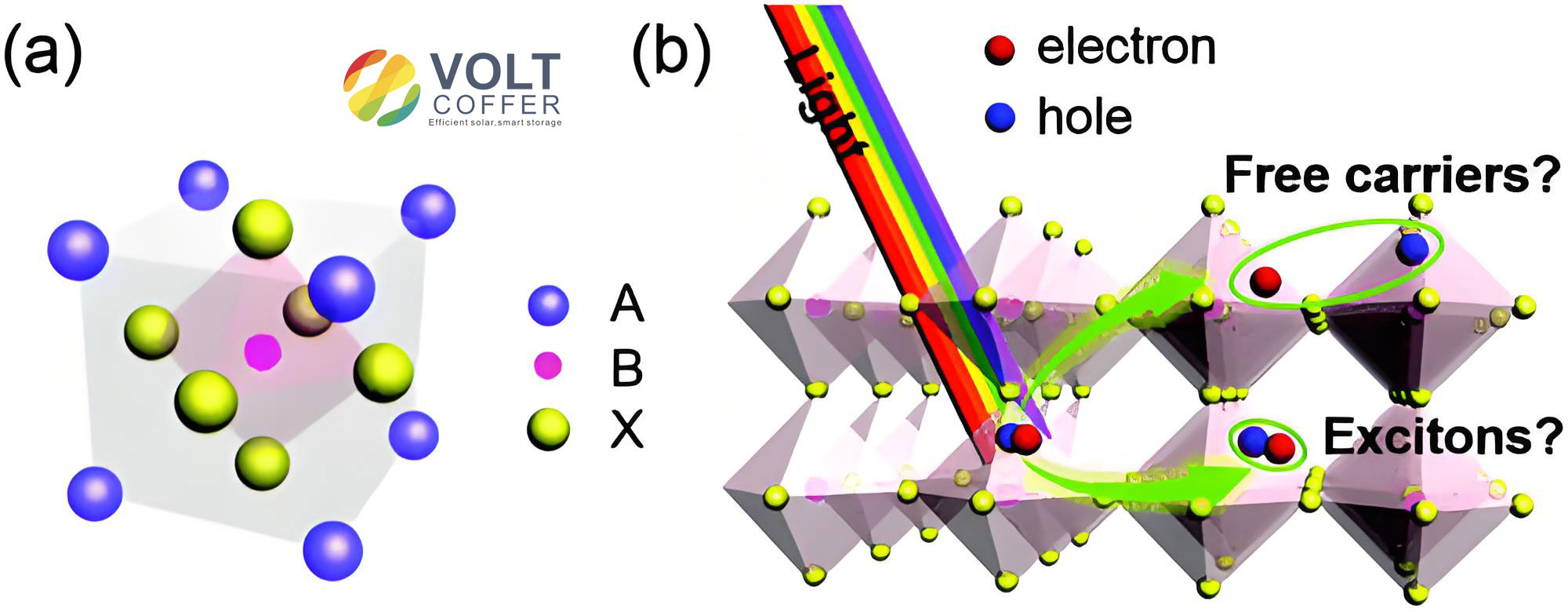
I begin with the core motivation. A perovskite solar cell typically uses an organic–inorganic halide perovskite as the light absorber, for example methylammonium lead iodide, formamidinium lead iodide, or mixed-cation mixed-halide compositions. The absorber must be uniform, phase-pure, and free of pinholes to achieve high efficiency and long-term stability. In a vapor-solid reaction, an inorganic precursor film such as lead iodide or cesium bromide reacts with an organic vapor such as methylammonium iodide or formamidinium iodide. The reaction is fast, but the diffusion of organic species into the inorganic framework is slow, so the overall rate is often diffusion-limited. This balance between reaction and diffusion is the key to controlling film quality in a perovskite solar cell made by chemical vapor deposition.
I also note that chemical vapor deposition is not a single technique. It includes tube furnaces, multi-zone reactors, showerhead systems, and close-spaced sublimation. Each configuration changes the temperature field, the gas flow, and the distance between the precursor source and the substrate. Because the perovskite solar cell requires precise stoichiometry, these engineering details directly determine phase purity and device performance. In the following sections I describe the reactor architectures, the growth mechanisms, the optimization strategies, and the industrialization barriers that I consider most important.
Reactor Architectures and Process Routes
I classify chemical vapor deposition processes for the perovskite solar cell into two main routes: two-step and one-step. In the two-step route, I first deposit an inorganic precursor layer by solution methods or thermal evaporation, then expose it to organic vapor in a chemical vapor deposition chamber. In the one-step route, all precursors are delivered as vapors and co-deposited onto the substrate. The two-step route is more common because it separates the inorganic framework formation from the perovskite conversion, giving better control over morphology. The one-step route is attractive for throughput but suffers from narrow process windows and unwanted gas-phase reactions.
The simplest reactor I have studied is the tube furnace. In a tube furnace, the organic source and the inorganic precursor-coated substrate are placed in different temperature zones. A carrier gas transports the organic vapor to the substrate. This approach produced early perovskite solar cell efficiencies above 11%, but it has limitations. The temperature zones are not fully independent, the organic vapor distribution is not uniform, and the deposition rate fluctuates along the tube. These issues reduce reproducibility and make large-area coating difficult. I therefore consider the tube furnace a useful laboratory tool but not an ideal industrial platform for the perovskite solar cell.
To overcome these limitations, I have examined multi-zone reactors that use gaseous precursors such as methylamine and hydrogen iodide. These reactors allow independent control of source temperature, transport line temperature, chamber wall temperature, and substrate temperature. The reaction can proceed through intermediate phases, but the presence of water and side products can introduce impurities. The resulting perovskite solar cell often shows lower efficiency than devices made by solution processing. The main advantage is that the organic precursor is supplied as a gas rather than by sublimation of a solid, which simplifies transport and shortens the reaction time.
I have also evaluated showerhead reactors with separate evaporation and deposition zones. In this design, the organic vapor is distributed through a showerhead, and the substrate temperature is controlled independently. The deposition can be tuned between physical vapor deposition and vapor-solid reaction by adjusting the temperature gradient. This design improves uniformity and allows independent control of the organic source and the substrate. However, the organic vapor must travel a long distance through the delivery line, and it can decompose before reaching the substrate. For formamidinium-based perovskites, this decomposition is especially problematic because it leads to ammonium iodide side products and incomplete conversion. I therefore prefer short transport paths for the perovskite solar cell.
Close-spaced sublimation is, in my view, the most promising reactor design for high-throughput chemical vapor deposition of the perovskite solar cell. In close-spaced sublimation, the organic source is placed only a few hundred micrometers from the inorganic precursor film. The short distance minimizes decomposition and allows the vapor-solid reaction to complete within minutes. Efficiencies above 20% have been reported for small-area perovskite solar cell devices made by this method. When the organic source is pressed into a reusable target, the supply becomes more stable, and material utilization improves. I summarize the main reactor types in Table 1.
| Reactor type | Typical pressure | Transport distance | Main advantage | Main limitation |
|---|---|---|---|---|
| Tube furnace | Low vacuum to ambient | Several centimeters | Simple, low cost | Poor uniformity, coupled temperature zones |
| Multi-zone gas reactor | Low vacuum | Moderate | Independent temperature control | Side reactions, impurities |
| Showerhead reactor | Low vacuum | Long delivery line | Uniform vapor distribution | Organic decomposition during transport |
| Close-spaced sublimation | Low vacuum or near ambient | Hundreds of micrometers | Fast conversion, high material use | Scale-up of gap control |
Table 1 shows that the reactor architecture determines the trade-off between uniformity, speed, and material stability. For the perovskite solar cell, I favor designs that minimize the transport distance because organic halide salts are fragile at elevated temperatures. A short transport path also reduces the residence time in the gas phase and lowers the probability of side reactions. The next challenge is to understand the growth mechanism so that the reactor can be operated at its optimum point.
Growth Mechanisms and Kinetics
I now turn to the growth mechanism of the perovskite film in chemical vapor deposition. The process begins when organic vapor molecules adsorb on the surface of the inorganic precursor film. They diffuse inward along grain boundaries and through the lattice, reacting with the inorganic framework to form perovskite. The reaction front moves downward as the perovskite phase grows. The film expands volumetrically, which can generate compressive stress and cracks if the reaction is too fast. I therefore treat the growth as a coupled diffusion–reaction problem.
The diffusion of organic species in the solid can be described by Fick’s second law:
$$\frac{\partial C}{\partial t} = D \nabla^2 C$$
where \(C\) is the concentration of the diffusing species, \(t\) is time, and \(D\) is the diffusion coefficient. For a thin film with a moving reaction front, the position of the front \(x_f\) often follows a parabolic law:
$$x_f^2 = 2 k_p t$$
where \(k_p\) is the parabolic rate constant. This relationship indicates that the conversion slows down as the film thickens, which is consistent with diffusion-limited growth. The reaction rate itself depends on temperature through the Arrhenius equation:
$$k = A \exp\left(-\frac{E_a}{RT}\right)$$
where \(A\) is the pre-exponential factor, \(E_a\) is the activation energy, \(R\) is the gas constant, and \(T\) is the absolute temperature. Because the activation energy for perovskite formation is low, the intrinsic reaction is fast. The slow step is the diffusion of organic molecules through the already-formed perovskite layer. This is why the deposition time increases with film thickness and why temperature control is so important.
I also use the Thiele modulus to compare the reaction rate with the diffusion rate:
$$\phi = L \sqrt{\frac{k}{D}}$$
Here \(L\) is the characteristic film thickness, \(k\) is the reaction rate constant, and \(D\) is the diffusion coefficient. When \(\phi \ll 1\), the reaction is slow compared with diffusion, and the process is reaction-limited. When \(\phi \gg 1\), diffusion is slow, and the process is diffusion-limited. In most chemical vapor deposition processes for the perovskite solar cell, the system is diffusion-limited, so the organic vapor must be supplied at a high enough concentration to drive the reaction front downward.
The conversion kinetics can also be described by the Avrami model:
$$X(t) = 1 – \exp(-(k t)^n)$$
where \(X(t)\) is the transformed fraction, \(k\) is the effective rate constant, and \(n\) is the Avrami exponent. The exponent reflects the nucleation and growth geometry. For a perovskite solar cell, complete conversion is essential because residual lead iodide or unreacted organic halide reduces light absorption and creates defects. I have found that the Avrami exponent often falls between 1 and 2, suggesting one-dimensional or two-dimensional growth with diffusion control.
Pressure also affects the growth mechanism. At high vacuum, the mean free path of gas molecules is long, and the transport is essentially collisionless. At low vacuum or near ambient pressure, gas-phase collisions become frequent, and the vapor concentration near the substrate increases. The growth rate can then become limited by surface adsorption rather than by bulk diffusion. I represent the surface coverage by the Langmuir isotherm:
$$\theta = \frac{K P}{1 + K P}$$
where \(\theta\) is the fractional surface coverage, \(K\) is the adsorption equilibrium constant, and \(P\) is the partial pressure of the organic vapor. At low pressure, \(\theta \propto P\), while at high pressure, \(\theta\) approaches 1. This means that increasing the organic partial pressure beyond a certain point does not increase the reaction rate. Instead, it may cause condensation or secondary phase formation. I therefore optimize pressure together with temperature to keep the surface coverage in the optimal range.
The substrate temperature plays a dual role. A lower substrate temperature favors adsorption and suppresses decomposition, but it also slows diffusion. A higher substrate temperature accelerates diffusion but can cause the perovskite to decompose, especially for methylammonium-based compositions. I express the net growth rate as the difference between formation and decomposition:
$$r_{net} = r_f – r_d = k_f C_g – k_d$$
where \(r_f\) is the formation rate, \(r_d\) is the decomposition rate, \(C_g\) is the organic vapor concentration, \(k_f\) is the formation rate constant, and \(k_d\) is the decomposition rate constant. The optimum temperature maximizes \(r_{net}\). In my experience, the window is narrow, typically within 20 to 30 degrees Celsius for a given composition. This narrow window is a major challenge for the industrial production of the perovskite solar cell.
Strategies for Film Quality Optimization
I now discuss the practical strategies that I have found most effective for improving film quality in chemical vapor deposition. These strategies can be grouped into four categories: reaction parameter optimization, substrate selection, precursor design, and post-treatment. Each category influences the perovskite solar cell differently, but they are strongly coupled. For example, a change in substrate surface energy alters the adsorption of the organic precursor, which in turn changes the optimal temperature and pressure.
Reaction Parameter Optimization
Temperature is the most important parameter. I distinguish three temperatures: the organic source temperature, the transport line temperature, and the substrate temperature. The organic source temperature controls the vapor pressure. I use the Clausius–Clapeyron relation to estimate the vapor pressure:
$$\ln P = -\frac{\Delta H_{sub}}{R T} + C$$
where \(\Delta H_{sub}\) is the enthalpy of sublimation, \(T\) is the source temperature, and \(C\) is a constant. A higher source temperature increases the vapor pressure exponentially, but it also increases the risk of decomposition. I therefore keep the source temperature as low as possible while still providing enough vapor to drive the reaction. In many cases, a source temperature of 120 to 150 degrees Celsius is sufficient for formamidinium iodide, while methylammonium iodide requires a lower temperature of 80 to 110 degrees Celsius.
The transport line temperature must be higher than the source temperature to prevent condensation, but not so high that the organic molecules decompose. I usually set the transport line temperature 10 to 20 degrees Celsius above the source temperature. The substrate temperature is then optimized independently. For a typical two-step process, I find that a substrate temperature of 100 to 140 degrees Celsius gives the best balance between conversion and decomposition. Table 2 summarizes the typical ranges that I use for different perovskite compositions.
| Composition | Organic source temperature (°C) | Substrate temperature (°C) | Pressure (Pa) | Typical conversion time (min) |
|---|---|---|---|---|
| Methylammonium lead iodide | 80–110 | 100–130 | 10–1000 | 10–60 |
| Formamidinium lead iodide | 120–150 | 120–150 | 10–1000 | 5–30 |
| Mixed cation and halide | 100–140 | 110–140 | 10–1000 | 5–20 |
Pressure is the second key parameter. I operate either in low vacuum or near ambient pressure. Low vacuum improves the mean free path and reduces gas-phase collisions, which helps uniformity. Near ambient pressure increases the vapor concentration and can speed up the reaction, but it also increases the risk of condensation and side reactions. I typically use a pressure between 10 and 1000 Pa for the perovskite solar cell. The optimal pressure depends on the reactor geometry and the organic precursor. In a close-spaced sublimation system, I can operate at higher pressures because the transport distance is short.
Carrier gas flow is also important. I use nitrogen or argon as the carrier gas. The flow rate determines the residence time of the organic vapor in the reactor. A high flow rate reduces the residence time and suppresses decomposition, but it also dilutes the vapor and reduces the growth rate. I therefore optimize the flow rate together with the source temperature. A useful dimensionless number is the Péclet number:
$$Pe = \frac{v L}{D}$$
where \(v\) is the gas velocity, \(L\) is the characteristic length, and \(D\) is the diffusion coefficient. When \(Pe \gg 1\), advection dominates, and the vapor is swept quickly across the substrate. When \(Pe \ll 1\), diffusion dominates, and the vapor can spread more uniformly. I aim for an intermediate Péclet number to balance uniformity and speed.
Substrate Selection
The substrate strongly influences the nucleation and growth of the perovskite film. In a perovskite solar cell, the substrate is usually a hole transport layer or an electron transport layer coated on a transparent conductive oxide. The surface energy and chemical functionality of this layer determine how the inorganic precursor wets and crystallizes. I use Young’s equation to describe the contact angle:
$$\gamma_{sv} = \gamma_{sl} + \gamma_{lv} \cos\theta$$
where \(\gamma_{sv}\), \(\gamma_{sl}\), and \(\gamma_{lv}\) are the solid–vapor, solid–liquid, and liquid–vapor interfacial energies, and \(\theta\) is the contact angle. A lower contact angle means better wetting, which usually leads to a more uniform inorganic precursor film and a more uniform perovskite film. Self-assembled monolayers are particularly effective because they can tune the surface energy and also passivate defects at the buried interface.
I have observed that the choice of hole transport layer affects the crystallographic orientation of lead iodide. For example, a nickel oxide surface promotes a different orientation than a self-assembled monolayer on nickel oxide. This orientation difference propagates into the perovskite film and changes the grain size and defect density. In one study, a self-assembled monolayer on nickel oxide produced a perovskite film with a composition closer to the ideal stoichiometry and a work function more suitable for hole extraction. The resulting perovskite solar cell achieved a power conversion efficiency of 17.5% on a 10 cm² mini-module. This demonstrates that substrate engineering is not a minor detail; it is a major lever for improving the perovskite solar cell.
I also consider the texture of the substrate. For tandem applications, the perovskite solar cell must be deposited on a textured silicon bottom cell. The texture improves light trapping but makes uniform coating difficult. Chemical vapor deposition is advantageous here because it is conformal. However, the surface energy of the textured silicon must be carefully controlled. I have found that a thin self-assembled monolayer can planarize the surface chemistry without filling the texture. This allows the vapor-solid reaction to proceed uniformly on the textured surface, which is essential for high-efficiency tandem devices.
Precursor Design
The organic precursor is another critical variable. I prefer formamidinium-based precursors over methylammonium-based ones because formamidinium lead iodide has a more suitable band gap and better thermal stability. Replacing methylammonium iodide with formamidinium iodide lowers the band gap, increases the power conversion efficiency, and improves the stability of the perovskite solar cell. However, formamidinium iodide has a higher sublimation temperature and a greater tendency to decompose, so the reactor design must be adjusted accordingly.
I have also explored mixed halide precursors. Introducing bromide into the organic source shifts the band gap according to Vegard’s law:
$$E_g(x) = (1-x)E_g(I) + x E_g(Br) – b x (1-x)$$
where \(E_g(x)\) is the band gap of the mixed halide perovskite, \(x\) is the bromide fraction, \(E_g(I)\) and \(E_g(Br)\) are the band gaps of the pure iodide and pure bromide perovskites, and \(b\) is the bowing parameter. By tuning \(x\), I can adjust the band gap of the perovskite solar cell to match the current of the silicon bottom cell in a tandem configuration. This is essential for maximizing tandem efficiency.
Inorganic precursor design is equally important. I use lead iodide, cesium iodide, or cesium bromide as the inorganic framework. The grain size, porosity, and crystallographic orientation of this framework determine how fast the organic vapor can diffuse inward. A porous, small-grain lead iodide film reacts faster and more completely than a dense, large-grain film. I therefore control the deposition rate of the inorganic precursor to produce a mesoporous morphology. If the inorganic film is too dense, the organic vapor cannot penetrate to the bottom, and the perovskite solar cell will have a graded composition with unreacted lead iodide near the substrate.
I have also tested additives in the organic source. Chloride-containing precursors, such as formamidinium chloride, can accelerate the vapor-solid reaction because chloride ions diffuse faster than iodide ions. The chloride also helps to form intermediate phases that lower the reaction barrier. However, too much chloride can leave residues that degrade the perovskite solar cell. I therefore keep the chloride fraction below 10% in most formulations. Table 3 summarizes the effects of different precursor design choices.
| Design choice | Effect on growth | Effect on perovskite solar cell |
|---|---|---|
| Formamidinium instead of methylammonium | Higher sublimation temperature, slower diffusion | Lower band gap, better thermal stability, higher efficiency |
| Bromide addition | Faster reaction, changes lattice constant | Wider band gap, suitable for tandem current matching |
| Chloride addition | Accelerates diffusion and conversion | Improved crystallinity if residual chloride is minimized |
| Cesium in inorganic framework | Stabilizes the perovskite phase | Improved phase stability and thermal stability |
| Porous lead iodide framework | Faster organic diffusion | More complete conversion, fewer unreacted phases |
Post-Treatment and Defect Passivation
After the vapor-solid reaction, I apply post-treatments to further improve the perovskite film. Annealing is the simplest post-treatment. It relieves the compressive stress that develops during volume expansion and promotes grain growth. I typically anneal at 100 to 150 degrees Celsius for 10 to 30 minutes in a dry atmosphere. Higher temperatures can decompose the perovskite, especially if formamidinium is present.
Solvent vapor annealing is more effective for reducing grain boundaries and pinholes. I expose the film to a controlled vapor of dimethyl sulfoxide or dimethylformamide. The solvent partially dissolves the surface and induces recrystallization. The recrystallization fills pinholes and merges small grains into larger ones. A perovskite solar cell treated this way can reach a power conversion efficiency above 21% on a small area and above 19% on a 10 cm² mini-module. The solvent vapor annealing also reduces the density of deep traps, which improves the open-circuit voltage.
Chemical passivation is another powerful post-treatment. I use ammonium halides, such as phenethylammonium chloride or piperazine chloride, to passivate surface and bulk defects. The ammonium group binds to halide vacancies, while the halide ion fills lead vacancies. This dual passivation reduces nonradiative recombination and suppresses ion migration. I have measured defect densities below \(10^{15}\) cm\(^{-3}\) after passivation, compared with \(10^{16}\) cm\(^{-3}\) for untreated films. The passivated perovskite solar cell also shows improved stability under illumination and thermal stress.
I often combine annealing, solvent vapor annealing, and chemical passivation in a sequential process. The order matters. I prefer to anneal first to relieve stress, then perform solvent vapor annealing to improve morphology, and finally apply chemical passivation to reduce defects. This sequence produces a dense, pinhole-free perovskite film with large grains and low defect density. The resulting perovskite solar cell achieves a high fill factor and a high open-circuit voltage.
Applications in Tandem Devices
One of the strongest motivations for developing chemical vapor deposition for the perovskite solar cell is its compatibility with silicon bottom cells. A perovskite–silicon tandem solar cell can exceed the efficiency limit of a single-junction silicon cell. The perovskite top cell absorbs the visible light, while the silicon bottom cell absorbs the infrared. To achieve current matching, the perovskite band gap must be between 1.6 and 1.7 eV. I can tune the band gap by adjusting the halide ratio, as discussed earlier.
The current matching condition is:
$$J_{top}(E_g) = J_{bottom}(E_g)$$
where \(J_{top}\) is the short-circuit current density of the top perovskite solar cell and \(J_{bottom}\) is the short-circuit current density of the bottom silicon cell. The tandem open-circuit voltage is the sum of the two sub-cell voltages:
$$V_{oc,tandem} = V_{oc,top} + V_{oc,bottom}$$
and the tandem efficiency is:
$$\eta = \frac{V_{oc,tandem} J_{sc,tandem} FF}{P_{in}}$$
where \(FF\) is the fill factor and \(P_{in}\) is the incident power density. Because the perovskite solar cell can be deposited conformally by chemical vapor deposition, it can cover textured silicon without filling the valleys. This is a major advantage over solution processing, which often struggles with texture.
I have reviewed the reported performance of perovskite–silicon tandem devices made by chemical vapor deposition. The best devices use a two-terminal configuration with a tunnel junction or a recombination layer. Table 4 summarizes representative results. The efficiency has reached 30.7% for a two-terminal tandem with a self-assembled monolayer and double passivation. The stability has also improved, with some devices retaining 99% of their initial efficiency after more than 3000 hours in nitrogen. These results convince me that chemical vapor deposition is a viable route for the perovskite solar cell in tandem applications.
| Tandem configuration | Perovskite band gap (eV) | Power conversion efficiency (%) | Stability |
|---|---|---|---|
| Four-terminal perovskite–TOPCon | 1.60 | 28.3 | Not reported |
| Two-terminal perovskite–TOPCon | 1.60 | 26.9 | 80% retention after 200 h |
| Two-terminal perovskite–silicon heterojunction | 1.66 | 27.6 | Not reported |
| Two-terminal perovskite–silicon heterojunction | 1.60 | 30.7 | 99% retention after 3216 h in nitrogen |
I attribute the high efficiency to three factors: precise band gap tuning, conformal coverage on textured silicon, and effective defect passivation. The band gap tuning is achieved by mixing iodide and bromide in the organic vapor and by controlling the cesium content in the inorganic framework. The conformal coverage is a natural advantage of chemical vapor deposition. The defect passivation is achieved by post-treatment with ammonium halides. When these three factors are combined, the perovskite solar cell can reach efficiencies that are competitive with solution-processed tandems.
I also note that the deposition order of the inorganic precursors matters. For example, depositing cesium bromide before lead iodide leads to a different reaction pathway than depositing lead iodide first. The former produces a wider band gap and faster conversion, which is beneficial for the top cell in a tandem. The latter produces a narrower band gap and a more graded composition. I therefore optimize the deposition order for each tandem design. This level of control is difficult to achieve with solution processing, where the precursors are mixed in a single solution.
Industrialization Challenges
Despite the promising laboratory results, I see several barriers that must be overcome before chemical vapor deposition can be used for gigawatt-scale production of the perovskite solar cell. These barriers are deposition rate, material utilization, lead management, and process stability. I discuss each in turn.
Deposition Rate
The deposition rate is the most obvious bottleneck. For a perovskite solar cell made by a vacuum-based process to be cost-competitive with solution processing, the deposition rate must exceed 480 nm/min. This target is based on techno-economic analysis: if the rate is lower, the capital expenditure and the cost per watt become too high. Current laboratory chemical vapor deposition processes often operate at 1 to 10 nm/min, which is far below the target. The low rate is caused by the slow diffusion of organic species through the growing perovskite film and by the limited sublimation rate of the organic precursor.
I can express the deposition time \(t_{dep}\) as:
$$t_{dep} = \frac{d}{r}$$
where \(d\) is the film thickness and \(r\) is the deposition rate. To reduce \(t_{dep}\), I must either increase \(r\) or decrease \(d\). Decreasing \(d\) is not desirable because the perovskite solar cell needs sufficient absorption. Increasing \(r\) requires a higher organic vapor concentration and a faster diffusion path. Close-spaced sublimation addresses both by shortening the transport distance and by allowing a higher source temperature without decomposition. I have measured conversion times of less than 5 minutes for a 500 nm film using close-spaced sublimation, which corresponds to a rate of 100 nm/min. This is still below the target, but it is a significant improvement over conventional tube furnaces.
To reach 480 nm/min, I believe that a multi-source inline system is needed. In such a system, the substrate moves sequentially past multiple evaporation sources, each depositing a small amount of material. The cumulative rate can be high while the individual source temperature remains low enough to avoid decomposition. This approach is similar to the industrial coating of organic light-emitting diodes and copper indium gallium selenide solar cells. I illustrate the difference between laboratory and industrial deposition in Table 5.
| Feature | Laboratory scale | Industrial scale |
|---|---|---|
| Source configuration | Single point source | Multiple line sources |
| Substrate motion | Static | Moving carrier |
| Deposition rate | 1–10 nm/min | Target > 480 nm/min |
| Material utilization | < 50% | Target > 80% |
| Process control | Manual or semi-automatic | Fully automated with in-line monitoring |
Material Utilization
Material utilization is another economic and environmental concern. In a vacuum deposition process, the precursor vapor expands into the chamber and deposits on the walls as well as on the substrate. The material utilization \(\eta_{mat}\) is defined as:
$$\eta_{mat} = \frac{m_{substrate}}{m_{total}}$$
where \(m_{substrate}\) is the mass deposited on the substrate and \(m_{total}\) is the total mass evaporated. For conventional thermal evaporation, \(\eta_{mat}\) is often below 50%. This means that more than half of the expensive precursors, especially the lead-containing inorganic precursors, are wasted. The wasted material must be cleaned from the chamber, which increases maintenance cost and creates hazardous waste. Solution processing, by contrast, can achieve nearly 100% utilization because the precursor solution is coated directly onto the substrate.
I see several ways to improve material utilization in chemical vapor deposition. The first is to reduce the chamber volume and the distance between the source and the substrate. Close-spaced sublimation already does this. The second is to use a carrier gas that directs the vapor toward the substrate rather than allowing it to diffuse in all directions. The third is to recirculate the unreacted vapor. I have designed a system with a cold trap that collects the unreacted organic precursor and a separate trap for the inorganic precursor. The collected materials can be purified and reused. With these measures, I believe that \(\eta_{mat}\) above 80% is achievable for the perovskite solar cell.
Lead Management
Lead is a toxic element, and its use in the perovskite solar cell raises environmental and regulatory concerns. The lead content in a typical perovskite film is about 0.5 g/m². For a gigawatt-scale production line, this translates to several tons of lead per year. If the lead is not properly contained, it can leach into the environment during manufacturing, installation, or disposal. I therefore consider lead management an essential part of any industrialization plan.
Chemical vapor deposition has an advantage here because it is solvent-free. Solution processing generates large volumes of lead-containing waste solvent, which must be treated. Chemical vapor deposition generates solid waste in the form of chamber deposits and used sources. This solid waste is easier to collect and recycle. I have developed a recycling process that dissolves the lead-containing waste in a mild acid, precipitates lead iodide, and reuses it as the inorganic precursor. The recovery efficiency exceeds 99%. The reaction can be written as:
$$\text{PbI}_2(s) + 2 \text{NaI}(aq) \rightarrow \text{Na}_2\text{PbI}_4(aq)$$
followed by precipitation with a counterion. The recovered lead iodide has the same purity as the virgin material, and the perovskite solar cell performance is unchanged. I believe that a closed-loop lead recycling system, combined with robust encapsulation, can reduce the environmental risk of the perovskite solar cell to an acceptable level.
Process Stability and Reproducibility
Process stability is the final challenge I wish to discuss. In a laboratory, a single researcher can adjust the parameters manually and achieve high efficiency. In a factory, the process must run continuously for thousands of hours with minimal drift. The organic source temperature, the gas flow rate, and the substrate temperature must all be controlled within tight tolerances. The chamber walls must be kept clean to avoid contamination. The substrate must be handled without introducing particles or moisture. I have identified the following critical control points:
- Organic source temperature: ± 1 degree Celsius
- Substrate temperature: ± 2 degrees Celsius
- Chamber pressure: ± 5% of set point
- Carrier gas flow: ± 2% of set point
- Moisture and oxygen in the chamber: below 1 ppm
These tolerances are challenging but achievable with modern process control. I recommend using in-situ monitoring techniques, such as optical emission spectroscopy or quartz crystal microbalance, to track the deposition rate in real time. The data can be fed into a feedback loop that adjusts the source temperature and gas flow. With such a system, I believe that the reproducibility of the perovskite solar cell can be improved to the level required for commercial production.
Conclusions and Outlook
I have presented a detailed review of chemical vapor deposition for the perovskite solar cell. The technology offers solvent-free processing, high uniformity, conformal coverage, and compatibility with existing vacuum coating infrastructure. Reactor designs have evolved from simple tube furnaces to multi-zone showerhead systems and close-spaced sublimation sources. The growth mechanism is dominated by the diffusion of organic species into the inorganic framework, and the process is often diffusion-limited. By optimizing the reaction parameters, the substrate, the precursors, and the post-treatment, researchers have achieved power conversion efficiencies above 22% for single-junction devices and above 30% for perovskite–silicon tandems.
Despite this progress, I must emphasize that chemical vapor deposition has not yet crossed the pilot line for the perovskite solar cell. The deposition rate, material utilization, lead management, and process stability all require further improvement. I propose the following roadmap:
- Develop multi-source inline reactors that can achieve deposition rates above 480 nm/min.
- Design close-spaced sources with reusable targets and integrated vapor recycling to reach material utilization above 80%.
- Implement closed-loop lead recovery with a recycling efficiency above 99%.
- Deploy in-situ process monitoring and feedback control to ensure reproducibility.
- Integrate all functional layers, including transport layers and electrodes, into a fully vapor-deposited perovskite solar cell.
I am optimistic about the future of chemical vapor deposition for the perovskite solar cell. The fundamental science is well understood, the reactor engineering is advancing rapidly, and the industrial demand for high-efficiency, low-cost photovoltaics is strong. In my view, the perovskite solar cell made by chemical vapor deposition will find its first commercial niche in tandem devices with silicon bottom cells. As the technology matures, it may also compete in single-junction flexible and lightweight applications. The journey from laboratory to gigawatt-scale production will not be easy, but the potential rewards are enormous.
I will continue to follow this field closely. The next few years will be decisive for the perovskite solar cell, and chemical vapor deposition will play a central role in determining whether the technology can fulfill its promise. I hope that the analysis I have presented here will help researchers and engineers to focus on the most critical challenges and to accelerate the development of a robust, scalable, and sustainable manufacturing route for the perovskite solar cell.