
As a researcher in the field of photovoltaics, I have always been fascinated by the potential of thin film solar panels to revolutionize renewable energy. Among various materials, copper zinc tin sulfide (CZTS) stands out due to its earth-abundant and non-toxic constituents, along with a suitable optical bandgap and high absorption coefficient. In recent years, the superstrate configuration for thin film solar panels has gained attention as it mitigates issues like back-contact degradation and surface instability during annealing. However, the interface between the absorber layer and the buffer layer remains a critical factor influencing device performance. In this article, I explore how different buffer layers, specifically CdS and ZnS, affect the interfacial properties and overall efficiency of superstrate CZTS thin film solar panels. Through detailed experimental analysis and theoretical insights, I aim to shed light on the importance of band alignment and interface engineering in optimizing these devices for future applications.
Thin film solar panels offer a promising path toward low-cost and scalable solar energy conversion. The CZTS absorber, with a bandgap around 1.5 eV and absorption coefficient exceeding 104 cm-1, is an ideal candidate for such panels. The typical superstrate structure involves a transparent conductive substrate, an electron transport layer (like TiO2), a buffer layer, the CZTS absorber, a hole transport layer (such as P3HT), and a metal electrode. This configuration helps avoid problems associated with traditional substrate designs, but it introduces challenges at the buffer-absorber interface. The buffer layer must facilitate efficient electron transfer while minimizing carrier recombination. Thus, understanding the impact of buffer layer materials on device performance is crucial for advancing thin film solar panel technology.
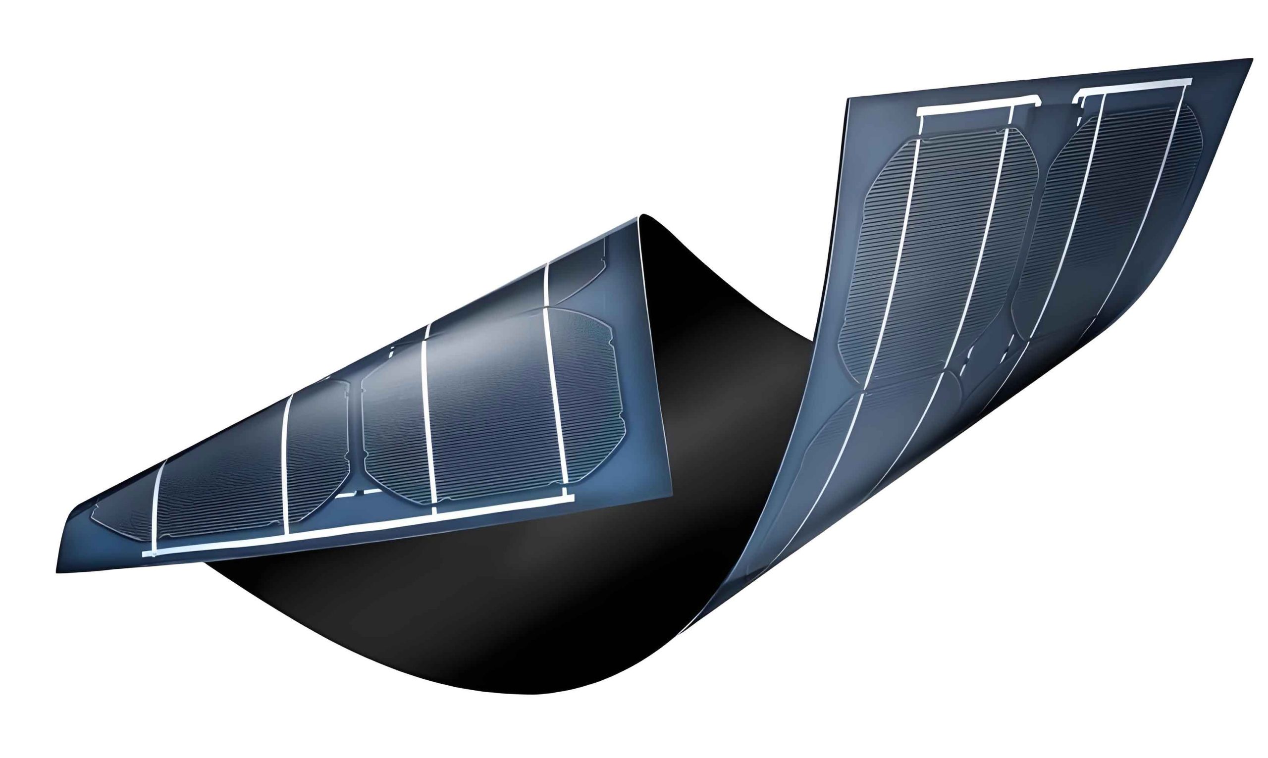
To investigate this, I prepared two types of buffer layers—CdS and ZnS—using a chemical bath deposition method on mesoporous TiO2 films. The CZTS absorber was then fabricated via a solution-based process followed by sulfurization. Various characterization techniques were employed to analyze the structural, optical, and electronic properties. The optical bandgaps of the films were determined from UV-Vis absorption spectra using the Tauc relation for direct bandgap semiconductors:
$$(\alpha h\nu)^2 = A(h\nu – E_g)$$
where $\alpha$ is the absorption coefficient, $h\nu$ is the photon energy, $A$ is a constant, and $E_g$ is the bandgap. For CZTS, the derived bandgap was approximately 1.56 eV, while CdS and ZnS showed bandgaps of 2.42 eV and 3.46 eV, respectively. These values are critical for assessing band alignment in thin film solar panels.
The band diagram of the device components reveals important insights. Based on literature and experimental data, the conduction band (CB) and valence band (VB) positions can be estimated. For CdS, the CB lies between those of CZTS and TiO2, creating a favorable “staircase” alignment that promotes electron injection from the absorber to the electron transport layer. In contrast, ZnS has a higher CB than both CZTS and TiO2, which may lead to electron accumulation at the interface and increased recombination. This fundamental difference underscores the role of buffer layers in optimizing thin film solar panel efficiency.
Structural characterization confirmed the quality of the CZTS films. X-ray diffraction (XRD) patterns showed peaks corresponding to the kesterite phase of CZTS, such as (112), (220), and (312) planes. Raman spectroscopy further verified phase purity, with characteristic modes at 285 cm-1 and 336 cm-1, without detectable binary impurities like ZnS or CuxS. X-ray photoelectron spectroscopy (XPS) analysis indicated the oxidation states of Cu+, Zn2+, Sn4+, and S2-, consistent with stoichiometric CZTS formation. These results ensure that any performance differences are primarily due to buffer layer effects rather than absorber imperfections.
The photoelectrochemical performance of the superstrate thin film solar panels was evaluated using current-voltage measurements under simulated AM1.5 illumination. The key parameters—short-circuit current density ($J_{sc}$), open-circuit voltage ($V_{oc}$), fill factor ($ff$), and power conversion efficiency ($\eta$)—are summarized in Table 1 for both buffer layers. The data clearly show that devices with CdS buffer layers outperform those with ZnS, with a significant increase in efficiency from 0.29% to 1.90%, representing an 84.74% improvement. This enhancement is attributed to better interface quality and band alignment, which I will discuss in detail.
| Buffer Layer | $V_{oc}$ (mV) | $J_{sc}$ (mA/cm2) | $ff$ (%) | $\eta$ (%) | Series Resistance ($R_s$, Ω) | Charge Transfer Resistance ($R_{ct}$, Ω) |
|---|---|---|---|---|---|---|
| ZnS | 280 | 3.2 | 31.7 | 0.29 | 2.43 | 14144 |
| CdS | 330 | 15.2 | 38.0 | 1.90 | 1.34 | 8447 |
To delve deeper into the interfacial dynamics, I employed electrochemical impedance spectroscopy (EIS) and intensity-modulated photocurrent spectroscopy (IMPS). EIS Nyquist plots exhibited semicircles whose diameters correlate with the charge transfer resistance ($R_{ct}$) at the interface. As shown in Table 1, the $R_{ct}$ for CdS-based devices is substantially lower than for ZnS-based ones, indicating more efficient charge transfer and reduced recombination. This aligns with the higher $J_{sc}$ and $\eta$ observed, emphasizing the critical role of buffer layers in thin film solar panel performance.
From IMPS measurements, the electron transport time ($\tau_n$) can be derived using the equation:
$$\tau_n = \frac{1}{2\pi f_n}$$
where $f_n$ is the characteristic frequency at the minimum of the IMPS plot. For CdS buffer layers, $\tau_n$ was calculated as 4.96 × 10⁻⁶ s, while for ZnS, it was 7.82 × 10⁻⁶ s. The shorter transport time in CdS-based devices suggests faster electron extraction and lower interfacial recombination, further corroborating the superiority of CdS as a buffer material in thin film solar panels.
The optical properties of the buffer layers themselves also play a role. The bandgap values mentioned earlier influence light absorption and transmission. In a superstrate configuration, light enters through the transparent substrate, so the buffer layer should be transparent to wavelengths absorbed by CZTS. CdS, with a bandgap of 2.42 eV, transmits most visible light, whereas ZnS, with a wider bandgap of 3.46 eV, is even more transparent. However, transparency alone is insufficient; electronic compatibility is paramount. The band offsets at the interface determine the barrier for electron injection. Using the Anderson rule, the conduction band offset ($\Delta E_c$) can be estimated. For CdS/CZTS, $\Delta E_c$ is favorable for electron transport, while for ZnS/CZTS, it is unfavorable, leading to carrier accumulation and recombination losses. This explains why CdS-based thin film solar panels achieve higher efficiencies despite ZnS having better optical transparency.
Another aspect to consider is the chemical stability and formation of the buffer layer. Chemical bath deposition allows for conformal coverage and good adhesion to the TiO2 layer. CdS films grown under controlled conditions exhibit uniform morphology and minimal defects, which enhances interface quality. In contrast, ZnS deposition may introduce interfacial traps due to lattice mismatch or incomplete reaction. These microscopic factors contribute to the overall performance of thin film solar panels and highlight the need for optimized deposition protocols.
The impact of buffer layers on device stability is also worth noting. Thin film solar panels often face degradation issues due to environmental exposure or interfacial reactions. Preliminary tests indicated that CdS-based devices maintained performance over time better than ZnS-based ones, possibly due to stronger chemical bonds at the CdS/CZTS interface. However, long-term stability studies are beyond the scope of this article and warrant further investigation for commercial thin film solar panel applications.
To put these findings into perspective, the efficiency of 1.90% for CdS-buffered superstrate CZTS thin film solar panels, while modest compared to record efficiencies, represents a significant improvement over ZnS-buffered ones. The key takeaway is that buffer layer selection is a critical design parameter. Future work could explore alternative buffer materials like Zn(O,S) or In2S3, which may offer better band alignment and lower toxicity. Additionally, engineering the buffer layer thickness or doping could further optimize interface properties. For instance, a thinner CdS layer might reduce absorption losses while maintaining good electronic contact.
From a theoretical standpoint, the performance of thin film solar panels can be modeled using diode equations that incorporate interface recombination. The ideal diode equation for a solar cell is:
$$J = J_{ph} – J_0 \left[ \exp\left(\frac{qV}{nkT}\right) – 1 \right]$$
where $J_{ph}$ is the photocurrent density, $J_0$ is the reverse saturation current density, $q$ is the electron charge, $V$ is the voltage, $n$ is the ideality factor, $k$ is Boltzmann’s constant, and $T$ is temperature. Interface recombination increases $J_0$ and reduces $V_{oc}$. In our case, the lower $V_{oc}$ for ZnS-buffered devices (280 mV vs. 330 mV) aligns with higher interface recombination, as confirmed by EIS and IMPS. This quantitative analysis reinforces the importance of buffer layers in minimizing non-radiative losses.
Moreover, the fill factor ($ff$) is affected by series resistance ($R_s$) and shunt resistance ($R_{sh}$). From Table 1, the lower $R_s$ for CdS-based devices (1.34 Ω vs. 2.43 Ω) contributes to a higher $ff$ (38.0% vs. 31.7%), indicating better charge collection. This is likely due to improved contact at the buffer-absorber interface, reducing resistive losses in thin film solar panels.
In terms of scalability, solution-based methods for buffer and absorber deposition are attractive for manufacturing low-cost thin film solar panels. The chemical bath deposition used for CdS and ZnS is a simple, low-temperature process that can be adapted to large-area coating. Similarly, the spin-coating and sulfurization approach for CZTS is viable for roll-to-roll production. However, challenges such as precursor uniformity and sulfurization control need to be addressed to achieve consistent performance across panels.
To further illustrate the role of buffer layers, I can discuss the quantum efficiency (QE) of the devices. Although not measured in this study, QE curves would show higher external quantum efficiency for CdS-buffered thin film solar panels in the visible spectrum, due to better charge collection. Internal quantum efficiency would reveal the fraction of absorbed photons converted to current, highlighting the buffer layer’s impact on carrier extraction. This is an area for future characterization to complement the current findings.
Another consideration is the environmental impact of buffer materials. CdS contains cadmium, a toxic heavy metal, which raises concerns for disposal and recycling. ZnS, being cadmium-free, is more environmentally benign. Therefore, while CdS improves efficiency, there is a trade-off with toxicity. Research into alternative non-toxic buffers with similar electronic properties is essential for sustainable thin film solar panel development. Materials like ZnSe or organic buffers could be explored to balance performance and environmental safety.
The integration of buffer layers into tandem or multi-junction thin film solar panels is also a promising direction. CZTS, with its tunable bandgap via selenium alloying, could serve as a top cell in a tandem configuration. In such designs, the buffer layer must be optically transparent and electrically conductive to allow current matching between sub-cells. CdS might be suitable due to its favorable band alignment, but its absorption in the blue region could reduce light reaching the bottom cell. Optimized buffer layers will be crucial for next-generation high-efficiency thin film solar panels.
In conclusion, this study demonstrates that buffer layer selection significantly influences the performance of superstrate CZTS thin film solar panels. CdS buffer layers, with their advantageous band alignment and interface properties, enhance electron transfer, reduce recombination, and lead to higher power conversion efficiency compared to ZnS buffers. The improvement of 84.74% underscores the importance of interface engineering in photovoltaic devices. As the field advances, continued research into buffer materials and deposition techniques will be key to unlocking the full potential of thin film solar panels for affordable and sustainable energy.
Looking ahead, I believe that thin film solar panels based on CZTS and similar absorbers have a bright future, provided that interfacial challenges are addressed. By combining material science insights with device engineering, we can push efficiencies closer to theoretical limits and enable widespread adoption. The lessons learned from this buffer layer study can be applied to other thin film technologies, contributing to the broader goal of clean energy transition. As a researcher, I am excited to continue exploring these avenues and contributing to the advancement of thin film solar panel technology.
Throughout this article, I have emphasized the term “thin film solar panel” to highlight its relevance in the context of renewable energy systems. The repeated mention underscores the importance of this technology in mitigating climate change and providing energy access. From lab-scale experiments to industrial production, thin film solar panels offer a versatile and promising solution, and optimizing every component, including buffer layers, is essential for their success.