
In my research on photovoltaic (PV) power conversion systems, I have explored various types of solar inverter topologies to address the challenges of efficiency, reliability, and cost. The most common types of solar inverter include string inverters, central inverters, and micro-inverters. Each type has distinct advantages and limitations. String inverters are widely used in residential and commercial installations due to their simplicity and low cost, but they suffer from partial shading losses and require large electrolytic capacitors for power decoupling, which reduces system lifetime. Central inverters are suitable for large-scale utility plants but are bulky and less flexible. Micro-inverters, on the other hand, are attached to individual PV modules, enabling module-level MPPT (Maximum Power Point Tracking) and eliminating mismatch losses. However, traditional micro-inverters often rely on electrolytic capacitors to buffer the double-line-frequency power pulsation, leading to limited lifespan. To overcome these drawbacks, I have studied a novel flyback micro-inverter that integrates active clamp and power decoupling circuits. This topology not only reduces the input filter capacitance but also achieves zero-voltage switching (ZVS) for the main switch, thereby improving efficiency and reliability. In this article, I will systematically review the different types of solar inverter, emphasize the role of power decoupling and soft-switching techniques, and present the detailed analysis of the proposed active clamp power decoupling flyback micro-inverter.
1. Overview of Types of Solar Inverter
Solar inverters are essential components that convert the DC power generated by PV modules into AC power suitable for grid connection or stand-alone loads. Based on the configuration and power level, the types of solar inverter can be classified into three main categories: central inverters, string inverters, and module-level (micro) inverters. Table 1 summarizes the key characteristics of each type.
| Feature | Central Inverter | String Inverter | Micro-Inverter |
|---|---|---|---|
| Power Range | 100 kW – 10 MW | 1 kW – 100 kW | 200 W – 1 kW |
| Efficiency | 96% – 98% | 95% – 97% | 90% – 95% |
| Lifetime | 10 – 15 years | 10 – 15 years | 15 – 25 years (with film capacitors) |
| MPPT per Panel | No | Per string | Yes |
| Power Decoupling Method | Electrolytic capacitor | Electrolytic capacitor | Active/passive circuits |
| Size and Weight | Large | Medium | Small |
| Application | Utility-scale | Residential & commercial | Residential, module-level |
Among these types, micro-inverters have gained significant attention in distributed PV systems because of their high energy yield in partial shading conditions and inherent safety (low DC voltage). However, the double-line-frequency power pulsation at the output of a single-phase inverter requires a large energy storage element to decouple the instantaneous power difference between the PV panel (constant power) and the AC grid (sinusoidal power). Traditionally, electrolytic capacitors are used, but they have limited lifespan (typically 1000–5000 hours at high temperature). To improve reliability, various power decoupling techniques have been proposed, which allow the use of long-life film capacitors. I will now discuss the power decoupling principle and how it influences the design of different types of solar inverter.
2. Power Decoupling in Single-Phase Inverters
In a single-phase grid-connected inverter, the instantaneous output power is given by:
$$ p_{\text{ac}}(t) = V_{\text{rms}} I_{\text{rms}} \left[1 – \cos(2\omega t)\right] $$
where \( V_{\text{rms}} \) and \( I_{\text{rms}} \) are the root-mean-square voltage and current, and \( \omega \) is the grid angular frequency. The PV panel, on the other hand, delivers a constant power \( P_{\text{pv}} \). To balance the power difference, an energy storage element must absorb or release the double-frequency ripple energy. The required energy storage capacity \( E \) over half a grid cycle is:
$$ E = 2 \int_{0}^{T/4} (P_{\text{pv}} – p_{\text{ac}}(t)) \, dt = \frac{P_{\text{pv}}}{\omega} $$
Hence, the necessary capacitance \( C \) is inversely proportional to the allowed voltage ripple \( \Delta V \) and the average voltage \( V_{\text{avg}} \):
$$ C = \frac{P_{\text{pv}}}{\omega \, V_{\text{avg}} \, \Delta V} $$
For a typical 80 W micro-inverter with \( V_{\text{avg}} = 210 \) V and \( \Delta V = 33 \) V, the required capacitance is only about 40 μF, which can be implemented with a long-life film capacitor. This is significantly smaller than the hundreds or thousands of microfarads needed in conventional designs with electrolytic capacitors. In the proposed flyback micro-inverter, I integrate an active clamp circuit that also serves as a power decoupling unit, thereby reducing component count and enabling soft-switching.
3. Proposed Active Clamp Power Decoupling Flyback Micro-Inverter
The topology I present is a flyback-based micro-inverter with an active clamp circuit combined with a power decoupling function. It consists of a flyback transformer with multiple windings, a main switch \( Q_1 \), auxiliary switches \( Q_2 \), \( Q_3 \), \( Q_4 \), clamp switches \( Q_5 \), \( Q_6 \), a storage capacitor \( C_s \), and output filter. The circuit diagram is shown conceptually, but due to text limitations, I will describe its operation.
The key feature is that the storage capacitor \( C_s \) serves both as a clamp capacitor to absorb the transformer leakage energy and as a power decoupling capacitor to buffer the double-line-frequency ripple. The auxiliary winding \( w_2 \) and switch \( Q_2 \) enable power flow between \( C_s \) and the primary side during the discharging phase. The operation is divided into two modes depending on whether the instantaneous PV power is greater or less than the AC output power.
3.1 Mode I: \( P_{\text{pv}} > P_{\text{ac}} \) (Excess power stored)
During this mode, the main switch \( Q_1 \) is turned on with ZVS. Energy is stored in the magnetizing inductance \( L_m \). When \( Q_1 \) is turned off, the leakage inductance energy charges \( C_s \) through the body diode of \( Q_5 \). Subsequently, the secondary winding delivers power to the grid via diode \( D_2 \) and switch \( Q_3 \). The excess energy is stored in \( C_s \). The key waveforms are shown in Figure 2 of the original paper (not reproduced here). The clamp switch \( Q_5 \) is turned on to reset the leakage energy and later turned off to allow resonance that achieves ZVS for \( Q_1 \).
3.2 Mode II: \( P_{\text{pv}} < P_{\text{ac}} \) (Deficient power supplied by \( C_s \))
In this mode, after \( Q_1 \) is turned off, the switch \( Q_2 \) is turned on instead of the secondary diode. The storage capacitor \( C_s \) discharges through the auxiliary winding \( w_2 \) to the magnetizing inductance, providing additional energy. Then the secondary side delivers the total required energy to the grid. The process ensures that the input current from the PV panel remains nearly constant with low ripple.
3.3 Zero-Voltage Switching Condition
To achieve ZVS for the main switch \( Q_1 \), the energy stored in the leakage inductance \( L_k \) must be sufficient to discharge the parasitic capacitance \( C_{ds1} \) of \( Q_1 \). The required condition is:
$$ \frac{1}{2} L_k i_{\text{reverse}}^2 \geq \frac{1}{2} C_{ds1} (v_{\text{pv}} + v_{C_s})^2 $$
where \( i_{\text{reverse}} \) is the reverse current in the leakage inductance built by the clamp circuit. The dead-time \( t_{\text{dead}} \) must satisfy:
$$ t_{\text{dead}} \geq \frac{\pi}{2} \sqrt{L_k C_{ds1}} $$
By proper design of the clamp switch \( Q_5 \) and auxiliary switch \( Q_6 \), I ensure that \( Q_1 \) always turns on with zero voltage across it, reducing switching losses and EMI.
4. Control Strategy
The control system for the proposed micro-inverter is based on digital implementation using an STM32F407 microcontroller. The block diagram is shown in Figure 6 of the original paper. The key control parameters are the peak currents \( i_{\text{peak1}} \) and \( i_{\text{peak2}} \) defined as:
$$ i_{\text{peak1}} = \sqrt{\frac{2 P_{\text{pv}} T_s}{L_m}} $$
$$ i_{\text{peak2}} = \sqrt{\frac{P_{\text{pv}} T_s}{L_m}} \cdot 2 |\sin(\omega t)| $$
where \( T_s \) is the switching period. The duty cycle of the main switch \( d_1 \) is adjusted by an input current loop. The duty cycles for the power decoupling switches are derived from energy balance equations:
$$ d_{\text{ch}} T_s = \frac{L_m (i_{\text{peak1}} – i_{\text{peak2}})}{v_{C_s}} \quad \text{(Mode I charging)} $$
$$ d_{\text{dis}} T_s = \frac{L_m (i_{\text{peak2}} – i_{\text{peak1}})}{v_{C_s}} \cdot \frac{n_2}{n_1} \quad \text{(Mode II discharging)} $$
Additionally, a voltage loop regulates the average voltage of \( C_s \) to a reference value (e.g., 210 V) by slightly adjusting \( i_{\text{peak1}} \) to maintain power balance. The grid-side switches \( Q_3 \) and \( Q_4 \) commutate at grid frequency, while the clamp switches \( Q_5 \) and \( Q_6 \) operate with fixed timing to achieve ZVS.
5. Design Considerations and Component Selection
I have derived design equations for the key components. Table 2 lists the parameters used in my 80 W prototype.
| Parameter | Value |
|---|---|
| Input Voltage \( v_{\text{pv}} \) | 50 V |
| AC Voltage (rms) | 110 V |
| Rated Power | 80 W |
| Switching Frequency \( f_s \) | 50 kHz |
| Transformer Turns Ratio \( n_1:n_2:n_3:n_4 \) | 1:1:1.1:1.1 |
| Magnetizing Inductance \( L_m \) | 60 μH |
| Leakage Inductance \( L_k \) | 5.5 μH |
| Storage Capacitor \( C_s \) | 40 μF (film) |
| Input Filter Capacitor \( C_{\text{in}} \) | 6.8 μF (film) |
| Main Switch \( Q_1 \) | NCE65T260F |
| Clamp Switches \( Q_5, Q_6 \) | CI19N120SM |
| Decoupling Switch \( Q_2 \) | MS15N100HGT1 |
| Grid Switches \( Q_3, Q_4 \) | NCE70T180F |
| Diodes \( D_1, D_2, D_3 \) | DSEI30-10A |
I chose the storage capacitor value based on the required energy buffering. From equation (10) in the original paper: \( C_s = \frac{P_{\text{pv}}}{\omega V_{C_s} \Delta V_{C_s}} \). With \( P_{\text{pv}}=80 \) W, \( V_{C_s}=210 \) V, \( \Delta V_{C_s}=33 \) V, and \( \omega=2\pi\times 50 \) rad/s, we get \( C_s \approx 36.8 \) μF, so I used 40 μF for margin. The magnetizing inductance must satisfy DCM condition. Using equation (12) and constraints, I set \( L_m = 60 \) μH.
6. Simulation and Experimental Results
I built an 80 W prototype and performed both simulation (using PSIM) and hardware experiments. Figure 9 in the original paper shows the steady-state waveforms: the AC output current is sinusoidal and in phase with the grid voltage, while the PV input current ripple is below 10%, confirming effective power decoupling. The storage capacitor voltage ripples around 210 V with ±33 V variation, matching the design.
Figure 11 demonstrates ZVS of the main switch: the drain-source voltage \( v_{ds1} \) falls to zero before the gate drive signal goes high. This operation reduces switching losses significantly. The measured efficiency curve in Figure 17 shows a peak efficiency of 81% at around 60 W load, and the proposed topology improves efficiency by about 1.6% on average compared to a version without active clamp.
Table 3 compares the proposed inverter with other flyback micro-inverters reported in literature.
| Reference | Rated Power (W) | Input Voltage (V) | Number of Switches | Filter Capacitor (μF) | Auxiliary Capacitor (μF) | Peak Efficiency (%) |
|---|---|---|---|---|---|---|
| [13] | 100 | 35 | 7 | 20 | 40 | 70 |
| [14] | 100 | 35 | 8 | 15 | 44 | 73 |
| [21] | 80 | 50 | 7 | 560 | – | 82.3 |
| Proposed | 80 | 50 | 9 | 6.8 | 40 | 81 |
While the proposed inverter uses two more switches than some designs, the input filter capacitor is drastically reduced from 560 μF (electrolytic) to 6.8 μF (film), and the auxiliary capacitor is a long-life film capacitor of 40 μF. This leads to a much longer lifetime. The efficiency is competitive, and the ZVS operation reduces electromagnetic interference.
7. Conclusion
Through this research, I have demonstrated that by integrating an active clamp circuit with a power decoupling function into a flyback micro-inverter, it is possible to achieve high reliability (using film capacitors) and high efficiency (through ZVS). The proposed topology effectively addresses the limitations of conventional types of solar inverter that rely on electrolytic capacitors. The key to success is the dual use of the storage capacitor as a clamp capacitor, reducing component count. The design methodology and control strategy are validated by simulation and experiments. As the demand for long-lasting and efficient types of solar inverter grows, the proposed micro-inverter offers a promising solution for module-level power conversion in distributed PV systems.
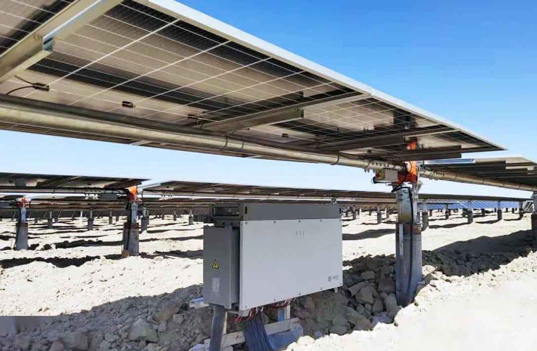
In the figure above, a typical string inverter configuration is illustrated, representing one of the major types of solar inverter used in residential applications. Future work will focus on further improving the efficiency by optimizing the magnetic design and reducing conduction losses in the auxiliary switches.