
The quest for sustainable and scalable photovoltaic technology has long been a central focus of my research. While silicon dominates the market, the promise of thin film solar panels—with their potential for lower material usage, flexibility, and reduced manufacturing energy—has driven intensive investigation into alternative absorber materials. For years, the landscape was defined by compounds like cadmium telluride (CdTe) and copper indium gallium selenide (CIGS). However, the toxicity of cadmium and the critical scarcity of tellurium and indium cast a shadow over their long-term, global deployment potential. This fundamental materials challenge prompted a search for truly earth-abundant, benign alternatives. Copper zinc tin sulfoselenide (CZTSSe) emerged as a promising candidate, yet its complex quinary chemistry introduces significant hurdles in phase stability and defect control, ultimately limiting efficiency gains. It was within this context of seeking a simpler, greener, and high-performance solution that our attention turned decisively to the binary compound germanium selenide (GeSe).
From a fundamental materials perspective, GeSe presents an exceptionally compelling portfolio of properties for thin film solar panel applications. Its optimal bandgap of approximately 1.14 eV sits close to the Shockley-Queisser ideal for single-junction devices, enabling efficient harvesting of the solar spectrum. The absorption coefficient is high, exceeding \(10^4\) cm\(^{-1}\), meaning a film merely 1–2 microns thick can absorb most incident sunlight, a key advantage for any thin film solar panel technology aiming to minimize material use. Perhaps most striking is its high carrier mobility, reported to be around 128 cm2 V-1 s-1, which is orders of magnitude higher than many polycrystalline chalcogenide absorbers. This combination suggests a theoretical efficiency ceiling well above 30%, rivaling and even potentially surpassing established technologies. The journey from this theoretical promise to a functional device, however, hinges entirely on the ability to deposit high-quality, phase-pure GeSe thin films—a challenge that had stymied prior efforts.
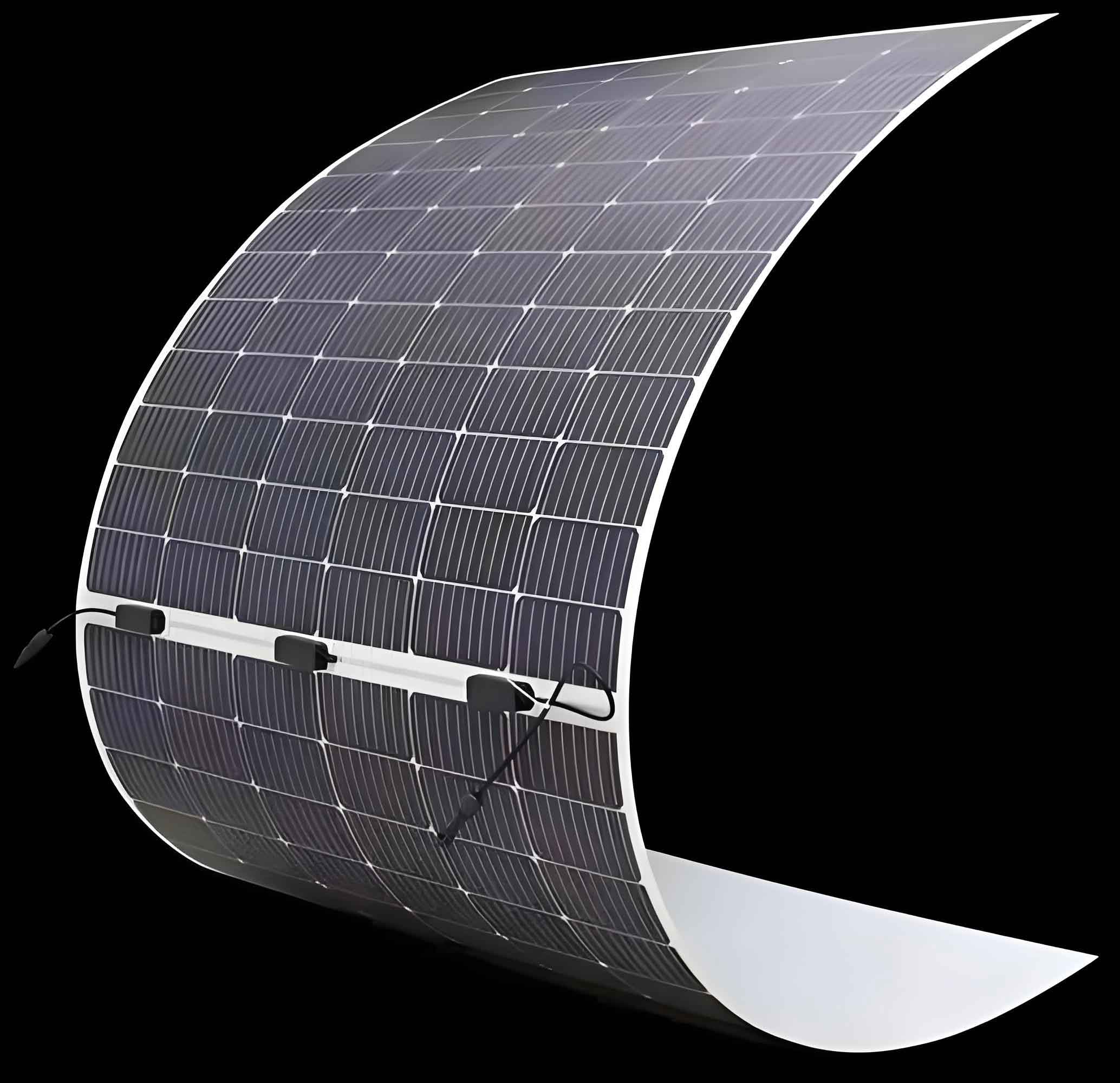
The principal obstacle in synthesizing GeSe films lies in its narrow thermodynamic stability window. During conventional deposition processes, undesirable secondary phases like elemental germanium (Ge) or germanium diselenide (GeSe2) readily form. These phases act as recombination centers or create unwanted band alignments, severely degrading the electronic quality of the absorber layer and crippling the performance of any resulting thin film solar panel. Our breakthrough came from reconceptualizing the problem: instead of fighting GeSe’s intrinsic properties, we decided to leverage them. We noted that GeSe possesses a remarkably high saturated vapor pressure at moderate temperatures and, crucially, sublimes as diatomic GeSe molecules. This insight led us to pioneer a novel deposition technique we termed Rapid Thermal Sublimation (RTS).
The RTS process is elegantly self-regulating. A source containing GeSe powder (which may initially contain impurities or off-stoichiometry) is rapidly heated in a vacuum. The species with the highest vapor pressure at the set temperature sublimates first. By carefully selecting the temperature regime, we operate in a window where the equilibrium vapor pressure of GeSe significantly exceeds that of Ge or GeSe2. The vapor pressure ratio dictates the purification efficacy. We can express the partial pressure of a component *i* using the Clausius-Clapeyron relation:
$$ \ln P_i = A – \frac{\Delta H_{subl,i}}{RT} $$
where \( \Delta H_{subl,i} \) is the enthalpy of sublimation, *R* is the gas constant, *T* is the temperature, and *A* is a constant. For a binary compound like GeSe subliming congruently as GeSe(g), the process is described by the equilibrium:
$$ \text{GeSe(s)} \rightleftharpoons \text{GeSe(g)} $$
The sublimation flux, *J*, which determines the film growth rate, is given by the Hertz-Knudsen equation:
$$ J = \alpha \frac{(P_{eq} – P_{amb})}{\sqrt{2 \pi M k_B T}} $$
where \( P_{eq} \) is the equilibrium vapor pressure of GeSe at the source temperature, \( P_{amb} \) is the ambient pressure (near zero in our vacuum chamber), *M* is the molecular mass of GeSe, \( k_B \) is Boltzmann’s constant, and \( \alpha \) is the sticking coefficient (close to 1 for a condensing film). The high \( P_{eq} \) of GeSe directly enables the astonishing growth rates we achieved—up to 4.8 µm min-1. This is not merely a manufacturing advantage; it has profound implications for defect formation. The rapid transfer of GeSe molecules from the vapor phase to the growing film surface minimizes the time atoms have to diffuse into wrong lattice sites, thereby suppressing the formation of detrimental point defects like cation-anion anti-sites (GeSe or SeGe) or vacancies, which are common culprits of non-radiative recombination in thin film solar panel absorbers.
| Material | Bandgap (eV) | Absorption Coefficient (cm-1) at α > 104 | Hole Mobility (cm2 V-1 s-1) | Elemental Abundance & Toxicity | Record Lab Efficiency (%) |
|---|---|---|---|---|---|
| GeSe (This Work) | ~1.14 | >104 (at ~1.3 eV) | ~128 | Abundant, Low Toxicity | 1.48 (Initial report) |
| CdTe | ~1.45 | >104 | ~10-80 | Te: Scarce, Cd: Toxic | ~22.1 |
| CIGS | ~1.0-1.7 (tunable) | >104 | ~10-100 | In, Ga: Scarce | ~23.6 |
| CZTSSe | ~1.0-1.5 | >104 | < 10 | Abundant, Low Toxicity | ~12.6 |
| a-Si:H | ~1.7 | >104 (at higher E) | ~1 | Abundant | ~14.0 |
We fabricated our first-generation thin film solar panel devices in a simple substrate configuration: glass/Mo/GeSe/CdS/i-ZnO/ITO. The Mo back contact was deposited by sputtering. The heart of the device, the GeSe absorber layer with a thickness of approximately 1.5 µm, was deposited via the RTS technique. A thin n-type cadmium sulfide (CdS) buffer layer (~50 nm) was then deposited by chemical bath deposition, followed by sputtered i-ZnO and indium tin oxide (ITO) as the transparent conductive front electrode. This structure yielded a power conversion efficiency (PCE) of 1.48%, which, while modest, constituted the first-ever report of photovoltaic activity from a GeSe-based thin film solar panel. The current-voltage characteristics under standard AM 1.5G illumination revealed the primary limitations: a relatively low short-circuit current density (\(J_{sc}\)) and fill factor (FF). These metrics pointed directly to non-optimal carrier collection, likely due to interface recombination at the GeSe/CdS heterojunction and the presence of bulk defects that persisted despite the improved film quality from RTS.
The analysis of the device physics provides a clear roadmap for improvement. The open-circuit voltage (\(V_{oc}\)) is fundamentally limited by recombination and can be expressed as:
$$ V_{oc} = \frac{E_g}{q} – \frac{n k_B T}{q} \ln\left(\frac{J_{00}}{J_{sc}}\right) $$
where \(E_g\) is the absorber bandgap, \(q\) is the elementary charge, \(n\) is the diode ideality factor, and \(J_{00}\) is the reverse saturation current prefactor. A high \(J_{00}\), driven by Shockley-Read-Hall recombination via defect states in the bulk or at interfaces, directly reduces \(V_{oc}\). Similarly, the fill factor is degraded by high series resistance (\(R_s\)) and low shunt resistance (\(R_{sh}\)). For our initial devices, we identified the following key areas for optimization to elevate the performance of the GeSe thin film solar panel:
- Absorber Quality: Further refining the RTS process parameters (source temperature, substrate temperature, deposition pressure) to enhance grain growth and reduce point defect density. Post-deposition annealing in controlled Se or Ge vapor atmospheres could be explored to fine-tune stoichiometry and passivate grain boundaries.
- Heterojunction Engineering: The CdS buffer layer, while common, has a band alignment with GeSe that may not be ideal. We need to investigate alternative buffer/window materials (e.g., Zn(O,S), (Zn,Mg)O, or TiO2) to achieve a more favorable conduction band offset, minimize interface defect density, and reduce parasitic absorption.
- Device Architecture: Transitioning from a substrate to a superstrate configuration (where light enters through the transparent front contact) could be beneficial. This might involve developing a suitable transparent and stable back contact for GeSe or exploring bifacial designs.
| Defect Type | Likely Origin | Impact on Device | Potential Mitigation via RTS & Processing |
|---|---|---|---|
| GeSe Anti-site (Donor) | Off-stoichiometry (Ge-rich) | Compensation, reduces p-type conductivity, recombination center | Self-purification via vapor pressure difference; Se-rich annealing |
| SeGe Anti-site (Acceptor) | Off-stoichiometry (Se-rich) | May enhance p-type doping but can be a deep trap | Self-purification; precise temperature control during RTS |
| VSe (Donor) | Se deficiency during growth | Shallow donor, compensates acceptors | Rapid condensation reduces time for vacancy formation; post-selenization |
| VGe (Acceptor) | Ge deficiency | Deep acceptor, strong recombination center | Congruent sublimation of GeSe minimizes Ge loss; Ge-vapor annealing |
| Grain Boundary Defects | Film nucleation & growth | Recombination, trapping, barrier to carrier transport | Optimizing substrate temperature to promote lateral grain growth; seed layers |
Beyond efficiency, a critical benchmark for any new photovoltaic technology is operational stability. Here, our GeSe thin film solar panel exhibited remarkably promising behavior. Unencapsulated devices stored in ambient air (with typical fluctuations in temperature and humidity) showed negligible degradation in performance over nearly two months. This intrinsic stability likely stems from the chemically robust nature of the GeSe compound itself. Unlike hybrid perovskites, it is not susceptible to moisture-induced decomposition. Unlike some chalcogenides, it does not readily oxidize under normal atmospheric conditions. This robustness is a monumental practical advantage, significantly reducing the complexity and cost of module packaging and extending the operational lifetime, which are vital considerations for the commercial viability of a thin film solar panel technology.
Scaling the RTS process from lab-scale to industrial manufacturing is a crucial next step. The technique’s inherent characteristics are highly favorable. The fast deposition rate (4.8 µm min-1) translates directly to high throughput, a key metric for reducing the cost per watt of a thin film solar panel. The self-purifying nature of the sublimation process relaxes the purity requirements for the source material, potentially lowering raw material costs. We envision a scalable RTS system involving a linear source or multiple crucibles moving relative to a large-area substrate under vacuum, a concept analogous to processes used for other sublimated materials. The thermal budget is confined to heating the source and optionally the substrate, which could be more energy-efficient than the sustained high-temperature processing required for some other compound semiconductors.
The future research pathway for GeSe thin film solar panels is multidimensional and rich with opportunity. Our initial work has merely opened the door. A systematic materials science campaign is needed to fully map the phase diagram, defect chemistry, and doping limits of GeSe. Can it be effectively doped n-type to enable homojunctions? What is the true nature of the dominant point defects, and can they be passivated? Concurrently, device engineering must advance. We plan to explore bandgap engineering through alloying, perhaps with sulfur (forming GeSe1-xSx) to widen the bandgap for better \(V_{oc}\) or with tin (Sn) for bandgap narrowing or structural modification. The development of low-resistivity, ohmic back contacts tailored to GeSe is another essential task. Furthermore, integrating the GeSe absorber into tandem cell architectures, either with a wider-bandgap top cell (like a perovskite) or as the bottom cell beneath a silicon cell, could leverage its ideal infrared response to push efficiencies toward and beyond 30%.
| Development Phase | Key Focus Areas | Expected Efficiency Range (%) | Critical Challenges |
|---|---|---|---|
| Phase 1: Proof-of-Concept (Current) | Demonstrate PV effect; basic device fabrication; initial stability test. | 1 – 3 | Film purity, primitive device structure, unoptimized interfaces. |
| Phase 2: Materials Optimization | Defect control via RTS refinement; stoichiometry tuning; grain growth. | 5 – 10 | Understanding and mitigating dominant recombination pathways. |
| Phase 3: Device Engineering | Advanced buffer/window layers; contact optimization; superstrate design. | 10 – 15 | Achieving optimal band alignment and low interface recombination. |
| Phase 4: Advanced Concepts | Bandgap engineering (alloying); surface passivation; tandem integration. | 15 – 20+ | Material stability under alloying; process integration for tandems. |
| Phase 5: Commercial Prototyping | Scalable deposition (roll-to-roll, large-area RTS); module fabrication; reliability testing. | > 15 (module) | Scaling uniformity, manufacturing yield, cost reduction, certification. |
In conclusion, the journey to develop a high-performance, environmentally benign, and scalable thin film solar panel technology is fraught with challenges. Our discovery and initial development of GeSe as a photovoltaic absorber marks a significant pivot towards a promising new material platform. Its binary simplicity, excellent intrinsic optoelectronic properties, demonstrated stability, and the innovative Rapid Thermal Sublimation deposition method collectively address many of the shortcomings that plague both established and emerging alternatives. While the reported efficiency is nascent, it represents a starting point from a previously unexplored direction. The fundamental attributes of GeSe provide a solid foundation upon which significant improvements can be built through dedicated materials science and device engineering. We are convinced that with systematic research into its defect physics, interface properties, and integration into advanced architectures, the efficiency of GeSe-based thin film solar panels will rise substantially. This material has the potential not just to be a new contender in the photovoltaic field, but to redefine expectations for what a sustainable, high-performance, and manufacturable thin film solar panel technology can achieve, ultimately contributing meaningfully to the global clean energy transition.