
Driven by the global ambition of “carbon peak” and “carbon neutrality,” the increasing demand for clean energy has made photovoltaic systems one of the most favored generation technologies. Among all the components of a photovoltaic system, solar inverters play the central role of converting the direct-current (DC) power from photovoltaic arrays into grid-compatible alternating-current (AC) power. However, solar inverters are also notorious sources of electromagnetic interference (EMI) because they contain multiple power electronic converters such as DC–DC boost converters, DC–AC inverters, and auxiliary power supplies. The fast switching of power semiconductor devices in these converters generates high dv/dt and di/dt transients, which produce both common-mode (CM) and differential-mode (DM) conducted EMI. In particular, common-mode conducted EMI is a dominant concern because it flows through parasitic capacitances to ground and can easily couple into the AC and DC ports, causing violation of electromagnetic compatibility (EMC) standards.
International standards such as CISPR 16 and CISPR 11 establish limits and measurement procedures for conducted emissions. For solar inverters, the conducted EMI spectrum from 150 kHz to 30 MHz must be evaluated using a line impedance stabilization network (LISN). To ensure that a given solar inverter meets these limits, accurate diagnosis of the dominant noise sources and propagation paths is essential. However, the diagnosis is complicated by the fact that solar inverters typically contain several different switching converters that operate at different frequencies and are coupled through the same DC bus and ground plane. Therefore, a multi-source diagnostic methodology is required.
In this work, I present a comprehensive study on the diagnosis and suppression of common-mode conducted EMI in high-power solar inverters. The study covers:
• the construction of an EMI test platform for a high-power solar inverter and the diagnosis of dominant interference sources and hidden propagation paths;
• the establishment of a common-mode conducted EMI model for a three-level active neutral-point-clamped (3L-ANPC) inverter, and the proposal of a balanced-bridge-based coordinated suppression strategy for both AC and DC side CM noise;
• the establishment of a common-mode conducted EMI model for a multi-output dual-switch flyback auxiliary power supply, and the application of a cancellation-capacitor technique for CM noise reduction.
All models and suppression methods are verified by simulation and experimental measurements on a 10-kW prototype solar inverter.
II. Common-Mode Conducted EMI Analysis and Diagnosis in High-Power Solar Inverters
Testing platform and structure of the solar inverter
To properly measure conducted EMI, I first built a test platform following CISPR 16. The equipment under test (EUT) is a three-phase grid-connected solar inverter with an output power of 10 kW, a DC input voltage of 540 V, and an AC line voltage of 380 V. The test platform uses a 4 m × 2 m aluminum ground plane, with the EUT placed at least 40 cm above the ground plane. Both AC and DC sides are connected through LISNs, which provide a stable radio-frequency impedance and route the noise to a spectrum analyzer or a receiver. The measurement setup also includes a four-channel oscilloscope (Rohde & Schwarz RTE1024) and high-voltage differential probes (Keysight N2891A) for time-domain waveform capture.
The solar inverter under study consists of a boost converter, a 3L-ANPC inverter, a DC-side auxiliary power supply, and an AC-side auxiliary power supply. The boost converter regulates the DC bus voltage and tracks the maximum power point of the photovoltaic array. The 3L-ANPC inverter converts the DC bus voltage into a three-phase AC voltage. The auxiliary power supplies provide isolated low-voltage rails for the control circuits, gate drivers, and sensors. Both auxiliary supplies are based on dual-switch flyback topologies. In this system, every converter module creates a distinct noise source with its own switching frequency and harmonic signature.
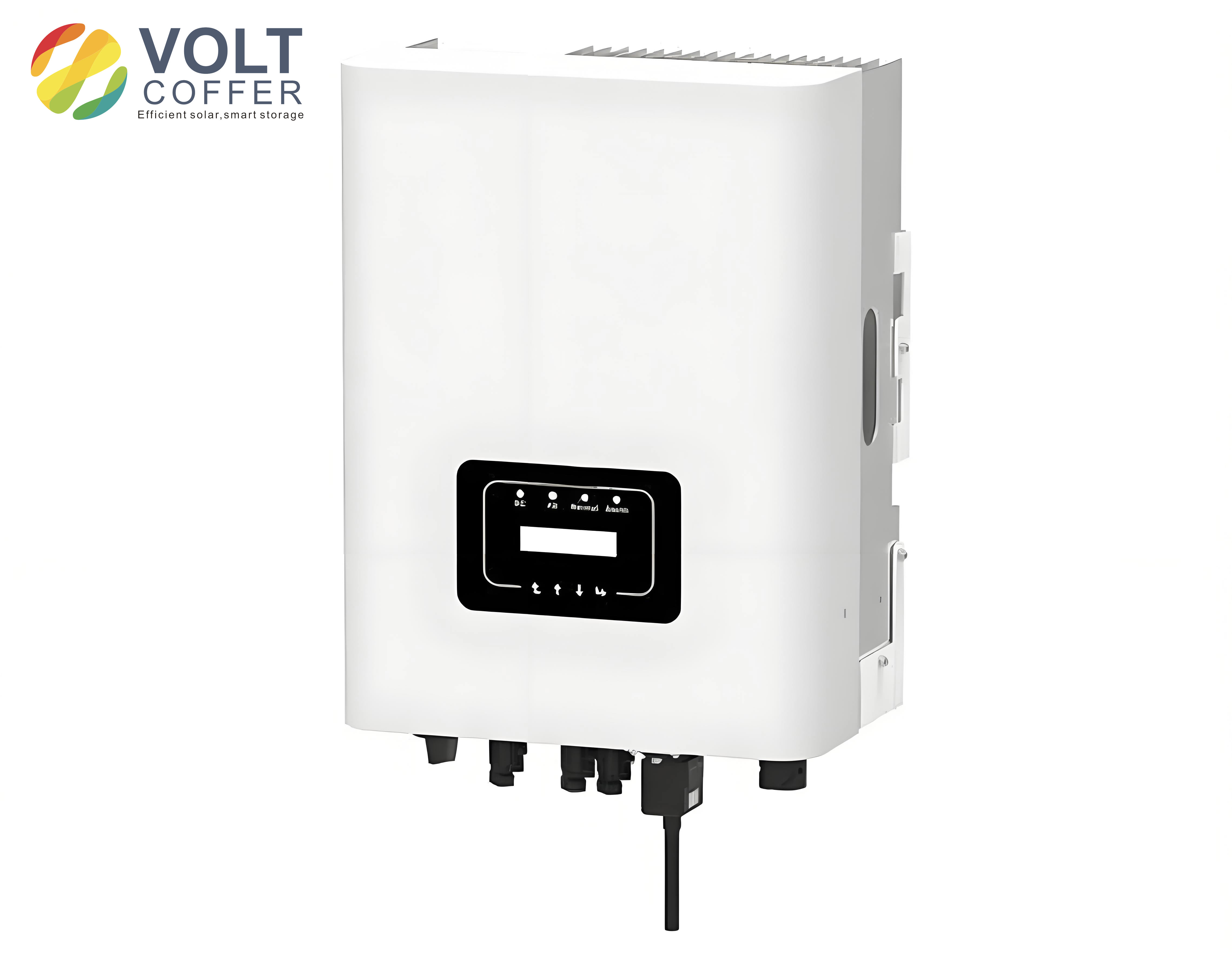
Figure 1 shows a typical high-power solar inverter module used in this study.
Measurement of interference sources
To identify which converters are the dominant EMI sources, I measured the voltage waveforms across the power switches of each converter using the high-voltage differential probes. The operating conditions are listed in Table I.
| Parameter | Value |
|---|---|
| DC bus voltage | 540 V |
| AC line voltage | 380 V |
| Output power | 10 kW |
After capturing the time-domain signals, I applied the fast Fourier transform (FFT) to obtain the frequency spectra of the four main disturbance sources. The spectra exhibit periodic peaks at the fundamental switching frequency and its harmonics. The switching frequencies of the four sources are summarized in Table II.
| Source | Switching frequency |
|---|---|
| 3L-ANPC inverter | 20.5 kHz |
| Boost converter | 18 kHz |
| DC auxiliary power supply | 93.5 kHz |
| AC auxiliary power supply | 66 kHz |
By examining the frequency spacing of the interference peaks at the AC and DC ports, I identified the dominant sources in different frequency bands. The diagnosis results are listed in Table III.
| Port | Frequency range | Dominant source |
|---|---|---|
| AC side | 150 kHz – 500 kHz | ANPC inverter |
| AC side | 500 kHz – 10 MHz | DC auxiliary power supply |
| AC side | 10 MHz – 30 MHz | ANPC inverter |
| DC side | 150 kHz – 800 kHz | ANPC inverter |
| DC side | 800 kHz – 10 MHz | DC auxiliary power supply |
| DC side | 10 MHz – 30 MHz | ANPC inverter |
This multi-source diagnostic analysis clearly indicates that the 3L-ANPC inverter and the DC auxiliary power supply are the two dominant sources of common-mode conducted EMI in this solar inverter. Consequently, the subsequent modeling and suppression efforts focus on these two converters.
Diagnosis of common-mode propagation paths
To gain a complete understanding of the common-mode EMI mechanism, I analyzed the propagation paths from each noise source to the LISNs. The system contains the following major capacitive couplings:
– the semiconductor devices in the ANPC inverter have parasitic capacitances to the grounded heatsink;
– the boost converter MOSFET and diode also have parasitic capacitances to ground;
– the flyback transformers in the auxiliary supplies exhibit inter-winding capacitances;
– the DC-side PV array has a distributed capacitance to ground, denoted as \(C_{PV}\).
Using the substitution theorem and replacing the switching devices by equivalent voltage or current sources, I constructed preliminary CM models for each converter. By combining these models with the LISN models and the EMI filters, I identified a provisional set of CM propagation paths. However, experiments revealed that two hidden paths existed and had a significant impact on the noise coupling.
The first hidden path was discovered when I increased the inductance of the AC-side CM choke \(L_{AC_CM}\). The AC-port interference from the ANPC inverter decreased significantly, but the interference from the DC auxiliary supply remained almost unchanged. This indicated that the DC auxiliary supply noise could bypass the AC-side choke. By measuring the capacitance between the nodes AGND and GRID with an impedance analyzer, I found a coupling capacitance of approximately 10 pF. A physical inspection of the printed circuit board showed that this capacitance came from the primary-to-secondary capacitance of the AC-side surge arrester. Therefore, the first hidden path is formed by the coupling capacitance \(C_{LA}\) between the auxiliary ground AGND and the grid node GRID.
The second hidden path was discovered in a similar way on the DC side. Increasing the DC-side CM choke \(L_{DC_CM}\) reduced the ANPC interference but did not affect the DC auxiliary supply interference. A measurement between AGND and PV node revealed a capacitance of about 1 nF, which was traced to the primary-to-secondary capacitance \(C_{CS}\) of the current sensor. Thus, the second hidden path is formed by the current-sensor coupling capacitance between AGND and the PV node.
Figure 2 shows the complete common-mode interference path model of the solar inverter, including these two hidden paths. This path model is essential for understanding how the auxiliary power supply noise propagates to the AC and DC ports even in the presence of common-mode chokes.
III. Balanced-Bridge-Based Coordinated Suppression of AC/DC Common-Mode EMI for a Three-Level ANPC Inverter
Topology and operation of the 3L-ANPC inverter
The 3L-ANPC inverter is a popular topology for solar inverters because it offers lower voltage stress on the switches and better harmonic performance than a two-level inverter. The topology consists of three phases, each having six switches. In the DPWM1 modulation scheme, the switching states are arranged so that the high-frequency operation is concentrated on two SiC MOSFETs in each phase, while the remaining switches are loss-optimized Si IGBTs. This hybrid SiC/Si design achieves high efficiency while keeping the cost acceptable.
For the A-phase, the three voltage jump nodes are labeled A1, A, and A2. The parasitic capacitances between each device and ground are denoted \(C_{S1G}, C_{S2G}, …, C_{S6G}\). The DC bus has two equal capacitors \(C_{X1}\) and \(C_{X2}\), and the midpoint is N. The AC-side LC filter uses an inductor \(L_{AC}\) and a capacitor bank \(C_{AC}\) with a floating midpoint O. The CM equivalent circuit is derived by replacing the devices with voltage sources and simplifying the three-phase model into a single-phase equivalent.
Common-mode interference source modeling
Using the substitution theorem, I replaced each IGBT/MOSFET with voltage or current sources according to the switching state. Since the DC bus capacitors have very low impedance at high frequencies, the current sources can be short-circuited. After this simplification, the A-phase model has three independent voltage sources \(v_{A1N}\), \(v_{A2N}\), and \(v_{AN}\). Combining the three phases, the total common-mode source is
$$v_{CM} = \frac{v_{AN} + v_{BN} + v_{CN}}{3}$$
and the two auxiliary common-mode sources are
$$v_{CM1} = \frac{v_{A1N} + v_{B1N} + v_{C1N}}{3}$$
$$v_{CM2} = \frac{v_{A2N} + v_{B2N} + v_{C2N}}{3}$$
In the DPWM1 modulation at a 50-Hz fundamental frequency, \(v_{A1N}\) and \(v_{A2N}\) change at a frequency of 50 Hz. Their high-frequency content is negligible, whereas \(v_{CM}\) switches at the carrier frequency of 20.5 kHz. Therefore, the influence of \(v_{CM1}\) and \(v_{CM2}\) on conducted EMI in the 150 kHz–30 MHz band can be ignored. The final CM noise source model is therefore a single voltage source \(v_{CM}\). The equivalent paths are represented by two lumped capacitances:
$$C_{P1} = 3 C_{S3G}$$
$$C_{P2} = 3(C_{S1G}+C_{S2G}+C_{S4G}+C_{S5G}+C_{S6G})$$
where the factor 3 arises from the three parallel phases.
To obtain accurate values for the circuit components, I measured the impedances of the inductors and capacitors with an Agilent 4294A impedance analyzer. The AC filter inductor \(L_{AC}\) was fitted with a four-stage RLC network to capture its high-frequency parasitic resonances. The fitted parameters are shown in Table IV.
| Parameter | Value | Parameter | Value |
|---|---|---|---|
| R1 | 16 kΩ | R3 | 350 Ω |
| L1 | 200 µH | L3 | 0.5 µH |
| C1 | 0.09 nF | C3 | 1.0 nF |
| R2 | 400 Ω | R4 | 200 Ω |
| L2 | 4.5 µH | L4 | 0.2 µH |
| C2 | 0.6 nF | C4 | 0.2 nF |
The AC filter capacitor \(C_{AC}\) was modeled as a series RLC circuit with \(R_{cap}=0.35\ \Omega\), \(L_{cap}=200\ \text{nH}\), and \(C_{cap}=7.9\ \mu\text{F}\).
The IGBT module’s parasitic capacitances to ground were directly measured with the impedance analyzer. The measured values are listed in Table V.
| Parameter | Value |
|---|---|
| C_S1G | 77.7 pF |
| C_S2G | 164.5 pF |
| C_S3G | 115.3 pF |
| C_S4G | 125.0 pF |
| C_S5G | 22.8 pF |
| C_S6G | 83.9 pF |
Using these values, I obtained \(C_{P1}=345.9\ \text{pF}\) and \(C_{P2}=1421.7\ \text{pF}\). These two capacitances play a key role in the balanced-bridge design.
AC balanced-bridge method
The conventional AC balanced-bridge method connects the AC filter neutral point O to the DC midpoint N through a wire with a small inductance \(L_N\). Additionally, a capacitor \(C_{BUS}\) is connected between the DC midpoint and ground to adjust the balance condition. The equivalent CM circuit can be reduced to a four-branch bridge. The bridge is balanced when
$$\frac{Z_1}{Z_2} = \frac{Z_3}{Z_4}$$
In our system, \(Z_1\) is the impedance of \(C_{P1}\), \(Z_2\) is the parallel combination of \(C_{PV}\) in series with \(L_{DC_CM}\) and the capacitance \(C_{BUS}+C_{P2}\), \(Z_3\) is the AC filter inductor impedance \(3L_{AC}\), and \(Z_4\) is the series combination of \(3C_{AC}\) and \(L_N\). Since \(C_{AC}\) is large, its impedance is negligible in the conducted EMI range. The balance condition reduces to
$$C_{BUS} = \frac{C_{P1}}{3C_{AC} L_N / L_{AC}} – C_{P2}$$
With the measured values of \(L_N = 287\ \text{nH}\) and \(L_{AC} = 3 \times 1.95\ \text{mH}\) (per phase), the required \(C_{BUS}\) was calculated to be 127.9 nF.
Simulation results show that connecting this capacitor to the system significantly suppresses the AC-side common-mode interference. However, in the DC side, the reduction is only due to the increased total CM capacitance to ground, not due to a true bridge balance. Therefore, the conventional AC balanced-bridge method does not provide an optimal suppression on the DC side.
DC balanced-bridge method
In the DC balanced-bridge method, the AC neutral point O is connected to the left midpoint Q of the DC side common-mode choke \(L_{DC_CM}\). By adding a wire inductance \(L_Q\), the bridge condition on the DC side can be satisfied. The simulation results show that this method can effectively reduce the DC-side CM noise. However, the AC-side interference in some frequency bands actually worsens because the total CM loop impedance is increased. Therefore, neither the AC nor the DC balanced-bridge method alone provides a complete solution.
Proposed coordinated suppression strategy
To achieve simultaneous suppression of the CM noise on both the AC and DC sides, I proposed a coordinated suppression strategy: connect the AC neutral point O to both the left midpoint Q and the right midpoint N of the DC-side common-mode choke. This creates an additional low-impedance path around \(L_{DC_CM}\) and allows the bridge balance to be established for both ports. After an impedance transformation from a π-network to a T-network, the circuit simplifies to a configuration where the balance condition is identical to that of the AC balanced-bridge method. The required \(C_{BUS}\) remains 127.9 nF.
The simulation results, presented in Figure 3, compare the CM noise before and after applying the coordinated suppression strategy on a 10-kW solar inverter prototype.
Table VI summarizes the comparison between the three methods.
| Method | AC-side CM suppression | DC-side CM suppression | Balance condition |
|---|---|---|---|
| AC balanced bridge | Good | Depends on \(C_{BUS}\) | Adjust \(C_{BUS}\) |
| DC balanced bridge | Worsens in some bands | Good | Increase \(L_Q\) |
| Coordinated strategy | Good | Good | Adjust \(C_{BUS}\) |
Verification of the 3L-ANPC CM EMI model
To validate the established CM EMI model, I measured the time-domain waveform of the equivalent source \(v_{CM}\) and performed FFT to obtain its spectrum. Then, using the equivalent circuit in a frequency-domain simulator (CST Studio Suite), I calculated the transfer functions from the source to the AC and DC LISNs. The predicted CM interference currents are compared with the measured currents in Figure 4. The prediction error is within 5 dB in the bands where the ANPC inverter is the dominant source.
Experimental verification of the coordinated suppression method
I added the calculated \(C_{BUS} = 127.9\ \text{nF}\) between the DC midpoint N and the ground point of the prototype solar inverter. The experimental results show that at the first ANPC switching harmonic (163.2 kHz), the CM interference on both the AC and DC ports is reduced by nearly 10 dB. The DC auxiliary supply noise remains essentially unchanged, because the auxiliary supply noise mainly propagates through the hidden paths \(C_{LA}\) and \(C_{CS}\), which are unaffected by the bridge balance. This demonstrates the practical effectiveness of the proposed coordinated suppression strategy for solar inverters.
IV. Cancellation-Capacitor-Based Common-Mode EMI Suppression for a Dual-Switch Flyback Auxiliary Power Supply
Description of the multi-output dual-switch flyback converter
The flyback auxiliary power supply in the studied solar inverter is a multi-output dual-switch flyback converter. It provides three isolated output rails: +5 V, −12 V, and +12 V. The input voltage is the DC bus voltage (540 V). The switching frequency is 93.5 kHz, and the rated power is 120 W. The converter has two isolated secondary grounds, AGND and CGND, both connected to protective earth through Y capacitors \(C_{S1}\) and \(C_{S2}\). The transformer contains eight windings, with two primary windings (N1 and N2), one auxiliary winding (N5), and three secondary windings (N6, N7, N8). Table VII lists the transformer parameters.
| Winding | Turns | Function |
|---|---|---|
| N1 | 20 | Primary part 1 |
| N2 | 20 | Primary part 2 |
| N3 | 20 | Primary part 3 |
| N4 | 20 | Primary part 4 |
| N5 | 9 | Auxiliary |
| N6 | 3 | +5 V output |
| N7 | 6 | −12 V output |
| N8 | 6 | +12 V output |
Table VIII lists the output requirements.
| Output | Voltage | Current |
|---|---|---|
| VO1 | 5 V | 0.35 A |
| VO2 | −12 V | 8 A |
| VO3 | 12 V | 1.7 A |
Common-mode noise mechanism
In the dual-switch flyback converter, the two main MOSFETs Q1 and Q2 are driven synchronously and can be replaced by a single voltage source \(V_Q\). The primary-side ground PG and the two secondary grounds AGND and CGND are connected to protective earth through Y capacitors. The common-mode noise currents \(i_{CM1}\) and \(i_{CM2}\) flow from the primary winding through the inter-winding capacitances to AGND and CGND, respectively. These currents then return to the source through the protective earth and LISN. The total CM current is the sum:
$$i_{CM\_total} = i_{CM1} + i_{CM2}$$
Using the substitution theorem, all diodes are replaced by current sources. Since current sources are open circuits in the superposition analysis, only the voltage source \(V_Q\) contributes to the CM noise. The transformer’s inter-winding capacitances can be represented by a four-capacitance model with capacitances \(C_1\), \(C_2\), \(C_3\), and \(C_4\), as shown in Figure 5. The CM displacement current is then expressed as:
$$i_{CM\_total} = C_1 \frac{d(v_{PA}-v_{SO1})}{dt} + C_2 \frac{d(v_{PO}-v_{SO1})}{dt} + C_3 \frac{d(v_{PA}-v_{SO2})}{dt} + C_4 \frac{d(v_{PO}-v_{SO2})}{dt}$$
where \(v_{PA}\) and \(v_{PO}\) are the voltages of the primary winding terminals with respect to the primary ground PG, and \(v_{SO1}\), \(v_{SO2}\) are the voltages of the secondary grounds AGND and CGND with respect to PG.
Capacitor-insertion method for extracting the transformer lumped capacitances
To accurately extract the four lumped capacitances, I developed a straightforward method called the capacitor-insertion method. The method only requires a network analyzer and a known capacitor. The procedure for extracting \(C_1\) and \(C_2\) is as follows:
1. Connect the network analyzer’s source port to the primary winding terminals B–A (with B–A shorted). Connect the receiver port to the H–A terminals, where H is the start of the +5 V winding and A is the primary ground terminal.
2. Measure the transfer function \(G_1(s) = v_{HA}/v_{BA}\) over the frequency range of 150 kHz to 10 MHz.
3. Connect a known capacitor \(C_c = 470\ \text{pF}\) in parallel with the receiver port. Measure the new transfer function \(G_2(s) = v^*_{HA}/v^*_{BA}\).
The two transfer functions are related to the capacitances by:
$$G_1(s) = \frac{C_1}{C_1 + C_2 + C_{probe}}$$
$$G_2(s) = \frac{C_1}{C_1 + C_2 + C_{probe} + C_c}$$
By solving these two equations, I obtained \(C_1 = 188.35\ \text{pF}\) and \(C_2 = 242.49\ \text{pF}\). Similarly, by reconfiguring the receiver port to the J–A terminals (corresponding to the +12 V output), I extracted \(C_3 = 88.78\ \text{pF}\) and \(C_4 = 12.97\ \text{pF}\). Table IX summarizes the extracted lumped capacitance values.
| Capacitance | Value (pF) |
|---|---|
| C1 | 188.35 |
| C2 | 242.49 |
| C3 | 88.78 |
| C4 | 12.97 |
To validate the four-capacitance model, I measured the total capacitance between the primary winding and all secondary windings using an impedance analyzer. The measured total capacitance \(C_{total}\) was 554.2 pF. The sum of the four extracted capacitances is 532.59 pF, which differs from the measured total by only 3.9%. This close agreement confirms the accuracy of the transformer modeling approach.
CM noise model verification
Using the extracted lumped capacitances, I built the common-mode EMI model of the multi-output flyback converter in the frequency domain. The model includes the Y capacitors \(C_{S1}\) and \(C_{S2}\), the LISN, and the equivalent source \(V_Q\). I then measured the CM noise voltage on the DC LISN when the flyback auxiliary power supply was operating in the solar inverter (with only the DC auxiliary supply active). The simulated and measured CM noise spectra are compared in Figure 6. The prediction matches the measurement within a few dB across the 150 kHz–10 MHz band, demonstrating the validity of the model.
Cancellation-capacitor design and experimental verification
From the diagnostic analysis in Chapter II, the DC auxiliary power supply is a dominant source in the 500 kHz–10 MHz band. The common-mode current flowing to AGND, \(i_{CM1}\), is much larger than \(i_{CM2}\) because the voltage \(v_{SO1}\) has a higher amplitude than \(v_{SO2}\). Therefore, I focused on suppressing \(i_{CM1}\) by introducing a cancellation capacitor \(C_{can}\) between the primary-side switching node B and the secondary ground AGND. The cancellation principle is to generate an equal and opposite current through \(C_{can}\) that cancels the displacement current \(i_{C1}\) flowing through \(C_1\). The condition for complete cancellation is:
$$i_{C1} + i_{can} = 0$$
Applying Kirchhoff’s current law at node AGND gives:
$$C_1 \frac{d(v_{PA} – v_{SO1})}{dt} + C_{can} \frac{d(v_{SO1} – v_Q/n_2)}{dt} = 0$$
where \(v_Q/n_2\) is the reflected voltage on the AGND winding. Solving for \(C_{can}\) yields:
$$C_{can} = n_2 C_1$$
Here \(n_2 = N_p/N_7\) is the turns ratio between the primary and the AGND output winding, which is \(40/6 \approx 6.67\). With \(C_1 = 188.35\ \text{pF}\), the calculated \(C_{can}\) is approximately 1256 pF.
I installed a standard 1.2 nF capacitor as \(C_{can}\) and measured the common-mode noise spectrum again. The results are shown in Figure 7. Between 150 kHz and 10 MHz, the common-mode noise is reduced by approximately 12–13 dB, confirming the effectiveness of the cancellation-capacitor technique. This significant reduction not only solves the EMI problem of the flyback auxiliary power supply but also helps to reduce the size and cost of the input CM EMI filter in the solar inverter.
V. Conclusion
In this work, I have presented a systematic approach to diagnose, model, and suppress common-mode conducted EMI in high-power solar inverters. The main contributions are summarized as follows:
First, I constructed an EMI test platform for a 10-kW three-phase grid-connected solar inverter and performed a multi-source diagnosis of the conducted EMI. By analyzing the spectral spacing of the interference peaks, I identified the 3L-ANPC inverter and the DC auxiliary power supply as the dominant sources on both the AC and DC sides. I also identified two hidden common-mode propagation paths: one through the surge arrester coupling capacitance \(C_{LA}\) between AGND and GRID, and the other through the current-sensor coupling capacitance \(C_{CS}\) between AGND and PV. These hidden paths are frequently overlooked in conventional EMI analysis and must be included for accurate prediction.
Second, I established an accurate common-mode conducted EMI model for the 3L-ANPC inverter by measuring all relevant parasitic components. Based on this model, I compared the AC balanced-bridge method and the DC balanced-bridge method, and then proposed a coordinated suppression strategy that connects the AC neutral point to both sides of the DC common-mode choke. The required \(C_{BUS}\) is 127.9 nF. Both simulation and experiment confirmed that this strategy reduces the CM noise on the AC side and the DC side simultaneously without deteriorating either port. The model predicted the ANPC interference with an error of less than 5 dB in the dominant frequency bands.
Third, I established a common-mode conducted EMI model for the multi-output dual-switch flyback auxiliary power supply, which has two isolated secondary grounds. The model accurately characterizes the auxiliary supply’s EMI emission as part of the solar inverter. I also proposed the capacitor-insertion method for extracting the transformer’s lumped capacitances, which is simple, fast, and does not require online measurement. The extracted capacitances were verified by the total capacitance measurement with an error of 3.9%. Finally, I designed and implemented a cancellation capacitor \(C_{can}\) based on the derived condition \(C_{can} = n_2 C_1\). The experimental results showed a 12–13 dB reduction in the common-mode noise of the flyback converter over the 150 kHz–10 MHz band.
The methods and findings presented in this thesis provide a valuable reference for EMI design in solar inverters and other power electronic systems that contain multiple switching converters. The balanced-bridge coordinated suppression method and the cancellation-capacitor technique can be directly applied to industrial solar inverter products to meet stringent EMC requirements.
Future work will focus on extending the modeling to the full conducted EMI band including parasitic inductances, and on investigating differential-mode noise suppression strategies for solar inverters. The combination of common-mode and differential-mode filtering, together with advanced modulation schemes, will further improve the electromagnetic compatibility of next-generation high-power solar inverters.