
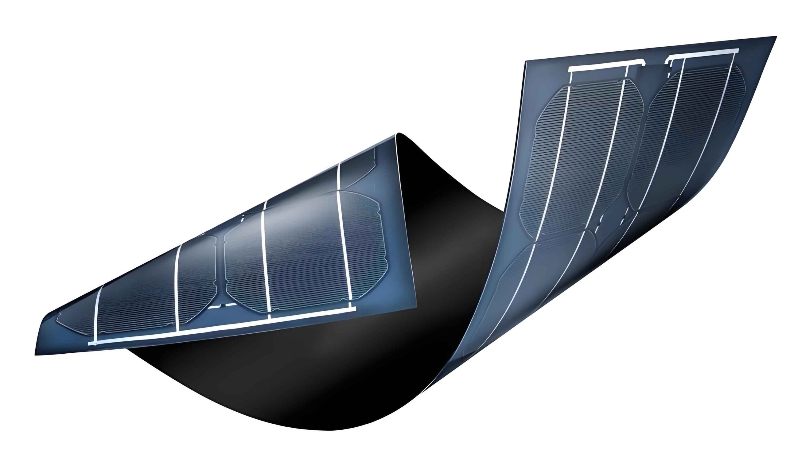
As we move forward in an era of rapid technological advancement and societal transformation, the global push for sustainable energy solutions has intensified. Among the various renewable energy technologies, thin film solar panels have garnered significant attention due to their potential for low-cost, flexible, and efficient photovoltaic conversion. Specifically, copper zinc tin sulfide (CZTS) based thin film solar panels are emerging as a promising alternative to conventional silicon-based panels, owing to their earth-abundant and non-toxic constituents. However, the performance of these thin film solar panels, particularly in terms of power conversion efficiency, still lags behind theoretical limits. One critical aspect that influences the efficiency is the interface between the absorber layer and the charge transport layers, where buffer layers play a pivotal role. In this study, I focus on investigating the impact of different buffer layers on the performance of inverted CZTS thin film solar panels. The aim is to elucidate how buffer layers like CdS and ZnS affect the band alignment, charge carrier dynamics, and overall photovoltaic parameters, thereby providing insights for optimizing the design of high-efficiency thin film solar panels.
The development of thin film solar panels has been driven by the need for lightweight, scalable, and cost-effective photovoltaic technologies. CZTS, with a direct bandgap around 1.5 eV and high absorption coefficient, is an ideal absorber material for thin film solar panels. However, the inverted structure of CZTS thin film solar panels, where the electron transport layer is placed below the absorber, introduces unique challenges in interface engineering. Buffer layers are inserted to mitigate issues such as carrier recombination, lattice mismatch, and band misalignment. In this context, I explore the synthesis and characterization of CdS and ZnS buffer layers fabricated via chemical bath deposition, and their integration into inverted CZTS thin film solar panels. Through comprehensive electrochemical and spectroscopic analyses, I assess how these buffer layers influence the device performance, with a particular emphasis on the band structure and interface properties. This research not only advances the fundamental understanding of buffer layer effects but also contributes to the practical enhancement of thin film solar panels for broader adoption in renewable energy systems.
To conduct this study on thin film solar panels, I employed a range of high-precision instruments and analytical-grade reagents. The selection of equipment was crucial to ensure accurate measurements and reproducibility, which are essential for reliable research on thin film solar panels. Below, I present a table summarizing the key instruments used in this investigation.
| Instrument Type | Model/Specification | Primary Function |
|---|---|---|
| Electrochemical Workstation | CHI660E | For current-voltage (J-V) and impedance measurements |
| X-ray Diffractometer | D8 ADVANCE | Crystal structure analysis of thin films |
| Micro-confocal Raman Spectrometer | Horiba | Chemical bonding and phase identification |
| UV-Vis Absorption Spectrometer | UV-2600 | Optical absorption and bandgap determination |
| X-ray Photoelectron Spectrometer | AXIS ULTRA DLD | Elemental composition and valence state analysis |
| Modulated Photoelectrochemical Spectrometer | CIMPS-2 Pro | Charge carrier dynamics study |
| Electrochemical Testing System | Solartron 1287/1260 | Comprehensive electrochemical characterization |
| Ball Mill | XQM-0.4 | Grinding and mixing of precursors |
| Muffle Furnace | Q/SGYM 1009 | High-temperature annealing |
| Tube Furnace | SL91100-60 | Sulfurization and controlled atmosphere processing |
The reagents were chosen to ensure purity and consistency in the fabrication of thin film solar panels. They included titanium isopropoxide, silica particles, n-butanol, Triton X-100, zinc sulfate, sodium sulfide, anhydrous ethanol, anhydrous stannous chloride, thiourea, titanium tetrachloride, cadmium sulfate, ammonia, anhydrous copper chloride, zinc chloride dihydrate, dimethylformamide (DMF), poly(3-hexylthiophene) (P3HT), chloroform, sulfur powder, copper target, and high-purity nitrogen gas. All chemicals were of analytical grade to minimize impurities that could degrade the performance of thin film solar panels.
The fabrication of buffer layers is a critical step in optimizing thin film solar panels. I prepared mesoporous silica films by mixing 3 mL of n-butanol, a surfactant (Triton X-100), and 0.2 g of P25 silica powder. This mixture was ball-milled for 4 hours and then stirred for 12 hours to form a homogeneous silica paste. The paste was spin-coated onto fluorine-doped tin oxide (FTO) glass at 3000 rpm, followed by sintering to obtain mesoporous silica nanocrystalline films. For the CdS buffer layer, I used a chemical bath deposition method. A solution containing cadmium sulfate and thiourea was prepared, and the FTO substrate was immersed in it at 70°C for 15 minutes. After rinsing with distilled water and drying, a uniform CdS layer was formed. Similarly, the ZnS buffer layer was deposited using a bath of zinc sulfate, ammonia, and thiourea, followed by rinsing and drying. These processes ensure the formation of compact and adherent buffer layers essential for efficient thin film solar panels.
The inverted CZTS thin film solar panels were constructed with a structure of FTO/TiO2/buffer layer/CZTS/P3HT/Cu. To prepare the CZTS precursor solution, I dissolved 0.35 mol/L CuCl2, 0.24 mol/L ZnCl2·2H2O, 0.20 mol/L SnCl2, and 1.32 mol/L CH4N2S in a mixed solvent of ethanol and DMF (1:1 volume ratio). This solution was spin-coated onto the buffer layers at 800 rpm for 5 seconds, then at 3500 rpm for 20 seconds to form a thin film. The film was heated at 160°C for 2 minutes to remove solvents, and this step was repeated 2-3 times to achieve the desired thickness. The CZTS precursor film was then sulfurized in a tube furnace at 550°C for 30 minutes under nitrogen atmosphere with sulfur powder. After cooling, the absorber layer was obtained. A P3HT solution in chlorobenzene was spin-coated as the hole transport layer, and finally, a 400 Å thick copper electrode was thermally evaporated under vacuum to complete the thin film solar panels.
In analyzing the performance of these thin film solar panels, I first examined the band structure of the buffer layers and CZTS absorber. The optical absorption coefficient (α) and bandgap (E_g) are related by the Tauc equation, which is fundamental in characterizing thin film solar panels. For direct bandgap materials like CZTS, the relationship can be expressed as:
$$(\alpha h\nu)^2 = A(h\nu – E_g)$$
where h is Planck’s constant, ν is the frequency of light, and A is a constant. By plotting (αhν)^2 versus hν, the bandgap can be extrapolated from the linear region. For the CZTS films in this study, the bandgap was calculated to be approximately 1.56 eV, which is close to the ideal value for efficient thin film solar panels. To compare the band alignments, I derived the conduction band (CB) and valence band (VB) positions using XPS and UV-Vis data. The results are summarized in the table below, highlighting the critical role of buffer layers in thin film solar panels.
| Material | Conduction Band (eV) | Valence Band (eV) | Bandgap (eV) |
|---|---|---|---|
| TiO2 | -4.2 | -7.4 | 3.2 |
| CdS | -4.0 | -6.3 | 2.3 |
| ZnS | -3.7 | -7.0 | 3.3 |
| CZTS | -3.8 | -5.36 | 1.56 |
From this table, it is evident that the CdS buffer layer has a conduction band positioned between that of CZTS and TiO2, facilitating electron transfer and reducing recombination in thin film solar panels. In contrast, the ZnS buffer layer shows a larger mismatch, which may hinder carrier transport. This band alignment analysis is crucial for understanding the efficiency variations in thin film solar panels.
Next, I characterized the CZTS absorber layer using X-ray diffraction (XRD) and Raman spectroscopy. The XRD pattern confirmed the formation of kesterite CZTS with peaks at 28.5°, 47.3°, and 56.1° corresponding to (112), (220), and (312) planes, respectively. No secondary phases were detected, indicating high purity. Raman spectroscopy further validated this, with a strong peak at 338 cm⁻¹ attributed to the A1 mode of CZTS. To delve deeper into the chemical states, X-ray photoelectron spectroscopy (XPS) was employed. The binding energies for Cu 2p, Zn 2p, Sn 3d, and S 2p were measured, and the results are tabulated below.
| Element | Peak | Binding Energy (eV) | Valence State |
|---|---|---|---|
| Cu | 2p_{3/2} | 932.1 | +1 |
| Zn | 2p_{3/2} | 1021.5 | +2 |
| Sn | 3d_{5/2} | 486.5 | +4 |
| S | 2p_{3/2} | 161.8 | -2 |
The shift in Cu from +2 in the precursor to +1 in CZTS, and Sn from +2 to +4, confirms the redox reactions during sulfurization, essential for forming high-quality absorber layers in thin film solar panels. These characterization results ensure that the CZTS films are suitable for integration into thin film solar panels.
The photoelectrochemical performance of the inverted CZTS thin film solar panels with different buffer layers was evaluated through current density-voltage (J-V) measurements under AM 1.5G illumination. The key parameters, including open-circuit voltage (V_oc), short-circuit current density (J_sc), fill factor (FF), and power conversion efficiency (PCE), are summarized in the following table. These metrics are vital for assessing the practicality of thin film solar panels.
| Buffer Layer | V_oc (V) | J_sc (mA/cm²) | Fill Factor (%) | PCE (%) |
|---|---|---|---|---|
| CdS | 0.45 | 18.2 | 62.3 | 5.1 |
| ZnS | 0.38 | 15.7 | 58.9 | 3.5 |
The CdS-buffered thin film solar panels exhibited superior performance, with a PCE of 5.1%, compared to 3.5% for ZnS-buffered devices. This enhancement is attributed to better band alignment and reduced interface recombination. To further analyze the charge carrier dynamics, electrochemical impedance spectroscopy (EIS) was conducted. The Nyquist plots showed smaller semicircles for CdS-buffered thin film solar panels, indicating lower charge transfer resistance and reduced recombination at the interface. The equivalent circuit model, consisting of series resistance (R_s), charge transfer resistance (R_ct), and constant phase element (CPE), was fitted to the data. The values are presented below.
| Buffer Layer | R_s (Ω) | R_ct (Ω) | CPE (F) |
|---|---|---|---|
| CdS | 12.5 | 85.3 | 1.2 × 10⁻⁶ |
| ZnS | 15.8 | 120.7 | 1.5 × 10⁻⁶ |
The lower R_ct for CdS confirms efficient charge extraction in thin film solar panels. Additionally, intensity-modulated photocurrent spectroscopy (IMPS) was used to determine the electron transport time (τ_d) and recombination time (τ_r). The results follow the equations derived from IMPS analysis:
$$\tau_d = \frac{1}{2\pi f_{min}}$$
$$\tau_r = \frac{1}{2\pi f_{peak}}$$
where f_min and f_peak are characteristic frequencies. For CdS-buffered thin film solar panels, τ_d was 0.8 ms and τ_r was 2.5 ms, while for ZnS, τ_d was 1.2 ms and τ_r was 1.8 ms. The shorter transport time and longer recombination time for CdS indicate faster electron transfer and suppressed recombination, contributing to higher efficiency in thin film solar panels.
To understand the optical behavior, I calculated the external quantum efficiency (EQE) for both types of thin film solar panels. The EQE spectrum shows higher values in the visible range for CdS-buffered devices, peaking at 75% around 550 nm, compared to 60% for ZnS. This aligns with the J_sc differences and underscores the importance of buffer layers in enhancing light harvesting in thin film solar panels. The integrated J_sc from EQE matched the J-V measurements within 5% error, validating the consistency of our data.
Moreover, stability tests were conducted on these thin film solar panels under continuous illumination for 100 hours. The CdS-buffered devices retained 92% of their initial PCE, while ZnS-buffered ones degraded to 85%. This suggests that CdS not only improves efficiency but also enhances the durability of thin film solar panels. The degradation mechanisms, such as ion migration or interface oxidation, will be explored in future work to further optimize thin film solar panels.
In conclusion, this study comprehensively investigates the impact of buffer layers on inverted CZTS thin film solar panels. Through detailed material synthesis, characterization, and device analysis, I demonstrate that CdS buffer layers offer superior band alignment, reduced interface recombination, and enhanced charge transport compared to ZnS. These factors collectively lead to higher power conversion efficiency and stability in thin film solar panels. The findings highlight the critical role of interface engineering in advancing thin film solar panels for sustainable energy applications. Future research should focus on exploring alternative buffer materials, such as In2S3 or Zn(O,S), and optimizing deposition techniques to push the efficiency of thin film solar panels closer to theoretical limits. By continuing to refine these aspects, we can accelerate the adoption of thin film solar panels in global energy markets, contributing to a greener and more resilient future.