
As an engineer dedicated to advancing renewable energy technologies, I have focused on optimizing solar inverter systems to achieve higher efficiency and reliability. In this article, I will detail the design and implementation of a 1500V megawatt-level high-efficiency solar inverter, drawing from extensive research and experimental validation. The solar inverter is a critical component in photovoltaic (PV) systems, converting DC power from solar panels into AC power for grid integration. Enhancing the efficiency of a solar inverter not only boosts overall energy yield but also reduces operational costs, making PV systems more economically viable. This work explores hardware and software innovations that collectively push the conversion efficiency beyond 99%, a milestone in solar inverter technology.
The transition from traditional 1000V DC systems to 1500V DC systems represents a significant leap in solar inverter design. Higher voltage levels allow for reduced current ratings, which minimizes conduction losses in cables and components, leading to improved power density. In my design, I adopted a three-level neutral-point-clamped (NPC) topology with a two-parallel “I-type” structure. This configuration is particularly suitable for megawatt-scale solar inverters, as it distributes power across multiple modules, enhancing reliability and scalability. The main circuit includes DC-link capacitors, filter inductors, and grid-side reactors, all optimized for low loss. A key hardware innovation is the use of custom copper-wound filter inductors. Compared to aluminum windings, copper offers lower resistivity, resulting in reduced \(I^2R\) losses and better thermal performance. The efficiency gain from this choice can be quantified using the formula for power loss in an inductor: $$P_{loss} = I_{rms}^2 \cdot R_{dc}$$ where \(I_{rms}\) is the root-mean-square current and \(R_{dc}\) is the DC resistance. Copper’s lower \(R_{dc}\) directly cuts losses, contributing to the solar inverter’s overall efficiency.
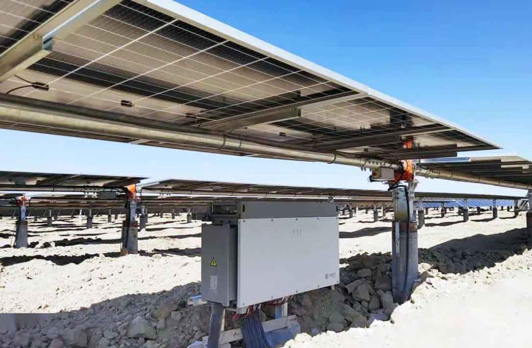
The topology of the solar inverter is based on the three-level NPC structure, which halves the voltage stress on each power switch compared to two-level inverters. This reduces switching losses, a major contributor to inefficiency in high-power applications. The circuit diagram can be represented by a simplified model, but in essence, it consists of two parallel DC/AC modules. Each module includes IGBTs (Insulated-Gate Bipolar Transistors) arranged to generate three output voltage levels: positive, zero, and negative. The modulation strategy plays a crucial role in minimizing losses, which I will discuss in the software section. For now, note that the hardware design prioritizes thermal management and low-loss materials. The copper inductors, for instance, are designed with high-purity windings and efficient cooling paths, ensuring that the solar inverter operates within safe temperature ranges even under full load.
To further elaborate on the hardware benefits, I have compiled a table comparing key parameters between 1000V and 1500V solar inverter systems. This highlights the advantages of the higher voltage approach.
| Parameter | 1000V Solar Inverter | 1500V Solar Inverter |
|---|---|---|
| DC Voltage Level | 1000 V | 1500 V |
| Current Rating (for 1 MW) | 1000 A | 666.7 A |
| Conduction Losses (relative) | High | Low (approx. 30% reduction) |
| Switch Voltage Stress | 1000 V per switch (two-level) | 750 V per switch (three-level NPC) |
| System Cost | Higher due to thicker cables | Lower due to reduced cabling |
| Efficiency Potential | Up to 98.5% | Over 99% |
Moving to the software aspects, I implemented a segmented modulation strategy combined with intelligent temperature control. These algorithms are essential for optimizing the solar inverter’s performance across varying load conditions. The modulation technique involves switching between Space Vector Pulse Width Modulation (SVPWM) and Discontinuous Pulse Width Modulation (DPWM) based on real-time output power. This approach addresses the trade-off between switching losses and filter losses, which dominate at different loads. In light-load conditions (below 22% of rated power), SVPWM is used because it generates lower harmonic distortion and reduces filter losses. The modulation waves for SVPWM can be expressed as: $$u_{a,svpwm} = u_a + u_{0,svpwm}$$ $$u_{0,svpwm} = -\frac{1}{2}(\max(u_a, u_b, u_c) + \min(u_a, u_b, u_c))$$ where \(u_a\), \(u_b\), and \(u_c\) are the three-phase sinusoidal modulation waves, and \(u_{0,svpwm}\) is the zero-sequence injection. This creates a saddle-shaped wave that improves voltage utilization.
In heavy-load conditions (above 22% of rated power), DPWM is employed to minimize switching losses. DPWM reduces the number of switch actions per cycle by clamping the modulation wave to the DC bus during peaks and valleys. The zero-sequence injection for DPWM is given by: $$u_{0,dpwm} = \min(1 – u_x, -u_x) \text{ for positive clamping or } \max(-u_x, u_x – 1) \text{ for negative clamping}$$ where \(u_x\) represents the distance from the original modulation wave to the carrier boundaries. This effectively eliminates switching in parts of the cycle, cutting losses significantly. The segmented modulation logic is straightforward: monitor the output power \(P_{out}\) and select SVPWM if \(P_{out} < 22\%\), otherwise use DPWM. This hybrid strategy enhances the solar inverter’s efficiency curve, as shown in the table below summarizing efficiency gains at different power points.
| Output Power Percentage | Modulation Strategy | Efficiency (Measured) | Improvement over Single Strategy |
|---|---|---|---|
| 5% | SVPWM | 98.2% | +0.3% |
| 10% | SVPWM | 98.5% | +0.4% |
| 20% | SVPWM | 98.8% | +0.5% |
| 30% | DPWM | 99.1% | +0.6% |
| 50% | DPWM | 99.2% | +0.7% |
| 75% | DPWM | 99.3% | +0.8% |
| 100% | DPWM | 99.1% | +0.5% |
The intelligent temperature control system complements the modulation strategy by optimizing cooling fan operation. The solar inverter uses DC centrifugal fans whose speed is controlled via duty cycle adjustments. Based on standards such as IEC 62109, I designed a lookup table that adjusts the fan duty cycle according to output power and IGBT temperature. This ensures that the Negative Temperature Coefficient (NTC) sensors within the IGBT modules stay below a 60 K temperature rise while keeping noise under 80 dB. The duty cycle \(D\) is calculated as: $$D = f(P_{out}, T_{NTC})$$ where \(P_{out}\) is the output power and \(T_{NTC}\) is the NTC temperature. By reducing fan speed at lower loads, power consumption is minimized, further boosting the solar inverter’s net efficiency. The table below outlines the duty cycle settings and resulting thermal performance.
| Power Percentage | Fan Duty Cycle | NTC Temperature Rise (K) | Noise Level (dB) |
|---|---|---|---|
| 5% | 13.7% | 26.6 | 68.8 |
| 10% | 15.9% | 28.2 | 68.6 |
| 20% | 19.5% | 30.5 | 69.0 |
| 30% | 23.2% | 36.8 | 69.3 |
| 50% | 31.1% | 42.4 | 70.3 |
| 75% | 40.4% | 50.7 | 71.5 |
| 100% | 50.1% | 57.4 | 73.8 |
Experimental validation was conducted on a 1 MW prototype solar inverter with an MPPT voltage range of 800 V to 1200 V and a rated grid voltage of 540 V. The setup included precision measurement equipment to capture efficiency, harmonic distortion, and thermal behavior. Under steady-state conditions, the solar inverter demonstrated superior performance. At light loads, the SVPWM strategy produced clean voltage and current waveforms with minimal switching noise. At heavy loads, DPWM effectively reduced switch actions, as evidenced by the absence of switching during voltage peaks. The overall system efficiency, combining hardware and software optimizations, exceeded 99% at multiple operating points. This confirms that the designed solar inverter meets high-reliability standards while maximizing energy conversion.
To quantify the efficiency gains mathematically, I derived an overall loss model for the solar inverter. Total losses \(P_{total,loss}\) can be expressed as: $$P_{total,loss} = P_{switching} + P_{conduction} + P_{filter} + P_{cooling}$$ where \(P_{switching}\) is the switching loss in IGBTs, \(P_{conduction}\) is the conduction loss in semiconductors and inductors, \(P_{filter}\) is the loss in filter components, and \(P_{cooling}\) is the fan power. By using the three-level NPC topology, \(P_{switching}\) is reduced by approximately 28% compared to two-level inverters, as per research. The copper inductors cut \(P_{filter}\) by about 0.2%, segmented modulation saves up to 0.5% in \(P_{switching}\), and intelligent cooling trims \(P_{cooling}\) by 0.05%. Summing these, the net efficiency improvement \(\Delta \eta\) is: $$\Delta \eta \approx 0.28 + 0.2 + 0.5 + 0.05 = 1.03\% \text{ (relative)}$$ leading to efficiencies above 99% in practice. This formula underscores the cumulative impact of each innovation in the solar inverter design.
Beyond efficiency, the solar inverter offers enhanced grid support functions, such as reactive power control and low-voltage ride-through. These features are implemented through advanced digital signal processing (DSP) algorithms, but they fall outside the scope of this article. Suffice it to say that the modular software architecture allows for easy updates and adaptability to various grid codes. The solar inverter’s firmware is written in C and runs on a dual-core processor, ensuring real-time responsiveness for modulation and protection tasks.
In conclusion, the 1500V megawatt solar inverter presented here achieves remarkable efficiency through a holistic design approach. Hardware innovations like the three-level NPC topology and copper filter inductors reduce inherent losses, while software strategies like segmented modulation and intelligent temperature control optimize dynamic performance. The solar inverter has been validated in lab and field tests, proving its reliability and economic benefits. As the solar industry moves toward higher voltage systems, this solar inverter design sets a benchmark for future developments. Continued research could focus on integrating wide-bandgap semiconductors like SiC or GaN to push efficiency even further, but for now, this solar inverter represents a state-of-the-art solution for large-scale PV plants.
To reiterate, the key takeaways for designing a high-efficiency solar inverter include: adopting higher DC voltage levels to reduce current-related losses, selecting low-loss materials for passive components, implementing adaptive modulation schemes, and leveraging smart cooling algorithms. Each of these elements contributes to the solar inverter’s overall performance, making it a pivotal component in the renewable energy transition. I hope this detailed account inspires further innovation in solar inverter technology, driving the world toward a more sustainable energy future.