
Organic-inorganic metal halide perovskite solar cells have emerged as leading candidates for next-generation photovoltaics due to their exceptional power conversion efficiencies, tunable bandgaps, and cost-effective fabrication processes. Among various device architectures, n-i-p structured perovskite solar cells employing tin oxide (SnO2) as the electron transport layer have demonstrated remarkable progress, with certified efficiencies reaching up to 26.21% in single-junction configurations. The SnO2 layer serves as the foundational substrate for perovskite film growth, directly influencing crystallization kinetics, interfacial quality, and ultimately, the performance of perovskite solar cells. However, the significant mismatch in thermal expansion coefficients between SnO2 and perovskite materials induces substantial residual tensile strain during thermal annealing, leading to lattice distortions, increased defect densities, and compromised operational stability. This interfacial strain represents a critical challenge in advancing perovskite solar cell technology toward commercial viability.
To address this issue, we implemented a novel interface engineering strategy incorporating two-dimensional NbSe2 nanosheets at the SnO2/perovskite buried interface. The selection of NbSe2 was motivated by its unique combination of properties: high intrinsic electrical conductivity, solution processability, absence of surface dangling bonds, and appropriate energy level alignment with adjacent layers. These characteristics make NbSe2 particularly suitable for mitigating interfacial strain while facilitating efficient charge extraction in perovskite solar cells. The NbSe2 nanosheets were synthesized through chemical lithium intercalation followed by exfoliation in aqueous medium, yielding stable dispersions of few-layer nanosheets with thicknesses approximately 25 nm and lateral dimensions below 400 nm.
Comprehensive materials characterization confirmed the structural and electronic properties of the synthesized NbSe2 nanosheets. Raman spectroscopy revealed characteristic peaks at 226 cm⁻¹ (A1g mode) and 252 cm⁻¹ (E1 2g mode), consistent with successful exfoliation while maintaining crystalline integrity. UV-visible absorption spectroscopy determined an optical bandgap of approximately 1.66 eV, in agreement with literature values for few-layer NbSe2. High-resolution transmission electron microscopy confirmed the crystalline structure with lattice fringes corresponding to the (100) plane spacing of 0.29 nm. Energy-dispersive X-ray spectroscopy mapping demonstrated uniform distribution of niobium and selenium elements throughout the nanosheets.
The integration of NbSe2 nanosheets into perovskite solar cells was systematically investigated through multiple characterization techniques. Kelvin probe force microscopy measurements revealed a significant increase in contact potential difference from 62 mV for bare SnO2 to 254 mV for SnO2/NbSe2 films, indicating reduced work function that facilitates electron extraction. X-ray photoelectron spectroscopy analysis demonstrated binding energy shifts for Sn 3d, Pb 4f, and I 3d core levels upon NbSe2 incorporation, suggesting modified interfacial interactions between SnO2 and perovskite layers. Specifically, the Sn 3d5/2 peak shifted from 486.98 eV to 486.46 eV, while Pb 4f7/2 and I 3d5/2 peaks shifted from 143.48 eV to 142.86 eV and from 619.28 eV to 618.56 eV, respectively, indicating weakened interfacial bonding that potentially allows more relaxed perovskite crystal growth.
Morphological analysis of perovskite films deposited on modified substrates showed substantial improvements in crystalline quality. Scanning electron microscopy revealed that perovskite films grown on SnO2/NbSe2 substrates exhibited larger grain sizes (approximately 1 μm) compared to those on bare SnO2 (approximately 0.77 μm), with more vertically aligned crystal orientation. X-ray diffraction patterns demonstrated enhanced intensity ratios for (100)/(110) planes, increasing from 8.22 to 13.48 after NbSe2 modification, indicating preferential orientation along the photovoltaically favorable (100) direction. This improved crystallinity is attributed to the reduced nucleation sites on the dangling bond-free NbSe2 surface and the strain-buffering effect.
Critical insight into strain relaxation was obtained through grazing-incidence X-ray diffraction analysis using the 2θ–sin²Ψ method. The (012) diffraction peak of perovskite films on SnO2/NbSe2 substrates showed significantly reduced 2θ shift variation with increasing Ψ angle compared to control samples, indicating substantial mitigation of residual tensile strain. Quantitative analysis yielded residual strain values of 20.4 MPa for NbSe2-modified interfaces versus 32.1 MPa for conventional interfaces, representing a 36% reduction. The strain relaxation mechanism can be described by the relationship between interfacial stress and material properties:
$$ \sigma = E \cdot \epsilon $$
where σ represents stress, E is Young’s modulus, and ε denotes strain. The incorporation of NbSe2 nanosheets effectively decouples the SnO2 and perovskite layers, reducing the strain transfer across the interface and minimizing lattice distortion in the perovskite absorber layer.
Steady-state and time-resolved photoluminescence spectroscopy provided compelling evidence for improved charge extraction in NbSe2-modified perovskite solar cells. The photoluminescence intensity decreased dramatically upon NbSe2 incorporation, indicating enhanced electron transfer from perovskite to the electron transport layer. Time-resolved measurements yielded average carrier lifetimes (τave) of 0.88 μs for SnO2/NbSe2/perovskite compared to 1.32 μs for SnO2/perovskite structures, with corresponding τ1 and τ2 values of 0.21 μs and 1.02 μs versus 0.36 μs and 1.40 μs, respectively. These results demonstrate accelerated charge extraction and reduced non-radiative recombination in devices with NbSe2 interlayers. The carrier dynamics can be modeled using the following rate equation:
$$ \frac{dn}{dt} = G – k_1 n – k_2 n^2 $$
where n represents carrier density, G is the generation rate, k1 denotes monomolecular (non-radiative) recombination coefficient, and k2 represents bimolecular (radiative) recombination coefficient. The reduced carrier lifetime in NbSe2-modified devices corresponds to increased extraction efficiency, contributing to improved photovoltaic performance.
Electrical characterization further confirmed the benefits of NbSe2 incorporation. Current-density measurements of ITO/SnO2/Ag and ITO/SnO2/NbSe2/Ag structures revealed enhanced conductivity in NbSe2-modified devices, attributed to the high intrinsic conductivity of the two-dimensional material. Space-charge-limited-current measurements demonstrated reduced trap state densities in both electron-only devices (from 5.9 × 10¹⁵ cm⁻³ to 4.42 × 10¹⁵ cm⁻³) and perovskite-containing devices (from 3.39 × 10¹⁶ cm⁻³ to 5.9 × 10¹⁵ cm⁻³) with NbSe2 modification. The trap density calculation follows the relationship:
$$ N_t = \frac{2\epsilon\epsilon_0 V_{TFL}}{eL^2} $$
where ε is the relative dielectric constant of perovskite (approximately 32), ε0 represents vacuum permittivity, V_TFL denotes trap-filling limit voltage, e is elementary charge, and L is the film thickness. The significant reduction in trap density directly correlates with the observed strain relaxation and improved crystalline quality in perovskite films.
| Device Configuration | PCE (%) | JSC (mA·cm⁻²) | VOC (V) | FF (%) | Trap Density (cm⁻³) |
|---|---|---|---|---|---|
| SnO2/Perovskite | 21.81 | 24.71 | 1.14 | 77.41 | 3.39 × 10¹⁶ |
| SnO2/NbSe2/Perovskite | 24.05 | 25.55 | 1.15 | 82.11 | 5.9 × 10¹⁵ |
Photovoltaic performance evaluation demonstrated remarkable improvements in devices incorporating NbSe2 nanosheets. Champion perovskite solar cells achieved power conversion efficiencies of 24.05% with short-circuit current density of 25.55 mA·cm⁻², open-circuit voltage of 1.15 V, and fill factor of 82.11%, compared to 21.81%, 24.71 mA·cm⁻², 1.14 V, and 77.41% for control devices. External quantum efficiency measurements showed enhanced spectral response across the visible spectrum, with integrated current densities of 25.27 mA·cm⁻² and 24.44 mA·cm⁻² for modified and control devices, respectively, consistent with J-V measurements. Steady-state power output at maximum power point confirmed PCEs of 22.89% and 20.40% for NbSe2-modified and control perovskite solar cells, respectively, demonstrating operational stability.
Electrochemical impedance spectroscopy analysis provided further insight into the charge transport and recombination dynamics. Nyquist plots revealed reduced charge transport resistance (Rtr) from 7.14 × 10⁴ Ω to 6.49 × 10⁴ Ω and increased recombination resistance (Rrec) from 7.33 × 10⁵ Ω to 9.42 × 10⁵ Ω with NbSe2 modification. The equivalent circuit model for impedance analysis includes series resistance (Rs), charge transport resistance (Rtr), and recombination resistance (Rrec), with corresponding constant phase elements accounting for non-ideal capacitive behavior. The improved charge transport and suppressed recombination correlate directly with the enhanced fill factor and open-circuit voltage observed in J-V characteristics.
The voltage dependence on light intensity provided additional evidence for reduced trap-assisted recombination in NbSe2-modified perovskite solar cells. The slope of VOC versus natural logarithm of light intensity decreased from 1.31 kT·q⁻¹ to 1.16 kT·q⁻¹ after NbSe2 incorporation, indicating suppressed Shockley-Read-Hall recombination. The relationship between open-circuit voltage and light intensity follows:
$$ V_{OC} = \frac{nkT}{q} \ln\left(\frac{J_{SC}}{J_0} + 1\right) $$
where n represents the ideality factor, k is Boltzmann’s constant, T is temperature, q is elementary charge, J_SC is short-circuit current density, and J_0 is reverse saturation current density. The reduced slope corresponds to a lower ideality factor, confirming diminished trap-mediated recombination pathways in the optimized perovskite solar cells.
Long-term stability assessment revealed exceptional performance retention in NbSe2-modified perovskite solar cells. Unencapsulated devices maintained over 91% of their initial efficiency after 1000 hours of storage under ambient conditions (25°C, 20-30% relative humidity), while control devices degraded completely. This enhanced stability originates from the combined effects of strain relaxation, reduced defect density, and improved interfacial adhesion in the perovskite solar cell architecture. The stability enhancement can be quantified using the degradation rate constant:
$$ \frac{PCE(t)}{PCE(0)} = e^{-kt} $$
where k represents the degradation rate constant. The significantly lower k value for NbSe2-modified perovskite solar cells demonstrates their superior operational stability compared to conventional devices.
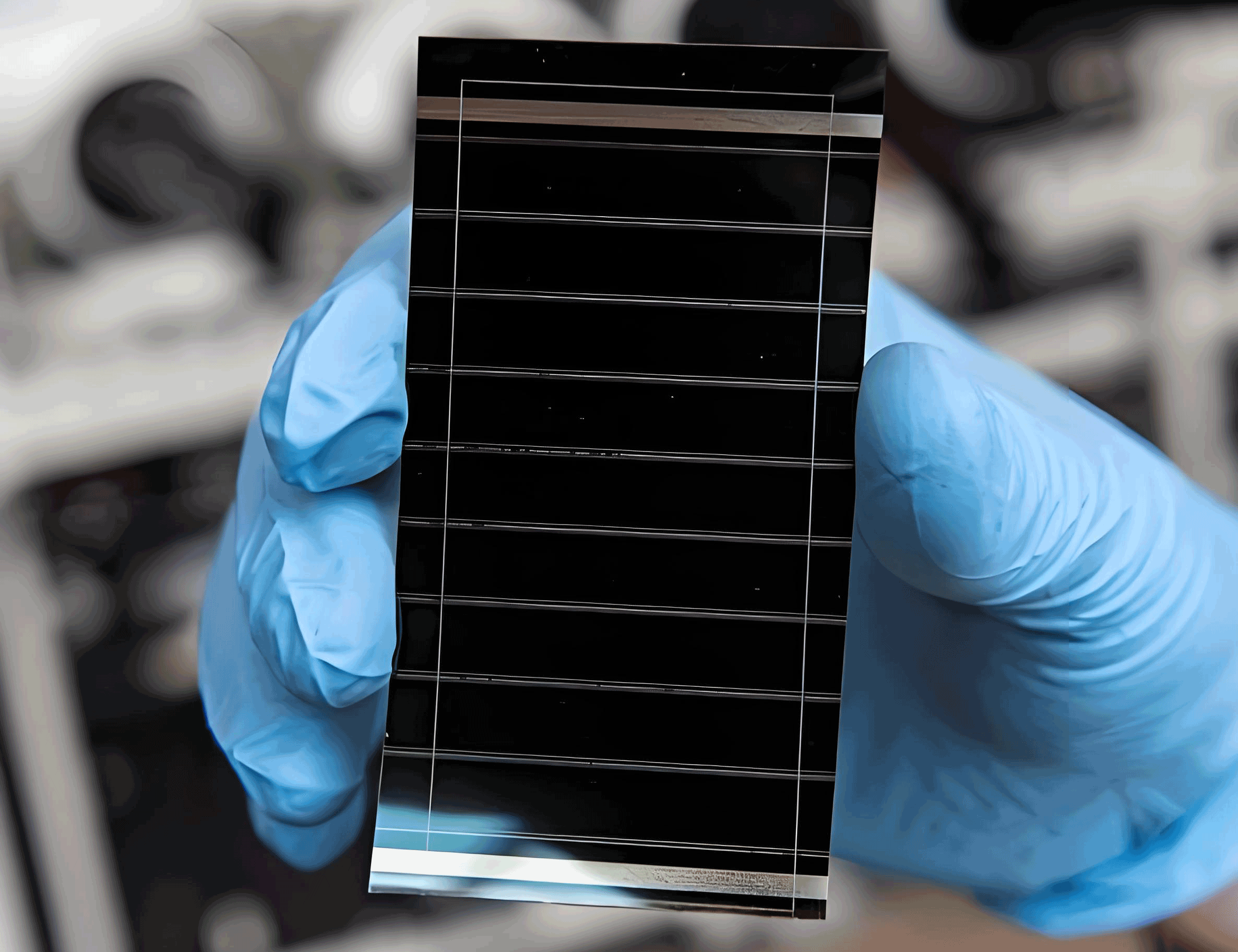
To validate the scalability of our approach, we fabricated perovskite solar minimodules with an active area of 10.12 cm² (5 cm × 5 cm) consisting of six series-connected subcells. The minimodules achieved champion efficiency of 19.54% with open-circuit voltage of 6.64 V, short-circuit current of 40.23 mA, and fill factor of 73.16%. This successful scaling demonstrates the practical viability of NbSe2 interface engineering for large-area perovskite solar cell manufacturing. The performance parameters of series-connected modules can be described by:
$$ V_{OC,module} = N \cdot V_{OC,cell} $$
$$ J_{SC,module} = J_{SC,cell} $$
$$ FF_{module} = FF_{cell} \cdot (1 – R_s G) $$
where N represents the number of series-connected cells, R_s denotes series resistance, and G is conductance. The minimal performance loss upon scaling confirms the uniform interfacial modification achieved through NbSe2 nanosheet incorporation.
| Modification Material | PCE Improvement | Strain Reduction | Trap Passivation | Stability Enhancement |
|---|---|---|---|---|
| Polymers (e.g., PS) | Moderate | Yes | Limited | Moderate |
| Small Molecules (e.g., KPF6) | Moderate | Partial | Yes | Moderate |
| 2D Materials (WS2) | Significant | Yes | Yes | Significant |
| NbSe2 Nanosheets | Exceptional | Exceptional | Exceptional | Exceptional |
In conclusion, our work demonstrates that two-dimensional NbSe2 nanosheets effectively address multiple challenges in perovskite solar cell technology through simultaneous strain relaxation, defect passivation, and optimized energy level alignment. The dangling bond-free surface of NbSe2 enables relaxed perovskite crystal growth, while its high electrical conductivity facilitates efficient charge extraction. This multi-functional interface engineering approach results in significant improvements in power conversion efficiency, operational stability, and scalability of perovskite solar cells. The fundamental insights and practical strategies presented here provide a promising pathway for developing high-performance, commercially viable perovskite photovoltaics. Future work will focus on optimizing NbSe2 nanosheet dimensions, exploring other two-dimensional materials with similar properties, and implementing this approach in tandem perovskite solar cell architectures to push beyond single-junction efficiency limits.