
In this review, I systematically analyze the recent progress in electron transport layers (ETLs) and interface engineering for perovskite solar cells (PSCs). As the global demand for clean energy continues to rise, perovskite solar cells have emerged as one of the most promising third-generation photovoltaic technologies because of their outstanding optoelectronic properties, low-cost solution processability, and rapidly increasing power conversion efficiency (PCE). Since their first report, the PCE of perovskite solar cells has surged from 3.8% to over 27%, approaching the performance of established silicon photovoltaics. However, despite these impressive gains, the practical deployment of perovskite solar cells is still constrained by several factors, including non-radiative recombination losses, imperfect energy-level alignment, and long-term operational instability. The electron transport layer plays a central role in extracting photogenerated electrons from the perovskite absorber, blocking hole backflow, and governing interfacial charge transfer. Therefore, the design and optimization of ETLs are critical for further improving both the efficiency and stability of perovskite solar cells. In the following sections, I discuss the fundamental architecture of perovskite solar cells, the main classes of ETL materials, and the multidimensional optimization strategies that have been developed to overcome existing limitations.
1. Introduction
Perovskite solar cells are based on metal halide perovskites with the general formula ABX3, where A is typically an organic cation such as methylammonium (MA+) or formamidinium (FA+), or an inorganic cation such as Cs+; B is a divalent metal cation such as Pb2+ or Sn2+; and X is a halide anion such as Cl−, Br−, or I−. This crystal structure endows perovskite materials with excellent light absorption, high carrier mobility, long diffusion lengths, and tunable bandgaps. These features make perovskite solar cells highly attractive for photovoltaic applications. The power conversion efficiency of a solar cell is generally expressed as
$$ \eta = \frac{V_{OC} J_{SC} FF}{P_{in}} $$
where \(V_{OC}\) is the open-circuit voltage, \(J_{SC}\) is the short-circuit current density, \(FF\) is the fill factor, and \(P_{in}\) is the incident power density. The fill factor is defined as
$$ FF = \frac{P_{max}}{V_{OC} J_{SC}} $$
For an ideal solar cell under illumination, the current density–voltage characteristics can be described by the diode equation
$$ J = J_0 \left( \exp\left(\frac{qV}{nkT}\right) – 1 \right) – J_{ph} $$
where \(J_0\) is the reverse saturation current density, \(q\) is the elementary charge, \(n\) is the ideality factor, \(k\) is Boltzmann’s constant, \(T\) is the absolute temperature, and \(J_{ph}\) is the photogenerated current density. In perovskite solar cells, deviations from ideal behavior arise from trap-assisted recombination, interfacial energy barriers, and imperfect charge extraction. The electron transport layer directly influences these processes by determining how efficiently electrons are extracted and how effectively holes are blocked.
I note that the performance of perovskite solar cells is strongly dependent on the quality of the ETL and the ETL/perovskite interface. A high-quality ETL should possess high electron mobility, appropriate energy-level alignment with the perovskite absorber, good chemical stability, and low defect density. In addition, the ETL should be compatible with low-temperature processing to enable flexible and large-area devices. Over the past decade, many materials have been explored as ETLs, including inorganic metal oxides, organic small molecules, polymers, and hybrid composites. Each class of materials offers distinct advantages and disadvantages, and the optimal choice often depends on the device architecture and target application.
2. Architecture and Functional Role of ETLs in Perovskite Solar Cells
The typical perovskite solar cell adopts a sandwich-like structure composed of a transparent conductive electrode, an electron transport layer, a perovskite absorber, a hole transport layer, and a metal electrode. Depending on the stacking order of the charge transport layers, perovskite solar cells are generally classified into mesoporous and planar architectures. Planar devices can be further divided into n-i-p (regular) and p-i-n (inverted) configurations. In the n-i-p architecture, the ETL is deposited on the transparent electrode, followed by the perovskite absorber and the hole transport layer. In the p-i-n architecture, the hole transport layer is deposited first, and the ETL is placed on top of the perovskite. Each configuration imposes different requirements on the ETL, particularly regarding energy-level alignment, surface passivation, and processing compatibility.
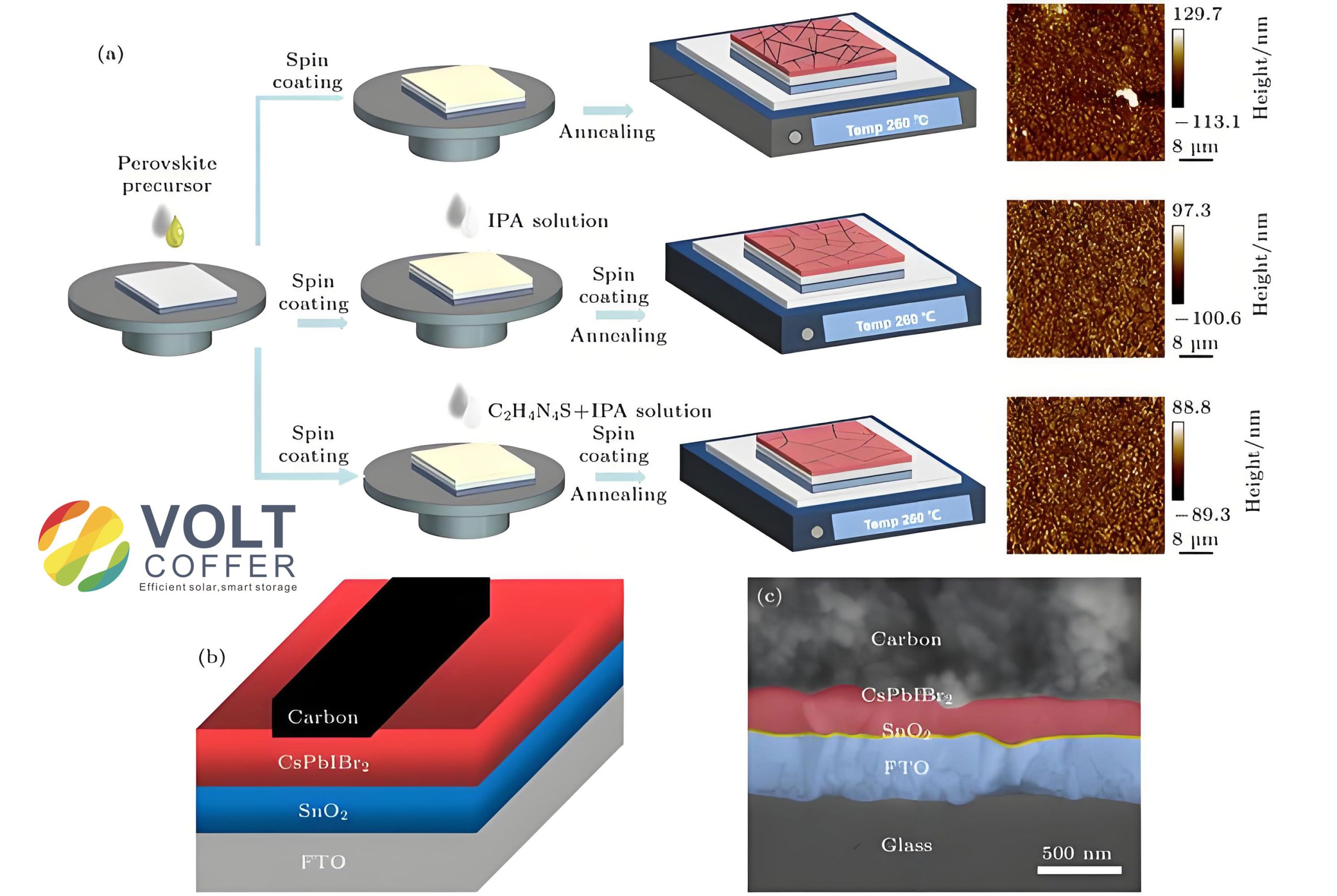
The primary function of the ETL in perovskite solar cells is to selectively extract photogenerated electrons from the perovskite layer and transport them to the external circuit while blocking holes. This selective extraction requires a favorable conduction band offset between the perovskite and the ETL. The conduction band offset is given by
$$ \Delta E_C = E_{CB}^{PVK} – E_{CB}^{ETL} $$
and the valence band offset is
$$ \Delta E_V = E_{VB}^{ETL} – E_{VB}^{PVK} $$
For efficient electron extraction, the conduction band minimum of the ETL should be close to or slightly lower than that of the perovskite, so that electrons can be injected without a significant energy barrier. Simultaneously, the valence band maximum of the ETL should be sufficiently deep to block hole injection. If the conduction band offset is too large, electrons face an extraction barrier, leading to charge accumulation and increased recombination. If the valence band offset is insufficient, holes may leak into the ETL, causing undesired recombination at the electrode.
The electron transport process in the ETL can be described by the drift-diffusion equation
$$ J_n = q n \mu_n E + q D_n \nabla n $$
where \(J_n\) is the electron current density, \(n\) is the electron density, \(\mu_n\) is the electron mobility, \(E\) is the electric field, and \(D_n\) is the electron diffusion coefficient. The diffusion coefficient is related to mobility by the Einstein relation
$$ D_n = \frac{kT}{q} \mu_n $$
The electron diffusion length in the ETL is then
$$ L_D = \sqrt{D_n \tau_n} $$
where \(\tau_n\) is the electron lifetime. A longer diffusion length means that electrons can travel farther before recombining, which is beneficial for thick ETLs and large-area devices. However, in many ETLs, trap-assisted recombination limits the effective diffusion length. The Shockley–Read–Hall recombination rate is
$$ R_{SRH} = \frac{np – n_i^2}{\tau_p (n + n_1) + \tau_n (p + p_1)} $$
where \(n_i\) is the intrinsic carrier concentration, and \(n_1\) and \(p_1\) are parameters related to trap energy levels. Reducing the density of deep-level traps in the ETL and at the ETL/perovskite interface is therefore essential for minimizing non-radiative losses.
In addition to charge extraction, the ETL also influences the crystallization of the perovskite layer. Because the perovskite film is often deposited directly onto the ETL, the surface properties of the ETL—such as roughness, wettability, and chemical composition—can affect nucleation and grain growth. A smooth and uniform ETL can promote the formation of large perovskite grains with fewer grain boundaries, thereby reducing defect density and improving charge transport. Conversely, a rough or chemically incompatible ETL can lead to poor perovskite morphology, pinholes, and increased interfacial recombination. Therefore, the ETL is not merely a passive charge transport layer but an active component that shapes the overall device performance.
3. Inorganic Electron Transport Materials
Inorganic metal oxides are among the most widely studied ETL materials for perovskite solar cells because of their high chemical stability, good electron mobility, and compatibility with established thin-film deposition techniques. The most common inorganic ETLs include titanium dioxide (TiO2), zinc oxide (ZnO), and tin dioxide (SnO2). Other materials such as Fe2O3, Nb2O5, In2O3, BaSnO3, GaN, Ti3C2Tx MXene, WO3, and CeOx have also been investigated. Each material has its own advantages and limitations, and I summarize their key parameters in Table 1.
| Material | Carrier Mobility (cm2 V−1 s−1) | Typical Device Structure | Reported PCE (%) | Key Limitations |
|---|---|---|---|---|
| TiO2 | ~0.1–10 | FTO/TiO2/MAPbI3/Spiro-OMeTAD/Au | 20.46–25.76 | Low mobility, oxygen vacancies, high annealing temperature |
| ZnO | 205–300 | FTO/ZnO/MAPbI3/Spiro-OMeTAD/Ag | 9.63–18.24 | Surface defects, moisture sensitivity, chemical instability |
| SnO2 | ~1.73–240 | FTO/SnO2/Cs0.05(FA0.83MA0.17)0.95Pb(I0.83Br0.17)3/Spiro-OMeTAD/Ag | 22.77–25.38 | Surface defects, moisture sensitivity, oxygen vacancies |
| Fe2O3 | 0.01–0.1 | FTO/Fe2O3/MAPbI3/Spiro-OMeTAD/Au | 10.78 | Low mobility, high trap density |
| Nb2O5 | 20–27 | ITO/NiOx/FA0.85MA0.15PbI2.55Br0.45/Nb2O5/Ag | 18.28 | Processing complexity, cost |
| In2O3 | ~20 | FTO/In2O3/MAPbI3/Spiro-OMeTAD/Au | 13.97 | Defect states, hysteresis |
| BaSnO3 | 70 | FTO/BaSnO3/MAPbI3/Spiro-OMeTAD/Au | 10.96 | Low efficiency, limited stability data |
| GaN | 1265 | FTO/GaN/MAPbI3/Spiro-OMeTAD/Au | 18.79 | High cost, complex fabrication |
| Ti3C2Tx | ~0.9 | ITO/Ti3C2Tx/MAPbI3/Spiro-OMeTAD/Ag | 18.29 | Oxidation sensitivity, low mobility |
| WO3 | 10–20 | FTO/WOx/(FAPbI3)1−x(MAPbBr3)x/Spiro-OMeTAD/Ag | 20.77 | Complex synthesis, high cost |
| CeOx | 100 | ITO/NiOx/MAPbI3/CeOx/Au | 17.47 | Interfacial defects, limited stability |
3.1 Titanium Dioxide (TiO2)
TiO2 is the most extensively studied inorganic ETL for perovskite solar cells. Its wide bandgap, high optical transparency in the visible region, and excellent chemical stability make it an attractive electron transport material. In mesoporous perovskite solar cells, TiO2 scaffolds provide a high surface area for perovskite infiltration and facilitate electron extraction. However, TiO2 suffers from relatively low electron mobility, which can lead to charge accumulation and increased recombination. In addition, oxygen vacancies and Ti3+ defect states are commonly formed during TiO2 deposition, creating deep-level traps that capture electrons and promote non-radiative recombination. The conduction band of TiO2 is also relatively low, which can create an energy barrier for electron injection from some perovskite compositions. Furthermore, the preparation of high-quality TiO2 often requires high-temperature sintering above 450 °C, which limits its use on flexible substrates.
To overcome these limitations, researchers have explored doping, surface modification, and nanostructuring. For example, boron doping has been shown to reduce hysteresis and improve electron extraction in TiO2-based perovskite solar cells. Niobium doping of SnO2 has also been investigated, although that belongs to the SnO2 family. For TiO2, yttrium incorporation and other metal doping strategies have been used to passivate defects and enhance conductivity. The defect density in TiO2 can be estimated from capacitance–voltage measurements using the Mott–Schottky relation
$$ \frac{1}{C^2} = \frac{2(V_{bi} – V)}{q \varepsilon N_D} $$
where \(C\) is the capacitance, \(V_{bi}\) is the built-in potential, \(\varepsilon\) is the dielectric constant, and \(N_D\) is the donor density. A higher donor density usually correlates with improved conductivity but may also indicate a higher concentration of oxygen vacancies. Therefore, an optimal balance is required.
3.2 Zinc Oxide (ZnO)
ZnO is another attractive inorganic ETL because of its high electron mobility, low cost, and low-temperature processability. Unlike TiO2, ZnO does not require high-temperature sintering, making it suitable for flexible perovskite solar cells. ZnO can be prepared in various nanostructures, including thin films, nanorods, and nanowires, which can enhance electron transport and light scattering. However, ZnO has poor chemical stability against moisture and can react with perovskite materials, leading to degradation. Surface defects such as oxygen vacancies are also common in ZnO and can act as recombination centers. To address these issues, surface passivation and doping strategies have been developed. For instance, ZrSe2 modification of ZnO has been shown to reduce surface oxygen vacancies and form interfacial dipoles that improve electron collection. Despite these advances, the long-term stability of ZnO-based perovskite solar cells remains a concern.
3.3 Tin Dioxide (SnO2)
SnO2 has emerged as a leading ETL for high-performance perovskite solar cells because of its high electron mobility, wide bandgap, good optical transparency, and excellent chemical stability. SnO2 can be processed at low temperatures, which makes it compatible with flexible substrates and roll-to-roll manufacturing. The conduction band of SnO2 is well aligned with many perovskite absorbers, facilitating efficient electron extraction. Moreover, SnO2 has a deeper valence band than TiO2, which provides better hole-blocking capability. As a result, SnO2-based perovskite solar cells have achieved PCEs exceeding 25%.
Despite these advantages, SnO2 still faces challenges related to surface defects, oxygen vacancies, and moisture sensitivity. These defects can trap electrons and promote interfacial recombination. To mitigate these issues, researchers have employed doping, surface passivation, and composite strategies. For example, hydrogen peroxide modification of SnO2 has been shown to reduce defect states and improve energy-level alignment. Niobium doping has been used to increase carrier concentration and conductivity. LiOH addition to SnO2 colloidal solutions has enabled double-layer ion diffusion doping, which improves both the ETL and the perovskite layer. The electron mobility of SnO2 is significantly higher than that of TiO2, which helps reduce charge accumulation and hysteresis.
3.4 Other Inorganic Materials
Beyond TiO2, ZnO, and SnO2, a variety of other inorganic materials have been explored as ETLs for perovskite solar cells. Fe2O3 has a suitable bandgap and good stability, but its low electron mobility limits device performance. Nb2O5 offers a high conduction band position and good electron transport, but its processing is more complex. In2O3 has been used in low-temperature processed devices, but defect states can cause hysteresis. BaSnO3 is a ternary oxide with high thermal stability, but reported efficiencies remain modest. GaN exhibits extremely high electron mobility, but its high cost and complex fabrication hinder widespread adoption. MXenes such as Ti3C2Tx have attracted attention because of their high conductivity and tunable surface chemistry, but they are prone to oxidation. WO3 has good optical transparency and can be solution-processed, but its synthesis can be challenging. CeOx has been used in inverted perovskite solar cells, but interfacial defects remain an issue.
Overall, inorganic ETLs offer excellent stability and mature processing, but they often require high-temperature annealing or suffer from interfacial defects. The choice of inorganic ETL depends on the specific device architecture and the desired trade-off between efficiency and stability.
4. Organic Electron Transport Materials
Organic electron transport materials have gained increasing attention because of their low-temperature solution processability, mechanical flexibility, and tunable electronic properties. Unlike inorganic metal oxides, organic ETLs can be chemically modified to optimize energy levels and improve compatibility with perovskite layers. Fullerene derivatives, such as [6,6]-phenyl-C61-butyric acid methyl ester (PCBM) and indene-C60 bisadduct (ICBA), are among the most widely used organic ETLs. Other organic materials include naphthalene diimide (NDI) and perylene diimide (PDI) derivatives. Table 2 summarizes key parameters of representative organic ETLs.
| Material | LUMO (eV) | Electron Mobility (cm2 V−1 s−1) | Reported PCE (%) | Stability Notes |
|---|---|---|---|---|
| PCBM | ~−4.0 | ~10−3–10−2 | Up to 18–20 | Moisture and oxygen sensitive |
| ICBA | ~−3.9 | ~10−3 | Up to 18–19 | Better stability than PCBM |
| NDI-N | ~−4.0 | ~10−3 | ~17–18 | Good film-forming properties |
| NDI-Br | ~−4.1 | ~10−3 | ~17–18 | Moderate stability |
| PDINN | ~−4.1 | ~10−3–10−2 | 17.23 (OSCs) | Good stability, low-cost synthesis |
4.1 Fullerene Derivatives
Fullerene derivatives are attractive organic ETLs because of their high electron affinity, good electron mobility, and ability to form smooth films. PCBM is the most studied fullerene derivative. Its low LUMO level of approximately −4.0 eV allows efficient electron transfer from perovskite. PCBM can also passivate surface defects on perovskite films, reducing non-radiative recombination. However, PCBM is sensitive to moisture and oxygen, which can degrade device performance over time. In addition, PCBM has weak light absorption in the visible region, which may slightly reduce photocurrent. ICBA has a slightly higher LUMO level than PCBM, which can improve open-circuit voltage. ICBA also forms better interfaces with perovskite, reducing charge recombination. Nevertheless, both PCBM and ICBA require careful encapsulation to achieve long-term stability.
4.2 NDI and PDI Derivatives
NDI and PDI derivatives are n-type organic semiconductors with excellent electron transport properties and tunable energy levels. They can be processed from solution and often exhibit good thermal stability. NDI-based ETLs, such as NDI-N and NDI-Br, have been used in perovskite solar cells with promising results. These molecules can form high-quality films and effectively extract electrons. PDI derivatives, particularly PDINN, have shown excellent performance in organic solar cells and are being explored for perovskite solar cells. PDINN contains secondary amine groups that can form hydrogen bonds with the active layer, improving interfacial contact and reducing the work function of the metal cathode. This leads to enhanced electron collection and higher fill factors. However, the electron mobility of many NDI and PDI derivatives is still lower than that of inorganic ETLs, and their long-term stability under illumination and humidity needs further improvement.
Organic ETLs offer the advantage of low-temperature processing and mechanical flexibility, but they generally suffer from lower electron mobility and poorer environmental stability compared with inorganic ETLs. Therefore, hybrid strategies that combine organic and inorganic materials are often employed to leverage the strengths of both.
5. Hybrid and Composite ETLs
Hybrid and composite ETLs aim to combine the high electron mobility and stability of inorganic materials with the tunable surface chemistry and low-temperature processability of organic materials. One example is the WO3@SnO2 nanocomposite, where WO3 is in situ peptized in an alkaline SnO2 colloid. This composite ETL provides molecular-level passivation of SnO2 defects and improves charge extraction. Devices using this ETL have achieved PCEs of 23.6% with a fill factor of 85.8%. Another example is the organic–inorganic hybrid material based on a titanium-oxo cluster and a perylene diimide derivative. This hybrid ETL combines the high electron mobility of the titanium-oxo cluster with the passivation ability of the perylene diimide. When used as an interfacial modifier between TiO2 and perovskite, it improves energy-level alignment, film morphology, and defect passivation, leading to PCEs above 20%.
Table 3 summarizes representative hybrid and composite ETLs and their performance metrics.
| Composite ETL | Key Components | Reported PCE (%) | Advantages |
|---|---|---|---|
| WO3@SnO2 | WO3 and SnO2 nanocrystals | 23.6 | High fill factor, defect passivation, improved charge extraction |
| CTOC-3-BPTI/TiO2 | Titanium-oxo cluster and perylene diimide derivative | 20.14 | Good solubility, energy-level tuning, reduced defects |
| SnO2/PCBM | SnO2 and PCBM | ~20–22 | Improved electron transport, reduced hysteresis |
| ZnO/PCBM | ZnO and PCBM | ~18–20 | Low-temperature processing, better interfacial contact |
These hybrid systems demonstrate that combining materials with complementary properties can effectively address the limitations of single-component ETLs. However, challenges related to reproducibility, large-scale manufacturing, and long-term stability remain.
6. Performance Optimization Strategies
Optimizing the ETL and the ETL/perovskite interface is essential for achieving high-efficiency and stable perovskite solar cells. I categorize the main strategies into three areas: material modification for defect control, interface engineering for improved electron injection, and structural innovation for optimized transport pathways.
6.1 Material Modification and Defect Control
Defects in ETLs can act as trap states that capture electrons and promote non-radiative recombination. These defects include oxygen vacancies, cation vacancies, antisite defects, and surface dangling bonds. Doping is a powerful approach to passivate defects and modify the electronic properties of ETLs. For example, niobium doping of SnO2 increases carrier concentration and mobility, improving electron extraction. Boron doping of TiO2 reduces hysteresis and improves device performance. Lithium doping of SnO2 through LiOH addition creates a gradient distribution of Li+ ions that improves perovskite crystallinity and device stability.
The effect of doping on defect density can be analyzed using the space-charge-limited current (SCLC) method. In the SCLC regime, the current density is
$$ J = \frac{9}{8} \varepsilon \mu \frac{V^2}{L^3} $$
where \(L\) is the film thickness. The trap-filled limit voltage \(V_{TFL}\) is related to the trap density \(N_t\) by
$$ V_{TFL} = \frac{q N_t L^2}{2 \varepsilon} $$
Therefore, a lower \(V_{TFL}\) indicates a lower trap density. Doping strategies that reduce \(V_{TFL}\) are beneficial for improving electron transport and reducing recombination.
In addition to doping, surface modification with organic molecules can passivate defects. For example, self-assembled monolayers and functional molecules containing carboxyl, hydroxyl, or amine groups can coordinate with undercoordinated metal cations on the ETL surface, reducing trap states and improving energy-level alignment. The use of 4-methoxyphenacyl potassium (MSAK) as a defect passivation agent has been shown to improve both the ETL and the perovskite layer, leading to PCEs above 25% and enhanced stability.
6.2 Interface Engineering
The ETL/perovskite interface is a critical region where charge extraction, recombination, and degradation occur. Interface engineering aims to optimize energy-level alignment, reduce defect density, and improve chemical compatibility. Common strategies include introducing buffer layers, molecular bridges, and passivation layers. For example, a multifunctional molecular bridge layer such as 2,5-dichloroterephthalic acid (DCPPA) can passivate dangling bonds and oxygen vacancies in SnO2, while also interacting with undercoordinated Pb2+ ions in the perovskite. This leads to improved electron extraction and reduced non-radiative recombination. Devices modified with DCPPA have achieved PCEs of 23.25% on small-area devices and 20.23% on larger modules.
Another approach is the use of cascade energy-level structures. By introducing a molecule with intermediate energy levels between the perovskite and the ETL, a stepped energy landscape can be created. This facilitates electron transfer and reduces the energy barrier. The cascade energy-level alignment can be described by
$$ E_{CB}^{PVK} > E_{CB}^{interlayer} > E_{CB}^{ETL} $$
Such a gradient in conduction band energy promotes directional electron flow and suppresses back transfer. In addition, the interlayer can passivate surface defects and improve perovskite crystallization. Devices with cascade energy-level structures have shown PCEs above 23% and excellent long-term stability, retaining 90% of their initial efficiency after 8000 hours of storage in ambient conditions.
Table 4 summarizes common interface engineering strategies and their effects.
| Strategy | Example Materials | Key Effects | Reported PCE (%) |
|---|---|---|---|
| Molecular passivation | MSAK, DCPPA | Defect passivation, improved energy alignment | 23.25–25.47 |
| Buffer layers | PCBM, ICBA, PDINN | Reduced recombination, improved electron extraction | 17.23–20.14 |
| Cascade energy levels | BTP-eC9, fused-ring acceptors | Dual electron transport channels, reduced carrier recombination | 23.10 |
| Self-assembled monolayers | PFPA, POAA | Energy-level tuning, chemical passivation | ~20–24 |
| Ion diffusion doping | LiOH in SnO2 | Gradient doping, improved crystallinity | ~22–24 |
6.3 Structural Innovation
Structural innovation involves designing the ETL at the micro- and nanoscale to optimize electron transport pathways and reduce defect density. Nanostructured ETLs, such as mesoporous films, nanorods, nanowires, and nanoarrays, can provide a larger interfacial area for electron extraction and shorter transport paths. For example, mesoporous SnO2 films prepared using a porogen such as polyethylene glycol (PEG) have been shown to improve carrier collection and fill factor. However, the introduction of mesopores can also create surface defects that reduce open-circuit voltage. Surface modification with RbF can passivate these defects and improve conductivity. Rb+ ions can also diffuse into the perovskite layer and suppress ion migration, enhancing stability.
Another structural innovation is the use of bubble-assisted assembly to create micro-nanostructured SnO2 arrays. These arrays serve as both the ETL and a scaffold for perovskite growth. By optimizing the electron transport path and enlarging the perovskite grain size, devices have achieved PCEs of 25.35% with certified efficiency of 25.07%. The improved performance is attributed to reduced grain boundary density and enhanced electron extraction.
The transport path length in a nanostructured ETL can be approximated by
$$ L_{eff} = \sqrt{D_n \tau_n} $$
where \(L_{eff}\) is the effective diffusion length. Nanostructures that reduce the actual distance electrons must travel to reach the electrode can increase the collection efficiency. In addition, the surface area of the ETL can be estimated as
$$ A_{eff} = A_{geo} \times R_f $$
where \(A_{geo}\) is the geometric area and \(R_f\) is the roughness factor. A higher roughness factor provides more contact area for electron transfer but may also increase defect density if not properly passivated.
Overall, structural innovation offers a promising route to improve ETL performance, but it must be carefully balanced with defect passivation and scalability. Large-scale manufacturing of nanostructured ETLs with consistent quality remains a challenge.
7. Challenges and Outlook
Despite the remarkable progress in ETL development for perovskite solar cells, several challenges remain. First, the long-term stability of perovskite solar cells is still insufficient for commercial deployment. ETLs can contribute to degradation through interfacial reactions, ion migration, and defect-induced recombination. Moisture and oxygen sensitivity of organic ETLs and some inorganic ETLs further complicates stability. Encapsulation strategies and barrier layers are essential but add cost and complexity. Second, the scalability of high-quality ETL deposition is a major hurdle. Many high-performance ETLs are prepared by spin coating, which is not suitable for large-area manufacturing. Techniques such as slot-die coating, blade coating, and spray coating need to be optimized for ETL materials. Third, the cost of some ETL materials, such as GaN and certain organic semiconductors, is high. Low-cost alternatives with comparable performance are needed.
Looking forward, I anticipate that future research will focus on several directions. One is the development of multifunctional ETLs that combine electron transport, defect passivation, and stability enhancement. For example, ETLs with built-in passivation groups or self-healing properties could improve both efficiency and lifetime. Another direction is the use of machine learning and high-throughput screening to accelerate the discovery of new ETL materials. This could help identify materials with optimal energy levels, mobility, and stability. Additionally, the integration of ETLs with tandem devices and flexible substrates will require new design rules. Low-temperature processing, mechanical robustness, and compatibility with other device layers will be critical.
From a mechanistic perspective, a deeper understanding of interfacial charge transfer and recombination is needed. Advanced characterization techniques such as transient absorption spectroscopy, impedance spectroscopy, and Kelvin probe force microscopy can provide insights into interfacial energetics and dynamics. Theoretical modeling using density functional theory and drift-diffusion simulations can guide the design of better ETLs. The combination of experimental and computational approaches will accelerate progress.
In my view, the future of perovskite solar cells depends on the successful integration of material innovation, interface engineering, and structural design. ETLs will continue to play a central role in this endeavor. By optimizing the ETL and its interface with the perovskite, researchers can push the PCE closer to the Shockley–Queisser limit while simultaneously improving stability. The Shockley–Queisser limit for a single-junction solar cell is given by
$$ \eta_{SQ} = \frac{P_{max}}{P_{in}} $$
where \(P_{max}\) is the maximum power output. For a perovskite with a bandgap of approximately 1.5 eV, the theoretical limit is around 33%. Current record efficiencies are approaching 27%, leaving room for further improvement. Reducing non-radiative recombination and improving charge extraction are key to closing this gap.
8. Conclusion
In this review, I have discussed the critical role of electron transport layers and interface engineering in perovskite solar cells. The ETL is essential for extracting photogenerated electrons, blocking holes, and stabilizing the perovskite absorber. Inorganic ETLs such as TiO2, ZnO, and SnO2 offer high stability and good electron mobility, but they suffer from surface defects, high-temperature processing, or moisture sensitivity. Organic ETLs such as fullerene derivatives and NDI/PDI-based molecules provide low-temperature processability and tunable energy levels, but their stability and electron mobility need improvement. Hybrid and composite ETLs combine the advantages of both classes and have achieved impressive efficiencies. Performance optimization strategies, including doping, interface passivation, cascade energy-level alignment, and nanostructuring, have proven effective in reducing defects and improving charge transport. Despite remaining challenges, the rapid progress in ETL design and interface engineering continues to drive the performance of perovskite solar cells toward theoretical limits. I am confident that with continued interdisciplinary research, perovskite solar cells will become a viable technology for sustainable energy generation.