
In recent years, as a renewable energy source, solar energy has garnered increasing attention, and thin film solar panels that convert light into electricity have become a focal point of research. Exploring low-cost, stable, and high-efficiency materials for thin film solar panels is currently a primary task to promote photovoltaic applications. Among various semiconductor materials, VA-VIA group metal chalcogenides (A2B3, where A = Bi, Sb and B = S, Se) have entered the research spotlight due to their promising optoelectronic properties. Antimony sulfide (Sb2S3) stands out as an excellent candidate for the active layer in novel thin film solar panels because of its superior photovoltaic characteristics.
Sb2S3 is the main component of stibnite and is an important n-type direct bandgap inorganic semiconductor material. It exhibits good photoconductive properties and thermoelectric performance, with an optical absorption coefficient greater than $5 \times 10^4 \, \text{cm}^{-1}$ in the visible region. This makes it highly suitable for thin film solar panels, where efficient light absorption is crucial. Various methods exist for preparing Sb2S3 thin films, such as chemical bath deposition, but spin-coating offers advantages like better crystallinity and purity without water introduction, minimizing oxide formation. In this study, I focus on optimizing the annealing time for Sb2S3 thin films prepared via spin-coating, as it significantly influences film crystallinity, morphology, and ultimately, the performance of thin film solar panels.
Thin film solar panels are pivotal in advancing solar technology due to their potential for lower manufacturing costs and flexibility compared to traditional silicon-based panels. The efficiency of these panels heavily depends on the quality of the light-absorbing layer. For Sb2S3-based thin film solar panels, annealing is a critical post-deposition step that enhances crystallinity and reduces defects. The annealing time can affect grain growth, film density, and optical properties, all of which impact the photovoltaic parameters. Thus, systematic investigation into annealing conditions is essential for improving the efficiency of thin film solar panels.
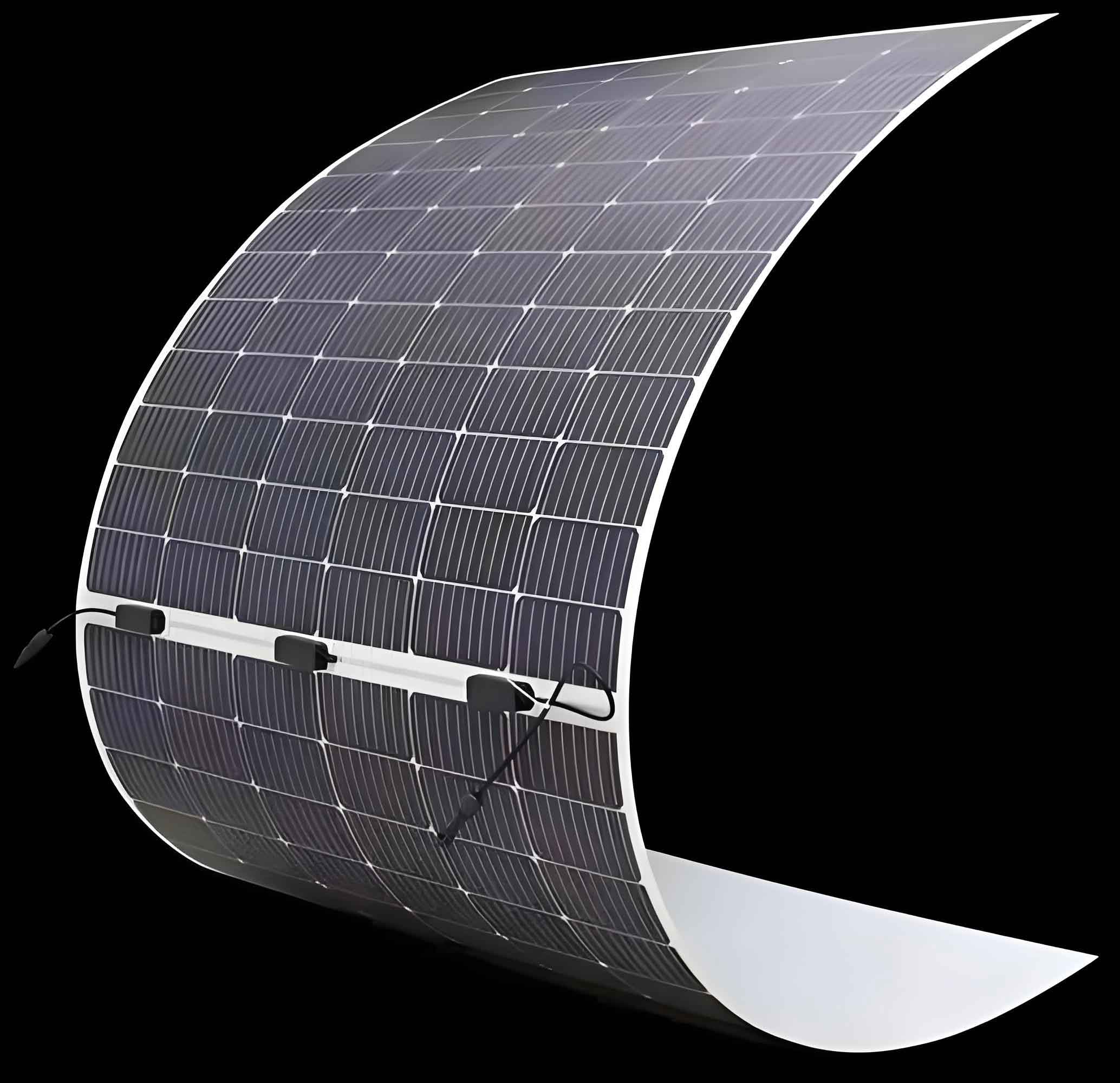
In my experimental approach, I prepared Sb2S3 thin films using a spin-coating technique. Briefly, I dissolved SbCl3 in N,N-dimethylformamide (DMF) as the antimony source, followed by the addition of thiourea (TU) to form a Sb-TU precursor solution. After stirring at room temperature for 30 minutes, I spin-coated the solution onto substrates. The samples were then transferred into a glovebox with an Ar atmosphere for annealing on a hotplate at 300°C. I varied the annealing times to 5 minutes, 10 minutes, and 15 minutes to study its effects. Subsequently, I fabricated thin film solar panels with the structure FTO/TiO2/Sb2S3/P3HT/Al, where Sb2S3 served as the light-absorbing layer. This involved depositing a TiO2 layer via sol-gel method on clean FTO, followed by the Sb2S3 layer, annealing, spin-coating a P3HT layer, and finally evaporating an Al electrode using a vacuum coater.
To characterize the films, I used X-ray diffraction (XRD) to analyze phase structure, field-emission scanning electron microscopy (SEM) to observe surface morphology, UV-Vis-NIR spectroscopy to measure optical properties, and a Keithley 4200 semiconductor parameter analyzer with a solar simulator (AM1.5) to test the current density-voltage (J-V) characteristics of the fabricated thin film solar panels. The data were then analyzed to correlate annealing time with film properties and panel performance.
The crystallinity of Sb2S3 thin films is a key factor in determining the efficiency of thin film solar panels. XRD patterns revealed significant differences based on annealing time. For films annealed for 5 minutes, the diffraction peaks were weak, and many characteristic peaks were absent, indicating incomplete crystallization due to insufficient annealing time. The crystallinity improved markedly at 10 minutes, with sharp peaks matching the standard JCPDS card (42-1393) for orthorhombic Sb2S3. No impurity phases were detected, confirming high purity. Extending annealing to 15 minutes did not further enhance crystallinity, suggesting that 10 minutes is sufficient for full crystallization. This can be summarized by the Scherrer equation for crystallite size estimation:
$$D = \frac{K \lambda}{\beta \cos \theta}$$
where $D$ is the crystallite size, $K$ is the shape factor (approximately 0.9), $\lambda$ is the X-ray wavelength, $\beta$ is the full width at half maximum (FWHM) in radians, and $\theta$ is the Bragg angle. As annealing time increases from 5 to 10 minutes, $\beta$ decreases, leading to larger $D$, but beyond 10 minutes, $\beta$ stabilizes, indicating no further grain growth. This crystallinity directly impacts the charge transport in thin film solar panels.
Surface morphology, as observed via SEM, also varied with annealing time. Films annealed for 5 minutes showed porous structures with numerous voids, which can lead to high recombination losses in thin film solar panels. At 10 minutes, the films became dense and uniform, with Sb2S3 clusters coalescing effectively, promoting better interfacial contact in the device. However, at 15 minutes, the morphology degraded, with increased porosity, likely due to over-annealing causing material evaporation or stress-induced cracking. This morphological analysis highlights the importance of optimizing annealing time for high-quality thin film solar panels. The density of the film can be related to its optical and electrical properties; a denser film typically has higher absorption and lower series resistance.
Optical absorption spectra demonstrated that films annealed for 10 minutes had the highest absorption intensity across the visible range, which is beneficial for thin film solar panels as it enhances light harvesting. The absorption coefficient $\alpha$ can be calculated from the absorbance $A$ using the formula:
$$\alpha = \frac{2.303 A}{t}$$
where $t$ is the film thickness. For a direct bandgap material like Sb2S3, the bandgap $E_g$ can be estimated from Tauc plot:
$$(\alpha h\nu)^2 = B(h\nu – E_g)$$
where $h\nu$ is the photon energy and $B$ is a constant. I observed that films annealed for 10 minutes had a bandgap around 1.7 eV, ideal for thin film solar panels, while shorter or longer annealing times led to slight variations due to changes in crystallinity and defect states. Enhanced absorption correlates with higher short-circuit current density ($J_{sc}$) in thin film solar panels.
The performance of the fabricated thin film solar panels was evaluated through J-V measurements under AM1.5 illumination. The key photovoltaic parameters—open-circuit voltage ($V_{oc}$), short-circuit current density ($J_{sc}$), fill factor (FF), and power conversion efficiency (PCE)—are summarized in Table 1 for different annealing times. The data clearly show that annealing for 10 minutes yields the best results, with a PCE of 1.91%. This optimization is critical for advancing Sb2S3-based thin film solar panels.
| Annealing Time (min) | $V_{oc}$ (V) | $J_{sc}$ (mA/cm2) | FF (%) | PCE (%) |
|---|---|---|---|---|
| 5 | 0.56 | 3.49 | 33.3 | 0.65 |
| 10 | 0.62 | 6.80 | 45.4 | 1.91 |
| 15 | 0.61 | 5.74 | 33.7 | 1.18 |
The improvement at 10 minutes can be attributed to optimal crystallinity and morphology, which reduce trap states and enhance charge collection. The $V_{oc}$ is influenced by the built-in potential and recombination, while $J_{sc}$ depends on light absorption and carrier extraction. The fill factor reflects the diode quality and series/shunt resistances. For thin film solar panels, achieving a balance between these parameters is essential, and annealing time plays a pivotal role.
To further analyze the device physics, I consider the diode equation for thin film solar panels:
$$J = J_{ph} – J_0 \left[ \exp\left(\frac{q(V + J R_s)}{n k T}\right) – 1 \right] – \frac{V + J R_s}{R_{sh}}$$
where $J_{ph}$ is the photocurrent density, $J_0$ is the reverse saturation current density, $q$ is the electron charge, $V$ is the voltage, $R_s$ is the series resistance, $n$ is the ideality factor, $k$ is Boltzmann’s constant, $T$ is temperature, and $R_{sh}$ is the shunt resistance. From the J-V curves, I extracted these parameters for different annealing times, as shown in Table 2. The lower $R_s$ and higher $R_{sh}$ for the 10-minute annealed films contribute to the better FF and PCE, underscoring the importance of annealing optimization in thin film solar panels.
| Annealing Time (min) | $J_0$ (mA/cm2) | $n$ | $R_s$ (Ω cm2) | $R_{sh}$ (Ω cm2) |
|---|---|---|---|---|
| 5 | $2.3 \times 10^{-4}$ | 2.1 | 15.6 | 320 |
| 10 | $8.7 \times 10^{-5}$ | 1.8 | 8.9 | 850 |
| 15 | $1.5 \times 10^{-4}$ | 2.0 | 12.4 | 480 |
The ideality factor $n$ close to 2 indicates dominant recombination in the depletion region, but the lower $n$ at 10 minutes suggests reduced recombination, aligning with better crystallinity. These insights are valuable for designing efficient thin film solar panels. Moreover, the stability of Sb2S3-based thin film solar panels under operational conditions is another aspect influenced by annealing. Proper annealing can improve film adhesion and reduce degradation over time, making it a key step in the fabrication process.
In terms of broader implications, the optimization of annealing time for Sb2S3 thin films contributes to the development of low-cost and scalable thin film solar panels. Compared to other materials like perovskite or CIGS, Sb2S3 offers advantages in terms of abundance and non-toxicity, which are important for sustainable energy solutions. Future work could explore tandem structures or interface engineering to further boost the efficiency of thin film solar panels beyond the 1.91% achieved here.
In conclusion, my investigation into the effect of annealing time on Sb2S3-based thin film solar panels reveals that 10 minutes at 300°C in an Ar atmosphere yields the best film crystallinity, morphology, optical absorption, and device performance. This optimization leads to a power conversion efficiency of 1.91%, demonstrating the critical role of post-deposition treatments in enhancing the viability of thin film solar panels. As research progresses, such findings will aid in the commercialization of efficient and durable thin film solar panels for global energy needs.