
In recent years, the growing demand for renewable energy has highlighted the importance of distributed power generation systems (DPGS). The on-grid inverter serves as a critical interface between renewable energy sources and the grid, injecting high-quality and stable current. To reduce grid current harmonics, L-type and LCL-type filters are widely used. Compared to the L-type filter, the LCL-type filter offers better high-frequency harmonic attenuation and requires less total inductance, leading to a smaller volume. However, the inherent resonance of the LCL filter can cause instability. To address this, damping methods are essential, which can be passive or active. Passive damping involves adding resistors to the filter topology, which is effective but incurs significant power losses. Active damping, achieved through digital filters or feedback of state variables, is lossless. Among these, capacitor-current-feedback active damping is popular due to its simplicity and effectiveness.
Most on-grid inverters are digitally controlled for high flexibility. However, digital control introduces a 1.5-sample control delay, which deteriorates the damping performance. In such cases, the capacitor-current feedback no longer acts as a virtual resistor but as a frequency-dependent virtual impedance. This introduces negative damping regions between $f_s/6$ and $f_s/2$, where $f_s$ is the sampling frequency, weakening the stability and robustness of the on-grid inverter against grid impedance variations. Specifically, when the resonance frequency $f_r$ approaches $f_s/6$, insufficient gain margin can lead to instability. Moreover, when $f_r = f_s/6$, the system becomes unstable regardless of the damping coefficient. Therefore, compensating for the control delay is crucial to enhance the robustness of the on-grid inverter.
Existing methods to mitigate the delay impact include directly reducing the delay or using control techniques like Smith predictors or state observers. However, these methods have limitations such as sensitivity to parameter variations or computational complexity. Some approaches use filters like SOGI or notch filters to expand the positive damping region to $f_s/4$, but they may not suffice for higher resonance frequencies. Others employ high-pass filters for RC or RLC damping, broadening the positive damping region to nearly $f_s/3$, but they can amplify high-frequency noise. In this work, we propose an improved delay compensation method by inserting a biquad filter into the capacitor-current feedback path. This compensates for the phase lag caused by the digital control delay, expanding the positive damping region to $f_s/3$, thereby achieving high robustness against grid impedance variations for the on-grid inverter.
We begin by analyzing the impact of digital control delay on the LCL-type on-grid inverter. The system model includes an LCL filter with inverter-side inductance $L_1$, filter capacitor $C$, and grid-side inductance $L_2$. The grid impedance is modeled as a pure inductance $L_g$ to represent the worst-case scenario. The control loop consists of a PR current controller $G_R(s)$, a digital delay $G_d(s) = e^{-1.5T_s s}$, and a capacitor-current feedback path with gain $H_{i1}$. The open-loop gain $T_D(s)$ is derived as:
$$ T_D(s) = \frac{H_{i2} K_{PWM} G_d(s) G_R(s)}{s^3 L_1 L_T C + s^2 L_T H_{i1} K_{PWM} G_d(s) G_{pl}(s) C + s(L_1 + L_T)} $$
where $L_T = L_2 + L_g$, $K_{PWM}$ is the inverter gain, and $G_{pl}(s)$ is the phase-lead compensator. The equivalent virtual impedance $Z_{eq}(s)$ introduced by capacitor-current feedback is:
$$ Z_{eq}(s) = \frac{L_1}{H_{i1} K_{PWM} C} e^{-1.5T_s s} $$
In the frequency domain, $Z_{eq}(j\omega)$ can be decomposed into a virtual resistor $R_{eq}(\omega)$ and virtual reactance $X_{eq}(\omega)$:
$$ R_{eq}(\omega) = \frac{L_1}{H_{i1} K_{PWM} C \cos(1.5\omega T_s)}, \quad X_{eq}(\omega) = \frac{L_1}{H_{i1} K_{PWM} C \sin(1.5\omega T_s)} $$
The frequency characteristics show that $R_{eq}(\omega)$ is positive for $f_r < f_s/6$ and negative for $f_s/6 < f_r < f_s/2$. Thus, $f_s/6$ is the critical frequency $f_{cri}$, defining the boundary of the positive damping region. This limits the stability of the on-grid inverter, especially under weak grid conditions where $L_g$ varies.
To compensate for the delay, we propose inserting a biquad filter $G_{pl}(s)$ in the feedback path. The biquad filter is designed in the s-domain and then discretized using the Tustin method for digital implementation. The transfer function of the biquad filter is:
$$ G_{pl}(s) = \frac{s^2 + 2\alpha\omega_\alpha s + \omega_\alpha^2}{s^2 + 2\beta\omega_\beta s + \omega_\beta^2} $$
where $\alpha$ and $\beta$ are damping ratios, and $\omega_\alpha$ and $\omega_\beta$ are natural frequencies. Based on the compensation criteria—avoiding excessive phase lead at low frequencies, maximizing phase compensation at high frequencies, and balancing magnitude gain—we set $\alpha = \beta = 0.71$, $\omega_\beta = 0.5\omega_s$ (with $\omega_s = 2\pi f_s$), and $\omega_\alpha = 0.04\omega_s$. This design expands the positive damping region to $f_s/3$.
After compensation, the equivalent impedance becomes:
$$ Z_{eq1}(j\omega) = \frac{L_1}{H_{i1} K_{PWM} C G_{pl}(e^{j\omega T_s})} e^{-1.5j\omega T_s} $$
The virtual resistor $R_{eq1}(\omega)$ after compensation is positive up to $f_s/3$, as shown in the frequency characteristics. This enhances the robustness of the on-grid inverter against grid impedance variations.
We analyze the stability of the compensated system using the Jury stability criterion. The characteristic equation in the z-domain is derived from the open-loop gain. The stability conditions are summarized in Table 1, which outlines different cases based on the resonance frequency $f_r$ and feedback coefficient $H_{i1}$.
| Case | $f_r$ Range | $H_{i1}$ Range | Stability Requirements |
|---|---|---|---|
| 1 | $0 < f_r < f_s/3$ | $0 < H_{i1} < H_{i1\_min}$ | Gain at $f_{c1}$ < 0 dB |
| 2 | $0 < f_r < f_s/3$ | $H_{i1} > H_{i1\_min}$ | Gain at $f_{c2}$ < 0 dB, Gain at $f_{c3}$ and $f_{c4}$ > 0 dB |
| 3 | $0 < f_r < f_s/3$ | $H_{i1} > H_{i1\_cri}$ | Unstable |
| 4 | $f_s/3 < f_r < f_s/2$ | $0 < H_{i1} < H_{i1\_min}$ | Gain at $f_{c2}$ < 0 dB, Gain at $f_{c3}$ and $f_{c4}$ > 0 dB |
| 5 | $f_s/3 < f_r < f_s/2$ | $H_{i1} > H_{i1\_cri}$ | Unstable |
Here, $H_{i1\_min}$ and $H_{i1\_cri}$ are critical values derived from the stability analysis. Case 1 offers the simplest stability requirement, making it desirable for the on-grid inverter design.
Next, we present a detailed closed-loop parameter design procedure to ensure good control performance. The design goals include a phase margin $PM > 45^\circ$, gain margins $GM_1 > 3$ dB and $GM_2 < -3$ dB, and a base-frequency loop gain $T_{f_0} > 73$ dB. The crossover frequency $f_c$ is set to $0.04\omega_s$. The proportional gain $K_P$ of the PR controller is calculated as:
$$ K_P \approx \frac{2\pi f_c (L_1 + L_2)}{H_{i2} K_{PWM}} $$
The resonant gain $K_r$ is constrained by the base-frequency loop gain:
$$ K_{r\_T_{f_0}} = \frac{2\pi(L_1 + L_2)(f_c^2 – f_0^2 \cdot 10^{T_{f_0}/20})}{H_{i2} K_{PWM}} $$
where $f_0$ is the grid fundamental frequency. To mitigate weak grid effects, we choose $K_r = 170$. The damping coefficient $H_{i1}$ is designed based on phase margin and gain margin constraints:
$$ H_{i1\_PM} = \frac{2\pi(f_r^2 – f_c^2)\sqrt{A^2 + B^2} \cdot G}{f_c K_{PWM}(M^2 + N^2)} $$
where $A$, $B$, $G$, $M$, and $N$ are functions of system parameters and design specifications. Similarly, $H_{i1}$ must satisfy gain margin requirements at frequencies $f_{c1}$ and $f_{c3}$:
$$ H_{i1\_GM1} = \frac{\pi L_1(f_r^2 – f_{c1}^2)\sqrt{A^2 + B^2}}{f_{c1} K_{PWM} D \sqrt{Q^2 A^2 + B^2}}, \quad H_{i1\_GM2} = \frac{L_1 K_{PWM}}{2\pi f_{c3} D} $$
After evaluating these constraints, we select $H_{i1} = 0.22$ for the on-grid inverter. The compensated system’s closed-loop poles remain inside the unit circle for grid impedance variations from 0 to 1.93 mH, confirming stability.
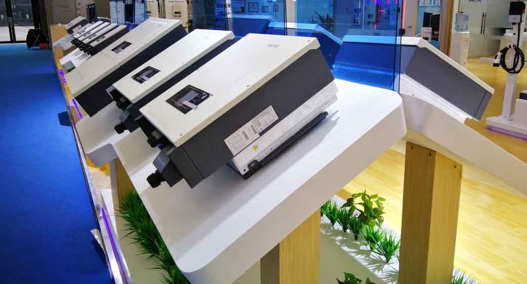
To validate the proposed method, we built a 2 kW single-phase on-grid inverter experimental prototype. The parameters are listed in Table 2.
| Parameter | Value |
|---|---|
| Input voltage $U_{dc}$ | 180 V |
| Grid voltage $U_g$ | 110 V |
| Output power $P_o$ | 2 kW |
| Inverter-side inductance $L_1$ | 800 μH |
| Filter capacitor $C$ | 5 μF |
| Grid-side inductance $L_2$ | 300 μH |
| Resonance frequency $f_r$ | 4.6 kHz |
| Sampling frequency $f_s$ | 20 kHz |
| Switching frequency $f_{sw}$ | 10 kHz |
| Grid current sampling coefficient $H_{i2}$ | 0.15 |
| Damping coefficient $H_{i1}$ | 0.22 |
| Proportional gain $K_P$ | 0.58 |
| Resonant gain $K_r$ | 170 |
The experimental results show that without compensation, the on-grid inverter becomes unstable when grid impedance $L_g$ is 0.32 mH or 1.15 mH, as the resonance frequency enters the negative damping region near $f_s/6$. With the proposed biquad filter compensation, the on-grid inverter remains stable under all tested grid impedances, with grid current THD below 2.26% even at $L_g = 1.93$ mH. Dynamic tests under half-load to full-load transitions also demonstrate stable performance, verifying the robustness of the on-grid inverter.
In conclusion, we have proposed a delay compensation method using a biquad filter for LCL-type on-grid inverters. The method effectively compensates for the phase lag caused by digital control delay, expanding the positive damping region to $f_s/3$. This enhances the stability and robustness of the on-grid inverter against grid impedance variations. A detailed parameter design procedure ensures good control performance. Experimental results from a 2 kW prototype confirm the effectiveness of the method. Future work could explore adaptive tuning of the biquad filter parameters for further optimization under varying grid conditions. Overall, this approach contributes to the reliable operation of on-grid inverters in renewable energy systems.