
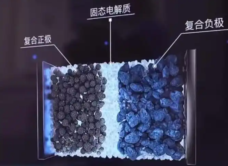
I view the solid state cell as one of the most promising pathways for reconciling high energy density with intrinsic safety in next-generation electrochemical energy storage. In a solid state cell, the liquid electrolyte and its associated flammable organic solvent network are replaced by a solid electrolyte, which can potentially suppress thermal runaway and enable high-capacity electrode materials such as lithium metal and high-nickel layered oxides. However, my analysis of solid state cell behavior consistently returns to one central bottleneck: the solid–solid interface. Unlike a liquid system, where the electrolyte can wet rough electrode surfaces and maintain intimate contact over large areas, a solid state cell relies on mechanical contact between two rigid or semi-rigid solids. This contact is discrete, heterogeneous, and dynamically evolving. The performance, rate capability, cycle life, and safety of a solid state cell are therefore not solely determined by bulk material properties but by the coupled structural, chemical, electrochemical, and mechanical behavior of interfaces.
I structure this discussion around two connected themes. First, I examine the failure mechanisms that dominate solid state cell interfaces: limited contact, interfacial reactions, space-charge-layer effects, mechanical mismatch, and their multi-factor coupling. Second, I review engineering strategies that aim to regulate these interfaces, including surface coatings, artificial interlayers, in situ interfacial adaptation, multiscale structural design, and data-driven design methods. Throughout, I emphasize that the solid state cell interface is not a static boundary but a dynamic region whose evolution determines ion transport, current distribution, and long-term stability.
The central premise I adopt is that the solid state cell interface is a multi-scale, multi-physics system. Its behavior can be summarized by a set of coupled variables: effective contact area, local current density, interfacial resistance, chemical potential gradients, stress fields, and defect distributions. A useful starting point is the definition of effective contact area:
$$A_{\text{eff}} = \int_{\Omega} \mathbf{1}_{\text{contact}}(\mathbf{r}) \, d\mathbf{r},$$
where \(\mathbf{1}_{\text{contact}}(\mathbf{r})\) is an indicator function that equals one at points where the solid electrolyte and electrode are in intimate contact and zero at voids or gaps. In an ideal liquid electrolyte system, \(A_{\text{eff}}\) approaches the geometric area \(A_{\text{geo}}\). In a solid state cell, \(A_{\text{eff}}\) is often much smaller than \(A_{\text{geo}}\) because of surface roughness, elastic modulus mismatch, and imperfect stacking pressure.
The local current density \(J_{\text{local}}\) is then related to the applied current \(I\) by:
$$J_{\text{local}}(\mathbf{r}) = \frac{I}{A_{\text{eff}}(\mathbf{r})}.$$
When \(A_{\text{eff}}\) is non-uniform, \(J_{\text{local}}\) becomes spatially concentrated. This concentration accelerates lithium deposition, promotes dendrite initiation, and drives heterogeneous interfacial reactions. I therefore treat contact loss as the first and most immediate failure mechanism in a solid state cell.
Interface Contact Limitation and Non-Uniform Local Transport
In my assessment, the most visible interfacial failure in a solid state cell is the loss of continuous contact. Solid electrolytes and electrode materials rarely form a perfect interface. Surface roughness at the micro- and nanoscale, differences in elastic modulus, and the absence of a wetting liquid phase mean that the real contact area is far below the geometric area. The interface contains pores, gaps, and microcavities. These features are not merely passive voids; they redirect ion transport, distort the electric field, and create localized hot spots of current.
I can express the ion flux in the solid electrolyte by a generalized Nernst–Planck relation:
$$\mathbf{N}_i = -D_i \nabla c_i – \frac{z_i F D_i c_i}{RT} \nabla \phi,$$
where \(\mathbf{N}_i\) is the flux of species \(i\), \(D_i\) is the diffusion coefficient, \(c_i\) is the concentration, \(z_i\) is the charge number, \(F\) is the Faraday constant, \(R\) is the gas constant, \(T\) is the temperature, and \(\phi\) is the electric potential. At a discontinuous interface, the boundary conditions for \(\mathbf{N}_i\) are not uniform. Some regions accept flux readily, while others block it. The result is a spatially modulated flux that feeds back into deposition and reaction kinetics.
During charging, lithium deposition preferentially occurs at regions of high local current density. If the current density exceeds a critical value, lithium can penetrate along grain boundaries, voids, or other defects. I define a simplified critical current density criterion:
$$J_{\text{crit}} \approx \frac{2 \gamma \Omega}{F \eta_{\text{int}} L_{\text{def}}},$$
where \(\gamma\) is the interfacial energy, \(\Omega\) is the molar volume of lithium, \(\eta_{\text{int}}\) is the interfacial overpotential, and \(L_{\text{def}}\) is a characteristic defect length. This expression is not universal, but it captures the competition between interfacial energy, driving force, and defect geometry. In a solid state cell, \(J_{\text{crit}}\) is often low because defects are abundant and contact is imperfect.
As cycling proceeds, contact degradation becomes self-reinforcing. Voids expand, effective contact area decreases, local current density increases, and lithium deposition becomes even more non-uniform. The interface evolves from a partially contacted state to a discontinuous state, and eventually a through-thickness failure path can form. Table 1 summarizes this mechanism.
| Failure Mode | Primary Variables | Intermediate Effect | Final Consequence |
|---|---|---|---|
| Contact limitation | \(A_{\text{eff}}\), roughness, modulus mismatch | Local current concentration | Dendrite initiation, capacity fade |
| Void expansion | Stress, pressure, creep | Loss of ion pathways | Impedance rise, mechanical separation |
| Non-uniform deposition | \(J_{\text{local}}\), overpotential | Filament growth | Short circuit, thermal event |
Interfacial Chemical Reactions and High-Impedance Layer Formation
My second concern is chemical and electrochemical instability. A solid state cell often pairs a solid electrolyte with an electrode that is thermodynamically incompatible with it. For example, sulfide solid electrolytes can be reduced by lithium metal, forming lithium sulfide, phosphides, and other reaction products. Oxide solid electrolytes may form lithium-rich oxide interfacial layers. Polymer solid electrolytes can undergo decomposition or cross-linking. These reactions are driven by differences in lithium chemical potential and by the applied electrochemical potential.
I describe the driving force for interfacial reaction using the change in Gibbs free energy:
$$\Delta G_{\text{int}} = \Delta G^\circ + RT \ln Q,$$
where \(Q\) is the reaction quotient. When \(\Delta G_{\text{int}} < 0\), the reaction is thermodynamically favorable. In a solid state cell, the reaction products often form a thin layer that may be ionically conductive, electronically insulating, or mixed conducting. If the layer is ionically insulating, it increases interfacial resistance. If it is electronically conductive, it can catalyze further decomposition. If it is mixed conducting, it may allow continuous reaction and thickening.
The interfacial resistance \(R_{\text{int}}\) can be decomposed into several contributions:
$$R_{\text{int}} = R_{\text{contact}} + R_{\text{reaction}} + R_{\text{space charge}} + R_{\text{transport}},$$
where \(R_{\text{contact}}\) arises from incomplete contact, \(R_{\text{reaction}}\) from the reaction layer, \(R_{\text{space charge}}\) from charge redistribution, and \(R_{\text{transport}}\) from bulk or grain-boundary limitations near the interface. As the reaction layer grows, \(R_{\text{reaction}}\) increases. As contact is lost, \(R_{\text{contact}}\) increases. The two effects couple and produce a feedback loop.
I summarize the relationship between reaction product properties and solid state cell performance in Table 2.
| Reaction Product Character | Ionic Conductivity | Electronic Conductivity | Impact on Solid State Cell |
|---|---|---|---|
| Ionically insulating | Low | Low | High impedance, blocked ion transfer |
| Electronically conductive | Variable | High | Continuous decomposition, unstable interface |
| Mixed conducting | Moderate | Moderate | Layer growth, potential-dependent stability |
| Stable ion conductor | High | Low | Passivation, reduced further reaction |
The reaction kinetics can be expressed as:
$$i_{\text{int}} = i_0 \left[ \exp\left(\frac{\alpha_a F \eta}{RT}\right) – \exp\left(-\frac{\alpha_c F \eta}{RT}\right) \right],$$
where \(i_{\text{int}}\) is the interfacial current density, \(i_0\) is the exchange current density, \(\alpha_a\) and \(\alpha_c\) are transfer coefficients, and \(\eta\) is the overpotential. When the reaction layer has low ionic conductivity, \(i_0\) decreases, and the overpotential required for a given current increases. This further distorts the local potential distribution and can accelerate side reactions elsewhere.
Space-Charge Layer Effects and Restricted Ion Migration
In a solid state cell, the interface is also an electrostatic region. When the lithium chemical potential differs between the electrode and the solid electrolyte, lithium ions and electrons redistribute near the interface. This creates a space-charge layer with a potential gradient. The Poisson equation governs the potential profile:
$$\nabla \cdot (\varepsilon \nabla \phi) = -\rho,$$
where \(\varepsilon\) is the dielectric permittivity and \(\rho\) is the net charge density. The space-charge layer changes the local ion concentration and creates an additional migration barrier. For a solid state cell with low ionic conductivity or poor interfacial matching, this barrier can dominate the total interfacial resistance.
I can approximate the space-charge potential \(\Delta \phi_{\text{sc}}\) by:
$$\Delta \phi_{\text{sc}} \approx \frac{k_B T}{e} \ln\left(\frac{c_{\text{int}}}{c_{\text{bulk}}}\right),$$
where \(c_{\text{int}}\) and \(c_{\text{bulk}}\) are the ion concentrations at the interface and in the bulk, respectively. A large concentration difference produces a large potential barrier. This barrier reduces the effective ionic conductivity near the interface and contributes to the overall impedance of the solid state cell. The space-charge layer is not independent of reaction layers; the two often overlap, making the interface a combined chemical and electrostatic bottleneck.
Table 3 summarizes the space-charge-layer effect.
| Feature | Physical Origin | Measurable Signature | Effect on Solid State Cell |
|---|---|---|---|
| Charge redistribution | Chemical potential mismatch | Potential shift | Additional migration barrier |
| Ion depletion | Space-charge field | Low interfacial conductivity | Increased impedance |
| Overlap with reaction layer | Coupled chemical-electrostatic field | Broad impedance spectra | Rate limitation, polarization |
Mechanical Mismatch and Interfacial Structural Degradation
I consider mechanical failure to be inseparable from electrochemical failure in a solid state cell. Solid electrolytes are often stiff and brittle, while electrode materials undergo significant volume changes during charge and discharge. For example, lithium metal deposition and stripping involve large morphological changes, and alloy or conversion electrodes can experience volume expansion of tens of percent. The interface must accommodate this strain, but the rigid solid electrolyte cannot deform as easily as a liquid electrolyte.
The stress–strain relationship can be written as:
$$\sigma = E \varepsilon,$$
where \(\sigma\) is stress, \(E\) is Young’s modulus, and \(\varepsilon\) is strain. When the electrode expands or contracts, the mismatch in \(E\) between the electrode and the solid electrolyte causes stress concentration at the interface. This stress can drive crack initiation and propagation. The fracture condition can be approximated by:
$$K_I \geq K_{IC},$$
where \(K_I\) is the mode-I stress intensity factor and \(K_{IC}\) is the fracture toughness of the solid electrolyte. Once a crack forms, the contact area decreases, ion transport becomes more heterogeneous, and current concentrates at the crack tip or at remaining contact points. This can accelerate further cracking and, in severe cases, lead to mechanical separation or short circuit.
The mechanical degradation also depends on stack pressure. The electrode stress state is influenced by the external pressure and by adhesion between the electrode layer and the current collector. A simplified force balance at the interface can be written as:
$$P_{\text{stack}} A_{\text{geo}} = \int_{\Omega} \sigma_n(\mathbf{r}) \, d\mathbf{r} + F_{\text{adhesion}} + F_{\text{friction}},$$
where \(P_{\text{stack}}\) is the applied stack pressure, \(\sigma_n\) is the normal stress, \(F_{\text{adhesion}}\) is the adhesion force, and \(F_{\text{friction}}\) is the friction force. Non-uniform stress distribution leads to non-uniform contact and non-uniform current. Over long cycling, this produces a feedback loop between mechanics and electrochemistry.
Table 4 summarizes mechanical failure modes in a solid state cell.
| Mechanical Process | Driving Factor | Interfacial Effect | Cell-Level Result |
|---|---|---|---|
| Volume change | Li insertion/extraction | Stress concentration | Crack initiation |
| Crack propagation | \(K_I \geq K_{IC}\) | Contact loss | Impedance rise |
| Interfacial separation | Low adhesion, high pressure | Discontinuous transport | Capacity fade |
| Creep and fatigue | Cyclic stress | Void growth | Life limitation |
Multi-Factor Coupling and Interfacial Failure Signature
In my analysis, the most important feature of a solid state cell interface is coupling. Contact loss increases local current density, which promotes interfacial reactions and dendrite growth. Reaction products and space-charge layers increase ion migration resistance. Mechanical mismatch worsens contact, which further concentrates current. These processes are not additive; they are multiplicative and self-reinforcing. The interface evolves from an initially metastable state to a high-impedance, discontinuous, and chemically heterogeneous region.
I can represent the coupled degradation rate as:
$$\frac{dR_{\text{int}}}{dt} = f(A_{\text{eff}}, J_{\text{local}}, \Delta G_{\text{int}}, \Delta \phi_{\text{sc}}, \sigma, T),$$
where \(R_{\text{int}}\) is the interfacial resistance and the function \(f\) depends on contact area, local current density, reaction thermodynamics, space-charge potential, stress, and temperature. This equation is a conceptual statement: any strategy that improves one variable must be checked for adverse effects on the others. For example, increasing stack pressure can improve contact but may also drive creep, fracture, or lithium extrusion. A coating may suppress one reaction but introduce a new impedance contribution. This coupling is the fundamental reason why solid state cell interface engineering is difficult.
Table 5 provides a coupled failure matrix that I use to organize the interactions.
| Factor | Contact Loss | Interfacial Reaction | Space Charge | Mechanical Stress |
|---|---|---|---|---|
| Contact loss | Self-amplifying | Increases local reaction | Redistributes potential | Raises stress concentration |
| Interfacial reaction | Consumes contact area | Self-limiting or self-amplifying | Adds potential barrier | Generates reaction strain |
| Space charge | Reduces effective transport | Shifts reaction kinetics | Overlapping fields | Indirectly alters stress |
| Mechanical stress | Drives crack and void growth | Creates fresh surfaces | Modifies defect density | Fatigue and fracture |
Interface Engineering Strategies for Solid-State Cells
Given the coupled failure mechanisms, I now turn to engineering strategies. The goal is not to eliminate every interfacial phenomenon but to redirect the interface toward a stable, ion-conducting, mechanically tolerant state. I group the strategies into five families: surface coatings and chemical regulation, artificial interlayers, in situ interfacial adaptation, multiscale structural design, and data-driven design. Each family addresses one or more failure modes, and each has trade-offs in process complexity, cost, and scalability.
Surface Coatings and Interfacial Chemical Regulation
Surface coatings are among the most direct methods for controlling a solid state cell interface. A nanoscale functional coating can act as a selective transport layer: it should conduct ions while blocking electrons, thereby suppressing side reactions and preventing continuous decomposition. The coating can also modify the interfacial energy and electronic structure, which influences lithium nucleation and growth. Common approaches include atomic layer deposition, laser post-treatment, plasma spraying, and solution-based coating. Atomic layer deposition is particularly attractive because it provides thickness control and conformality.
I model the coating resistance as:
$$R_{\text{coat}} = \frac{t_{\text{coat}}}{\sigma_{\text{ion}} A_{\text{coat}}},$$
where \(t_{\text{coat}}\) is the coating thickness, \(\sigma_{\text{ion}}\) is the ionic conductivity of the coating, and \(A_{\text{coat}}\) is the coated area. For the coating to be effective, \(R_{\text{coat}}\) should be small compared with the total interfacial resistance, while its electronic conductivity should be low enough to block electron leakage. A useful figure of merit is:
$$\text{FOM}_{\text{coat}} = \frac{\sigma_{\text{ion}}}{\sigma_{\text{electron}}} \cdot \frac{1}{t_{\text{coat}}}.$$
A high \(\text{FOM}_{\text{coat}}\) indicates a coating that is ionically conductive, electronically insulating, and thin. Lithium oxynitride coatings, oxide coatings, and fluoride coatings have been explored for solid state cell applications. They can reduce interfacial resistance and improve cycling stability, but they often improve chemical stability more than mechanical contact. In my view, coatings are necessary but not sufficient for a robust solid state cell interface.
Table 6 summarizes coating functions and limitations.
| Coating Type | Primary Function | Advantage | Limitation |
|---|---|---|---|
| Oxynitride | Ion-conducting passivation | Low resistance, stable | Limited mechanical compliance |
| Oxide | Suppress electron leakage | Chemical stability | Possible high impedance |
| Fluoride | Modify interfacial energy | Uniform Li deposition | Processing complexity |
| Polymer | Flexible contact | Accommodates strain | Limited electrochemical window |
Artificial Interlayers and Contact Continuity
Artificial interlayers are thicker and more structurally designed than simple coatings. They are placed between the solid electrolyte and the electrode to improve contact continuity and reconstruct ion transport pathways. An ideal interlayer combines ionic conductivity, electronic insulation, and mechanical compliance. Composite designs often use a ceramic skeleton for ion transport and a polymer or soft phase for flexibility. The interlayer can also incorporate alloy phases that lower the lithium deposition barrier and promote uniform nucleation.
I express the effective ionic conductivity of a composite interlayer using a simple parallel or series model. For a parallel arrangement:
$$\sigma_{\text{eff}} = \phi_{\text{ceramic}} \sigma_{\text{ceramic}} + \phi_{\text{polymer}} \sigma_{\text{polymer}},$$
where \(\phi\) is the volume fraction. For a series arrangement:
$$\frac{1}{\sigma_{\text{eff}}} = \frac{\phi_{\text{ceramic}}}{\sigma_{\text{ceramic}}} + \frac{\phi_{\text{polymer}}}{\sigma_{\text{polymer}}}.$$
Real interlayers are more complex, but these expressions highlight the trade-off between high-conductivity ceramics and compliant polymers. Porous or fibrous interlayers can form a buffer region that absorbs volume changes and maintains contact. The interlayer also spreads current, reducing \(J_{\text{local}}\) and delaying dendrite initiation.
Table 7 compares interlayer architectures.
| Interlayer Architecture | Contact Improvement | Ion Transport | Mechanical Buffer | Process Complexity |
|---|---|---|---|---|
| Dense ceramic | Moderate | High | Low | Medium |
| Polymer–ceramic composite | High | Moderate to high | Moderate | High |
| Porous fibrous | High | Moderate | High | High |
| Alloy-containing | High | Moderate | Moderate | Very high |
In Situ Interfacial Regulation and Adaptive Evolution
I find in situ interfacial regulation particularly attractive because it allows the solid state cell interface to adapt during operation. Instead of designing a static coating or interlayer, this approach uses mobile species or reactive precursors that migrate, enrich, or react at the interface under electrochemical driving forces. For example, halogen-containing species can migrate to the interface and form a stable layer that lowers interfacial energy and promotes uniform lithium deposition. Polymerizable precursors can solidify in situ to fill defects and repair cracks.
The transport of a mobile species under an electric field can be described by:
$$\mathbf{v} = \mu \mathbf{E} = \frac{z e D}{k_B T} \mathbf{E},$$
where \(\mathbf{v}\) is the drift velocity, \(\mu\) is the mobility, \(\mathbf{E}\) is the electric field, \(z\) is the charge number, \(e\) is the elementary charge, \(D\) is the diffusion coefficient, \(k_B\) is the Boltzmann constant, and \(T\) is the temperature. When the species reaches the interface, it can react according to:
$$A + B \rightarrow C_{\text{interface}},$$
where \(C_{\text{interface}}\) is the protective or conductive interfacial product. The reaction rate can be written as:
$$r = k_0 \exp\left(-\frac{E_a}{RT}\right) c_A c_B,$$
where \(k_0\) is the pre-exponential factor, \(E_a\) is the activation energy, and \(c_A\), \(c_B\) are concentrations. In a solid state cell, in situ regulation can maintain interfacial integrity, increase critical current density, and extend cycle life. However, the long-term stability of the in situ formed layer depends on its electronic conductivity, mechanical properties, and chemical compatibility with both the electrode and the solid electrolyte.
Table 8 summarizes in situ strategies.
| In Situ Strategy | Trigger | Interfacial Product | Benefit | Risk |
|---|---|---|---|---|
| Halogen enrichment | Electric field | Li halide layer | Uniform Li deposition | Corrosion, transport loss |
| Precursor polymerization | Potential or heat | Polymer protective layer | Defect filling | Incomplete conversion |
| Alloy formation | Li insertion | Li–metal alloy | Lower nucleation barrier | Volume change |
| Dynamic phase transformation | Cycling | Adaptive interphase | Self-repair | Uncontrolled growth |
Structural Design and Multiscale Regulation
Structural design addresses the geometric and mechanical aspects of the solid state cell interface. A three-dimensional porous electrode or a gradient interface can increase effective contact area and distribute current more uniformly. The interface area enhancement factor can be defined as:
$$f_A = \frac{A_{\text{eff, 3D}}}{A_{\text{geo}}}.$$
A larger \(f_A\) reduces the average local current density for a given total current:
$$J_{\text{avg}} = \frac{I}{f_A A_{\text{geo}}}.$$
This reduces the driving force for dendrite formation and local reaction. Three-dimensional structures also provide multiple ion transport pathways and can disperse mechanical stress. Multilayer electrolytes with different interfacial energies and mechanical properties can deflect cracks and spread stress. A crack deflection criterion can be expressed as:
$$\frac{G_{\text{interface}}}{G_{\text{layer}}} < \frac{\Gamma_{\text{interface}}}{\Gamma_{\text{layer}}},$$
where \(G\) is the energy release rate and \(\Gamma\) is the fracture energy. When the interface is tougher than the layer, cracks are more likely to deflect along the interface rather than penetrate through the solid electrolyte. This can prevent short circuits and improve safety in a solid state cell.
Table 9 summarizes multiscale structural strategies.
| Structural Strategy | Scale | Main Effect | Trade-Off |
|---|---|---|---|
| 3D porous electrode | Micro/meso | Increases \(A_{\text{eff}}\), lowers \(J_{\text{local}}\) | Fabrication complexity |
| Gradient interface | Meso/macro | Reduces stress concentration | Processing control |
| Multilayer electrolyte | Macro | Crack deflection, stress dispersion | Added interfaces |
| Nanostructured current collector | Nano/micro | Uniform Li nucleation | Surface area and side reactions |
Data-Driven Interface Design
I see data-driven methods as a way to accelerate solid state cell interface development. Machine learning can map multi-dimensional composition and processing parameters to performance metrics such as ionic conductivity, electrochemical stability window, and interfacial reaction tendency. Graph-based models can represent local crystal environments and predict migration barriers and diffusion pathways. Machine-learned force fields combined with high-accuracy calculations can provide efficient exploration of reaction pathways and material screening.
A general predictive model can be written as:
$$y = f_{\theta}(\mathbf{x}),$$
where \(y\) is the target property, \(\mathbf{x}\) is the feature vector, and \(f_{\theta}\) is a machine learning model with parameters \(\theta\). For interface design, \(\mathbf{x}\) may include composition, lattice parameters, surface termination, coating thickness, and cycling conditions. The model can then predict \(R_{\text{int}}\), \(J_{\text{crit}}\), or cycle life. Uncertainty quantification is essential:
$$\sigma_y^2 = \mathbb{E}[(y – \hat{y})^2],$$
where \(\sigma_y^2\) is the predictive variance and \(\hat{y}\) is the model prediction. A reliable data-driven framework should combine high-throughput computation, experimental validation, and active learning. This can transform solid state cell interface engineering from an experience-guided process into a predictive design process.
Table 10 summarizes data-driven tasks and outputs.
| Data-Driven Task | Input Features | Predicted Output | Application in Solid State Cell |
|---|---|---|---|
| Ionic conductivity prediction | Composition, structure, defects | \(\sigma_{\text{ion}}\) | Electrolyte and coating screening |
| Stability window prediction | Electronic structure, chemical potential | \(E_{\text{ox}}\), \(E_{\text{red}}\) | Interface compatibility |
| Migration barrier prediction | Local coordination, path geometry | \(E_a\) | Ion transport optimization |
| Cycle life prediction | Stress, current, temperature, material | Life, failure mode | Cell design and control |
Integration of Mechanisms and Strategies
I return to the coupled nature of the solid state cell interface. A coating may suppress one reaction but add impedance. An interlayer may improve contact but introduce new interfaces. A three-dimensional structure may reduce local current density but increase surface area for side reactions. In situ regulation may repair defects but can consume active species. Data-driven design can optimize these trade-offs, but only if the training data include the relevant coupling. Therefore, I favor an integrated design framework that considers chemistry, structure, mechanics, and transport simultaneously.
A multi-objective optimization problem can be formulated as:
$$\min_{\mathbf{p}} \left[ R_{\text{int}}(\mathbf{p}), \frac{dR_{\text{int}}}{dt}(\mathbf{p}), C_{\text{cost}}(\mathbf{p}), T_{\text{process}}(\mathbf{p}) \right],$$
subject to constraints:
$$J_{\text{local}}(\mathbf{p}) \leq J_{\text{crit}}, \quad \sigma_{\text{max}}(\mathbf{p}) \leq \sigma_{\text{allow}}, \quad \sigma_{\text{ion}}(\mathbf{p}) \geq \sigma_{\text{min}}.$$
Here \(\mathbf{p}\) is the vector of design parameters, including coating thickness, interlayer composition, particle size, porosity, stack pressure, and operating temperature. The constraints ensure that the solid state cell remains within safe and functional limits. This formulation captures the engineering reality: no single strategy is sufficient, and the optimum depends on the application requirements.
Table 11 integrates failure mechanisms with corresponding strategies.
| Failure Mechanism | Primary Strategy | Secondary Strategy | Key Metric |
|---|---|---|---|
| Contact limitation | Artificial interlayer | 3D structure, stack pressure | \(A_{\text{eff}}\), \(R_{\text{contact}}\) |
| Interfacial reaction | Surface coating | In situ passivation | \(R_{\text{reaction}}\), \(\Delta G_{\text{int}}\) |
| Space charge | Doping, interface engineering | Coating, interlayer | \(\Delta \phi_{\text{sc}}\) |
| Mechanical mismatch | Composite interlayer | Multilayer electrolyte | \(\sigma\), \(K_I\) |
| Multi-factor coupling | Data-driven optimization | Integrated design | \(R_{\text{int}}(t)\), cycle life |
Outlook for Solid-State Cell Interface Engineering
My overall conclusion is that the solid state cell interface is the decisive region for performance, safety, and lifetime. The failure mechanisms are not independent. Contact loss, interfacial reactions, space-charge layers, and mechanical degradation interact in a coupled manner. This means that interface engineering must be multidimensional. Surface coatings and artificial interlayers provide chemical and contact control. In situ regulation provides adaptability. Multiscale structural design provides geometric and mechanical control. Data-driven methods provide predictive and optimization capability.
For future development, I would prioritize several directions. First, interfacial characterization under operating conditions must be improved, because static ex situ analysis cannot capture the dynamic evolution of a solid state cell interface. Second, scalable manufacturing must be developed for coatings and interlayers, including roll-to-roll processes and quality control. Third, multi-material compatibility must be optimized, since a solution for one electrode–electrolyte pair may not transfer to another. Fourth, long-term stability under realistic cycling and temperature conditions must be demonstrated. Fifth, cost and process complexity must be reduced to enable commercialization.
I also emphasize the role of artificial intelligence and large-scale data. Machine learning can screen materials, predict interface stability, and guide process optimization. When combined with physics-based models and experimental feedback, it can close the loop between design, fabrication, and testing. This is especially important for a solid state cell because the design space is large and the interactions are nonlinear. A purely empirical approach is too slow; a purely computational approach lacks validation; an integrated approach is necessary.
Finally, I consider the broader system context. A solid state cell is not only a materials problem but also a manufacturing, control, and reliability problem. Interface engineering must be compatible with cell stacking, pressure management, thermal management, and battery management systems. The interface must remain stable not only in a single cell but also in a large format cell and a module. This requires collaboration across materials science, mechanical engineering, electrochemical engineering, and data science. The solid state cell will reach widespread application only when its interfaces are understood, controlled, and manufactured with consistency.
In summary, my analysis leads to a clear message: the solid state cell interface is a coupled, dynamic, multi-scale system. Its failure is driven by contact loss, chemical reactions, space-charge effects, and mechanical stress. Its improvement requires coatings, interlayers, in situ adaptation, structural design, and data-driven optimization. The path forward is not a single breakthrough but an integrated engineering framework. With such a framework, the solid state cell can move from promise to practical energy storage.
| Design Objective | Relevant Equation | Design Variable | Target |
|---|---|---|---|
| Maximize contact | \(A_{\text{eff}} \rightarrow A_{\text{geo}}\) | Pressure, interlayer | Low \(R_{\text{contact}}\) |
| Uniform current | \(J_{\text{local}} = I / A_{\text{eff}}\) | 3D structure, coating | \(J_{\text{local}} \leq J_{\text{crit}}\) |
| Suppress reaction | \(\Delta G_{\text{int}} > 0\) | Coating, electrolyte | Stable interface |
| Reduce space charge | \(\nabla \cdot (\varepsilon \nabla \phi) = -\rho\) | Doping, interlayer | Low \(\Delta \phi_{\text{sc}}\) |
| Manage stress | \(\sigma = E \varepsilon\) | Composite, multilayer | \(\sigma < \sigma_{\text{allow}}\) |
| Predict performance | \(y = f_{\theta}(\mathbf{x})\) | Data, features | High accuracy |
I conclude that the solid state cell will be defined by its interfaces. The bulk materials matter, but the interface determines whether the solid state cell can cycle, rate, and survive. The engineering strategies I have discussed are not alternatives; they are complementary. The most promising path is a co-designed interface in which chemistry, structure, mechanics, and data-driven control are optimized together. This is the direction I would pursue for the next generation of solid state cell technology.