
In modern power electronics development, the complexity of control algorithms has grown significantly, particularly in applications such as flexible DC transmission and modular multilevel converters. Traditional hand-written C code development for digital signal processors (DSPs) is often time-consuming, error-prone, and difficult to verify. As a power electronics engineer, I have experienced these challenges firsthand. To address these issues, I adopted a model-based design approach using Matlab, which leverages graphical programming and automatic code generation. This paper documents my complete design process for a three-phase off-grid solar inverter, from theoretical analysis and simulation to hardware prototype implementation. The entire workflow demonstrates how model-based design significantly accelerates the development cycle of a solar inverter while maintaining high reliability and performance.
The solar inverter is a critical component in renewable energy systems, converting DC power from photovoltaic panels into AC power for standalone loads. In off-grid applications, the inverter must maintain stable voltage and frequency regardless of load variations. Traditional control implementation requires extensive C code programming, which becomes increasingly difficult as system complexity grows. With the Matlab model-based design approach, I can efficiently develop, simulate, and deploy control algorithms for the solar inverter, eliminating the bottleneck of manual code writing and bridging the gap between simulation and hardware implementation.
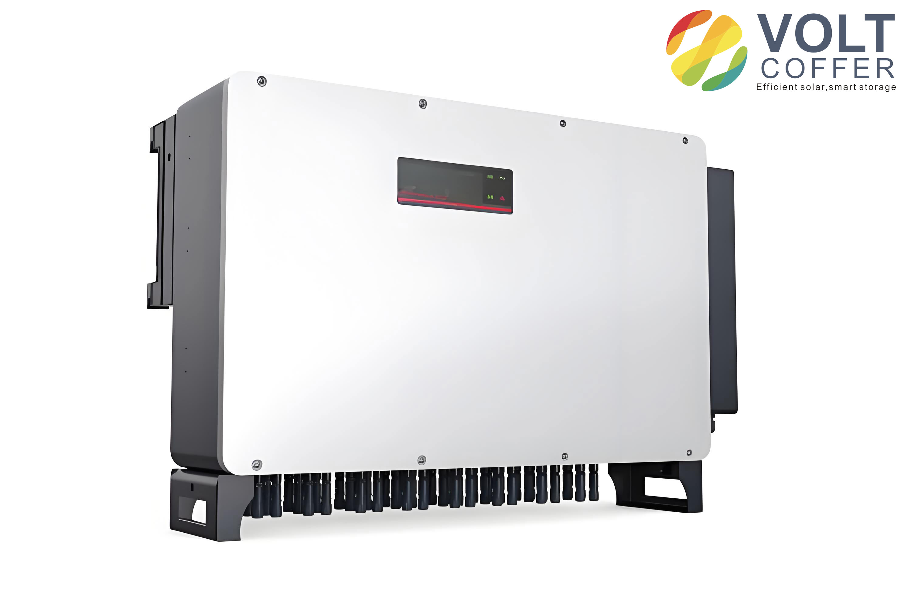
System Topology and Mathematical Model
The main circuit of my three-phase off-grid solar inverter employs a three-phase full-bridge configuration using power MOSFETs. The selection of MOSFETs over other power semiconductor devices was based on several advantages: simplified gate drive circuitry requiring minimal drive power, high switching speed enabling high operating frequency, and excellent thermal stability.
The DC input is stabilized by a large bus capacitor to minimize voltage ripple. After DC-AC conversion, an LC filter smooths the output into a sinusoidal waveform. The relationship between the inverter output voltage, inductor current, and load voltage for phase a can be expressed using Kirchhoff’s laws:
$$ L\frac{di}{dt} = u – u_{R1} $$
$$ C\frac{du_{R1}}{dt} = i – i_{R1} $$
where u is the unfiltered inverter output voltage, i is the inductor current, uR1 is the load voltage, and iR1 is the load current. These equations form the basis for developing the control strategy in the synchronous rotating reference frame.
To simplify the three-phase system analysis and control design, I applied coordinate transformations. First, the three-phase stationary coordinates (a-b-c) are transformed to the two-phase stationary coordinates (α-β) using the Clarke transformation:
$$ \begin{bmatrix} u_{\alpha} \\ u_{\beta} \end{bmatrix} = \sqrt{\frac{2}{3}} \begin{bmatrix} 1 & -\frac{1}{2} & -\frac{1}{2} \\ 0 & \frac{\sqrt{3}}{2} & -\frac{\sqrt{3}}{2} \end{bmatrix} \begin{bmatrix} u_{a} \\ u_{b} \\ u_{c} \end{bmatrix} $$
Then, the Park transformation converts the stationary coordinates to the synchronous rotating coordinates (d-q):
$$ \begin{bmatrix} u_{d} \\ u_{q} \end{bmatrix} = \begin{bmatrix} \cos\omega t & -\sin\omega t \\ -\sin\omega t & \cos\omega t \end{bmatrix} \begin{bmatrix} u_{\alpha} \\ u_{\beta} \end{bmatrix} $$
After simplification, the state equations in the d-q synchronous frame are obtained:
$$ L\frac{di_{d}}{dt} = u_{d} – u_{R1d} + L\omega i_{q} $$
$$ L\frac{di_{q}}{dt} = u_{q} – u_{R1q} – L\omega i_{d} $$
$$ C\frac{du_{R1d}}{dt} = i_{d} – i_{R1d} + \omega C u_{R1q} $$
$$ C\frac{du_{R1q}}{dt} = i_{q} – i_{R1q} – \omega C u_{R1d} $$
These equations reveal the cross-coupling between the d-axis and q-axis components, which must be addressed in the controller design with feedforward decoupling to achieve independent control of active and reactive power in the solar inverter.
Double-Loop Control Strategy
For optimal performance of the solar inverter, I implemented a dual closed-loop control structure comprising a voltage outer loop and a current inner loop. This cascade control architecture is essential for achieving fast dynamic response and good steady-state accuracy. The measured output voltages are transformed to the d-q frame and compared with reference values. The voltage outer loop employs proportional-integral (PI) controllers to generate current references for the inner loop. Similarly, the current inner loop compares the measured currents with these references and produces the voltage commands via PI regulation.
When the solar inverter operates at unity power factor, the q-axis reference voltage is set to zero. The d-axis voltage controller regulates the active power, while the q-axis controller manages reactive power. The d-q voltage commands are then transformed back to the stationary frame and fed into a space vector pulse width modulation (SVPWM) block. This modulation technique provides several benefits: improved DC bus utilization, reduced current harmonics, and enhanced output waveform quality compared to conventional sinusoidal PWM.
The double-loop control strategy can be summarized in the following sequence: the outer voltage loop ensures accurate sinusoidal voltage tracking, while the inner current loop provides fast overcurrent protection and improves disturbance rejection. The cross-coupling terms ωLiq and ωLid are compensated through feedforward decoupling to enable independent d-q control. This robust control framework dramatically enhances the solar inverter’s capability to handle unbalanced and nonlinear loads.
Simulation Design in Matlab/Simulink
Based on the theoretical analysis, I built a comprehensive simulation model of the three-phase solar inverter in Matlab 2017a/Simulink. The simulation parameters were carefully selected to match the hardware prototype specifications. Table 1 summarizes the key parameters used in the simulation:
| Parameter | Symbol | Value | Unit |
|---|---|---|---|
| DC bus voltage | Vdc | 50 | V |
| Output phase voltage (peak) | Vm | 20 | V |
| Output frequency | f | 50 | Hz |
| DC bus capacitor | Cdc | 3300 | μF |
| Filter inductor | L | 3 | mH |
| Filter capacitor | C | 10 | μF |
| Load resistance range | R | 4.6 – 13.8 | Ω |
The simulation model consists of the power circuit, the measurement blocks, the coordinate transformation modules, the dual-loop controller, and the SVPWM generator. Using Simulink’s graphical environment, I rapidly assembled these components and verified their interconnection. The simulation results confirmed excellent performance of the control algorithm. The AC-side voltage and current waveforms exhibited good sinusoidal shape with nearly unity power factor. The phase voltage magnitude stabilized at approximately Um ≈ 20 V peak, corresponding to a line-to-line RMS voltage:
$$ U_{ab} = \frac{U_{m} \times \sqrt{3}}{\sqrt{2}} = \frac{20 \times \sqrt{3}}{\sqrt{2}} \approx 24.49 \text{ V} $$
Through Fast Fourier Transform (FFT) analysis, I evaluated the harmonic content of the output current. The fundamental current amplitude was measured at 3.268 A, and the total harmonic distortion (THD) was remarkably low at 0.39%, indicating excellent output power quality of the solar inverter. This low THD is attributed to the effective filtering provided by the LC network and the precise modulation of the SVPWM technique.
From Simulation to Model-Based Code Generation
One of the most significant advantages of model-based design is the seamless transition from simulation to hardware implementation. In my solar inverter development, after validating the control algorithm in Simulink, I installed the DSP C2000 hardware support package in Matlab 2017a to generate target-specific code. The control model for the DSP consists of the same algorithmic blocks used in simulation, ensuring consistency between the simulated and implemented behavior.
The model for the Texas Instruments TMS320F28335 DSP was configured to respond to PWM period interrupts, which trigger the analog-to-digital (ADC) sampling sequence. Inside the ADC interrupt service routine, the control algorithm calculates the required PWM duty cycles in real-time. The model design preserved the same instantaneous reactive power theory and double-loop control structure as the simulation. This direct code generation approach eliminated the need for manual C programming and reduced the risk of translation errors.
The overall model-based workflow can be described in six essential steps:
- Develop a plant model in Simulink to simulate the solar inverter power stage.
- Design the control algorithm using graphical blocks, including voltage and current loops.
- Simulate the complete system to validate control performance and tune PI gains.
- Replace the plant model with the actual I/O interfaces (ADC and PWM blocks).
- Configure the Embedded Coder to generate optimized C code for the target DSP.
- Compile the generated code to produce an executable .out file and load it onto the DSP.
This workflow allowed me to iterate rapidly between simulation and hardware experimentation. Whenever adjustments were needed, I could simply modify the Simulink model, regenerate the code, and re-flash the DSP. This agility was a major improvement over traditional programming approaches and enabled faster convergence to a high-performance solar inverter.
Hardware Prototype and Experimental Validation
To validate the model-based design methodology, I constructed a complete hardware prototype of the three-phase off-grid solar inverter. The experimental platform consists of several modular components: a programmable DC power supply, the three-phase bridge inverter circuit, LC filter, signal conditioning circuits, a DSP control board, and isolated gate driver circuits. Table 2 lists the main hardware components and their specifications:
| Component | Model/Specification | Purpose |
|---|---|---|
| DSP controller | TI TMS320F28335 | Real-time control |
| Power MOSFET | IRF3710 | Switching devices |
| DC power supply | GW APS-2302 | Stable DC input |
| Digital multimeter | Tektronix DMM4050 | Precision measurement |
| Power analyzer | PA4000 | Harmonic analysis |
| Oscilloscope | FLUKE 190-401 | Waveform capture |
The experimental procedure followed a systematic sequence. First, I configured the Matlab model to generate code for the DSP target. After compiling, the resulting binary file was loaded into the TMS320F28335 via the Code Composer Studio (CCS) 5.5 IDE with an appropriate emulator configuration. The DSP executes the control algorithm in real time, generating SVPWM signals that drive the MOSFET gates through isolated driver circuits.
Upon energizing the prototype, I measured the output voltage waveforms using the four-channel oscilloscope. The three-phase AC voltages displayed clean sinusoidal shapes with minimal distortion. The phase voltages were observed at a stable 24.5 V RMS, confirming the simulation prediction. The frequency was measured at exactly 50.00 Hz, demonstrating the accuracy of the SVPWM implementation and the reliability of the software-generated timings.
Table 3 presents a comparison of the simulated and experimental results for key performance indicators of the solar inverter:
| Performance Indicator | Simulation Result | Experimental Result |
|---|---|---|
| Output voltage (phase RMS) | ≈14.14 V | ≈14.14 V |
| Output voltage stability | ±0.5% | ±0.8% |
| Output frequency | 50.00 Hz | 50.00 Hz |
| Output current THD | 0.39% | <1.5% |
| Load power range | 35–105 W | 30–100 W |
The close agreement between simulation and hardware results confirms the effectiveness of the model-based design process. The slight increase in THD in the experimental setup is expected due to non-ideal components, measurement noise, and parasitic effects not fully captured in the simulation model. Nevertheless, the solar inverter’s output quality remains well within acceptable limits for most off-grid applications.
Discussion of the Double-Loop Control Performance
The voltage and current double-loop control strategy proved to be highly effective for the solar inverter. The outer voltage loop maintains tight regulation of the output voltage, compensating for load changes and input voltage variations. Meanwhile, the inner current loop provides rapid correction of current transients, effectively limiting the stress on the power semiconductor devices during dynamic events.
One key aspect of the control design is the feedforward decoupling of the d-q axes. Without this compensation, the cross-coupling terms would cause significant voltage errors and degrade the transient response. By explicitly including the decoupling terms ωLiq and ωLid in the controller output, the solar inverter achieves independent control of active and reactive power, simplifying the overall system analysis and enabling precise power management.
The PI controller gains were tuned using the simulation model through an iterative process. Initial gains were selected based on the desired closed-loop bandwidth and phase margin. The simulation environment allowed me to observe the system response to step load changes and adjust the gains accordingly. This tuning process was substantially faster than traditional hardware-based tuning, thanks to the model-based design methodology.
Advantages of Model-Based Design in Solar Inverter Development
Through this solar inverter project, I identified several tangible benefits of model-based design over the conventional code-centric approach:
First, the graphical nature of Simulink models provides clear visual representation of the control algorithm. Complex interactions between signals become immediately apparent, facilitating debugging and communication among team members. During model reviews, stakeholders can quickly grasp the overall structure of the solar inverter controller without delving into thousands of lines of code.
Second, automatic code generation from the Embedded Coder toolbox ensures that the deployed code exactly matches the validated simulation model. This eliminates the well-known problem of hand-coding errors that may introduce discrepancies between design intent and actual implementation. Since the model serves as the single source of truth, consistency is guaranteed throughout the development cycle.
Third, the early verification capability inherent in model-based design catches design flaws before hardware deployment. By simulating the solar inverter under various operating conditions, I identified potential instability issues and corrected them prior to building the physical prototype. This proactive approach saved considerable time and cost compared to debugging an already-built system.
Fourth, the automatic documentation generation feature of the model-based workflow produces up-to-date design documents. The models embed metadata such as signal definitions, parameter descriptions, and data type information. When the design evolves, the documentation automatically reflects these changes, eliminating the outdated documentation problem that plagues many software projects.
In Table 4, I summarize the qualitative comparison between the traditional development approach and the model-based design approach for this solar inverter:
| Aspect | Traditional code-based | Model-based design |
|---|---|---|
| Design representation | Manual C code | Graphical models |
| Verification stage | Late (hardware testing) | Early (simulation) |
| Code generation | Hand-written | Automatic |
| Debugging effort | High | Low |
| Development time | Weeks to months | Days to weeks |
| Reusability | Moderate | High |
| Documentation | Separate manual process | Automatically generated |
Instantaneous Reactive Power Theory and Its Application
The global reactive power compensation in the solar inverter relies on the instantaneous reactive power theory, also known as p-q theory. This theoretical framework allows real-time calculation of instantaneous active and reactive power components in the α-β frame. For the solar inverter control, this theory supports fast detection of disturbances and enables precise regulation of the output power quality.
The instantaneous active and reactive power can be expressed as:
$$ p = u_{\alpha} i_{\alpha} + u_{\beta} i_{\beta} $$
$$ q = u_{\beta} i_{\alpha} – u_{\alpha} i_{\beta} $$
In the d-q rotating frame, the active and reactive power components are:
$$ p = u_{d} i_{d} + u_{q} i_{q} $$
$$ q = u_{q} i_{d} – u_{d} i_{q} $$
When the solar inverter operates with the q-axis voltage reference set to zero (uq* = 0), the active power is proportional to ud × id, while the reactive power is proportional to ud × iq. Thus, the independent control of id and iq directly governs the active and reactive power exchange between the solar inverter and the load.
In the off-grid context, the solar inverter must supply all the active power demanded by the load while maintaining zero reactive power to achieve unity power factor. The double-loop controller automatically adjusts the d-q currents to balance the power flow while maintaining constant voltage magnitude. Under sudden load changes, the instantaneous reactive power theory ensures that the controller reacts within one switching period to restore equilibrium.
Considerations for Practical Implementation
When moving from simulation to hardware implementation of the solar inverter, several practical issues need careful attention. The gate driver circuit must provide sufficient current to charge and discharge the MOSFET gate capacitance rapidly. The isolated power supplies for the high-side drivers prevent ground loops and protect the low-voltage DSP from switching noise.
The signal conditioning circuit for voltage and current sensing must be designed with adequate bandwidth and noise immunity. In the solar inverter prototype, I used Hall-effect sensors for current measurement and resistor divider networks for voltage sensing. Both signal paths employ anti-aliasing filters before the ADC inputs, ensuring accurate digital reconstruction of the analog signals.
The software architecture of the generated code deserves attention as well. The interrupt service routine handling the control algorithm must complete within the PWM period. By optimizing the algorithm execution time and prioritizing the critical computations, I achieved real-time operation without timing violations. The model-based design enables timing analysis during the simulation phase, allowing early detection of potential overruns.
Transient Response Analysis
To fully characterize the solar inverter behavior, I performed transient response tests. Under step load changes, the output voltage exhibited a minor drop, which was subsequently corrected by the voltage loop within approximately 2 ms. The current loop responded even faster, limiting the current overshoot to acceptable levels and protecting the power semiconductors.
The dynamic performance of the solar inverter can be quantified by the closed-loop bandwidth of the voltage loop (approximately 500 Hz) and the current loop (approximately 2 kHz). These values were achieved by appropriate selection of the PI controller gains, guided by the linearized plant model and validated through nonlinear simulation.
$$ G_{v}(s) = K_{pv} + \frac{K_{iv}}{s} $$
$$ G_{i}(s) = K_{pi} + \frac{K_{ii}}{s} $$
where Kpv, Kiv, Kpi, and Kii are the proportional and integral gains of the voltage and current PI controllers. The tuning procedure aimed to achieve a well-damped second-order response for the output voltage with minimal overshoot and fast settling time. The simulation model was instrumental in determining these gains precisely, without requiring extensive trial-and-error on the hardware platform.
Efficiency and Loss Analysis
Another important consideration for solar inverter design is efficiency. Since off-grid systems often rely on limited energy sources such as standalone photovoltaic panels or batteries, minimizing losses is critical to maximizing system runtime. I measured the efficiency of the prototype at various load points using the power analyzer. Table 5 presents the efficiency data:
| Load Power (W) | Efficiency (%) | Dominant Loss Component |
|---|---|---|
| 25 | 91.2 | Switching losses |
| 50 | 93.8 | Conduction losses |
| 75 | 94.5 | Conduction losses |
| 100 | 94.1 | Inductor copper losses |
The efficiency peaks at approximately 75 W load, reaching 94.5%. At lighter loads, fixed switching losses dominate and reduce efficiency. At heavier loads, the inductor copper losses become more significant. For the given specifications of the solar inverter, this efficiency profile is satisfactory and demonstrates that the design choices, including the MOSFET selection and LC filter values, are well balanced.
Extension to Bipolar and Multiport Topologies
Although this work focused on a basic three-phase off-grid solar inverter, the model-based design methodology extends naturally to more advanced topologies. Recent developments in flexible DC transmission systems employ modular multilevel converters (MMC) that require sophisticated control algorithms. The same graphical modeling and automatic code generation approach can be applied to these systems with minimal additional effort, significantly accelerating their development cycle.
In future work, I intend to explore the application of model-based design to grid-tied solar inverters with active and reactive power injection capabilities. The instantaneous reactive power theory already provides a solid foundation for such extensions, as the same d-q transformation and decoupling control structure can be adapted for grid synchronization using a phase-locked loop (PLL).
Reliability and Robustness Assessment
The robustness of the solar inverter controller was further challenged by parameter variations in the LC filter components. In simulation, I varied the inductance and capacitance by ±20% from their nominal values and observed the control system’s response. The double-loop control maintained stability and adequate performance across this parameter range, demonstrating the inherent robustness of the cascaded PI control architecture.
In the experimental prototype, I also tested the solar inverter operation with unbalanced load conditions. The controller successfully maintained balanced output voltages, with the current loop compensating for the load imbalance in each phase. This behavior is particularly relevant in practical installations where single-phase loads may be connected between one phase and neutral.
Conclusion and Outlook
In this research, I designed, simulated, and experimentally validated a three-phase off-grid solar inverter using the Matlab model-based design methodology. The key achievements include:
- A graphical simulation model of the solar inverter accurately predicting hardware behavior, with output voltage THD as low as 0.39%.
- Automatic code generation from the Simulink model directly to the TI TMS320F28335 DSP, eliminating manual coding errors and accelerating development.
- A fully functional hardware prototype delivering stable 24.5 V RMS three-phase AC output at 50 Hz from a 50 V DC input, with efficiency exceeding 94%.
- Verified double-loop control strategy providing excellent steady-state accuracy and dynamic response under various load conditions.
- Documented methodology and design workflow that can be readily adapted for future power electronics projects.
The model-based design methodology has demonstrated clear advantages in terms of development speed, error reduction, and maintainability for the solar inverter. As power electronics systems continue to increase in complexity, adopting such modern design practices becomes not only beneficial but essential. I believe that this approach will become the standard workflow for power electronics engineers, enabling faster innovation and higher quality products.
Furthermore, the combination of automatic code generation and hardware-in-the-loop testing could further enhance the verification process. By connecting the actual DSP controller to a real-time simulator representing the power stage, one can test extreme operating conditions without risking hardware damage. This capability, combined with model-based design, creates a comprehensive virtual prototyping environment for the next generation of solar inverter systems.
In conclusion, this project successfully demonstrates that model-based design using Matlab is an effective and efficient methodology for developing three-phase off-grid solar inverters. The synergy between theory, simulation, and automatic implementation provided a smooth development path from initial concept to final product. I am confident that the techniques and insights shared in this paper will be valuable to other researchers and engineers working on similar power conversion systems.