
In this thesis, I systematically investigated a resonant bidirectional DC/DC converter dedicated to energy storage system applications. The rapid growth of renewable energy penetration and the urgent need for carbon neutrality have placed higher demands on the reliability and efficiency of energy storage system. A bidirectional DC/DC converter is the key interface between the energy storage unit and the DC bus, and its performance directly affects the overall system stability, power density, and energy conversion efficiency. In my research, I proposed a two-stage cascaded converter topology, consisting of a front-stage bidirectional resonant converter and a rear-stage three-phase interleaved Buck/Boost converter. I carried out detailed theoretical analyses, small-signal modeling, control strategy design, simulation verification, and experimental validation. The results demonstrated that the proposed converter can achieve soft switching, bidirectional power flow, low output ripple, and high efficiency, which makes it highly suitable for energy storage system applications.
1. Introduction
The global energy landscape is undergoing a profound transformation. With the increasing depletion of fossil fuels and the continuous growth of energy demand, the development of renewable energy sources such as solar and wind has become a common goal for countries around the world. However, the intermittent and stochastic nature of these renewable sources introduces significant challenges to the stable operation of power grids. To address these challenges, microgrids and smart grids have been proposed as effective solutions, and among them, the DC microgrid has attracted particular attention due to its inherent advantages in interfacing with DC-based renewable generation, energy storage, and modern electronic loads. In a DC microgrid, the energy storage system plays a vital role in balancing power generation and consumption. When the generated power exceeds the load demand, the excess energy is stored in the battery; conversely, when the load demand exceeds the generated power, the stored energy is released to support the DC bus voltage. The bidirectional DC/DC converter is the central component that enables this energy exchange between the storage device and the DC bus.
In general, bidirectional DC/DC converters can be classified into two categories: isolated and non-isolated topologies. Non-isolated converters, such as Buck-Boost, Cuk, Sepic-Zeta, and four-switch Buck-Boost, offer simple structures and low cost, but they lack galvanic isolation and usually suffer from limited voltage gain ranges. Isolated converters, such as Dual Active Bridge (DAB), series resonant converter (SRC), parallel resonant converter (PRC), LLC, CLLC, and CLLLC, provide electrical isolation and can achieve high voltage conversion ratios through the transformer turns ratio. Among these, resonant converters are particularly attractive because they can realize zero-voltage switching (ZVS) and zero-current switching (ZCS), thereby reducing switching losses and electromagnetic interference. Nevertheless, some traditional resonant topologies have limitations in terms of bidirectional voltage gain symmetry and control complexity. For example, the conventional LLC resonant converter has an asymmetric gain characteristic when operated in the reverse direction, which restricts its application in bidirectional energy storage system. In my work, I aimed to propose a resonant bidirectional DC/DC converter topology that preserves the advantages of soft switching and wide voltage gain while maintaining a simple structure and symmetrical operation.
2. System Configuration and Operating Principles
2.1 Overall Topology
The proposed bidirectional DC/DC converter system is illustrated conceptually in this section. The overall structure is composed of two cascaded power stages: the front-stage bidirectional resonant converter and the rear-stage three-phase interleaved Buck/Boost converter. The front-stage converter is responsible for isolating the high-voltage side from the low-voltage side and for providing a stable DC bus voltage. The rear-stage converter interfaces with the battery or low-voltage load and performs the function of voltage regulation and current sharing. The bidirectional power flow capability allows the energy storage system to operate in both charging (forward) and discharging (reverse) modes.
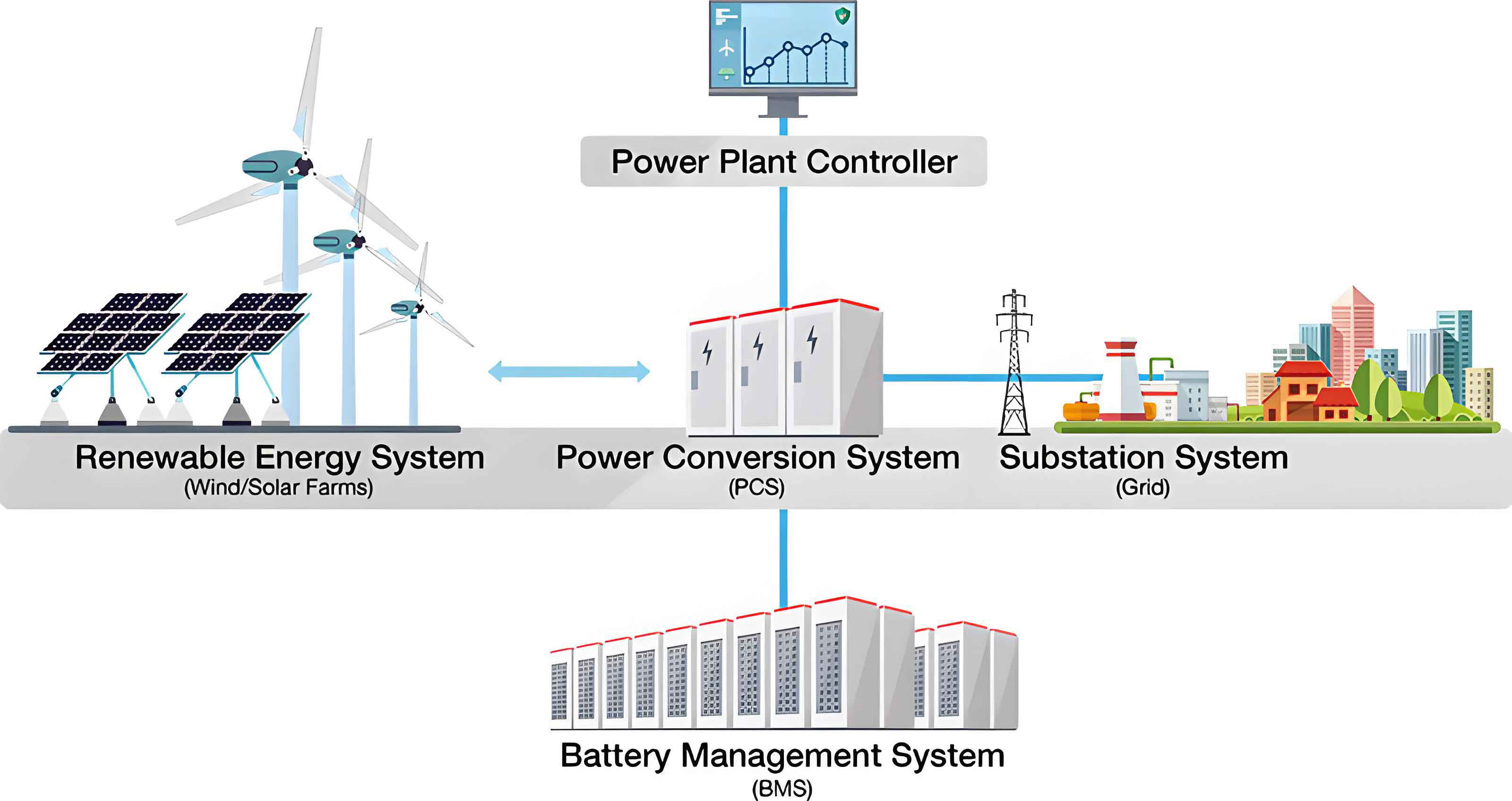
A typical configuration of an energy storage system based on a DC microgrid is illustrated above. The energy storage system is connected to the DC bus through the proposed bidirectional DC/DC converter. In the forward mode, power flows from the high-voltage DC bus to the low-voltage battery side, enabling charging. In the reverse mode, power flows from the battery to the DC bus, enabling discharging. The two-stage design allows the front-stage resonant converter to handle the wide input voltage range and provide isolation, while the rear-stage interleaved converter reduces current ripple and improves the current-sharing capabilities.
2.2 Front-stage Bidirectional Resonant Converter
The front-stage converter is a full-bridge resonant topology with a symmetric structure. It consists of eight power switches, a resonant capacitor \(C_r\), a resonant inductor \(L_r\), an auxiliary inductor \(L\), a magnetizing inductor \(L_m\), a high-frequency transformer with turns ratio \(n\), and input/output capacitors. The switches \(S_1-S_4\) form the primary full bridge, and \(S_5-S_8\) form the secondary full bridge. The antiparallel diodes and parasitic capacitors of the switches are utilized to achieve soft switching.
In the forward operating mode, the auxiliary inductor \(L\) is clamped by the primary-side voltage and does not participate in resonance. The resonant frequency in this mode is given by:
$$ f_{r1} = \frac{1}{2\pi \sqrt{L_r C_r}} \sqrt{\frac{L_m}{L_m + L_r}} $$
In the reverse operating mode, the auxiliary inductor \(L\) participates in resonance, and the resonant frequency becomes:
$$ f_{r2} = \frac{1}{2\pi \sqrt{(L_r+L) C_r}} $$
I analyzed the operating principles of the front-stage converter in both directions. In the forward mode, depending on the relationship between the switching frequency \(f_s\) and the resonant frequency \(f_{r1}\), the converter can operate in three states: below resonance (\(f_s < f_{r1}\)), at resonance (\(f_s = f_{r1}\)), and above resonance (\(f_s > f_{r1}\)). I focused on the two states that allow ZVS of the primary-side switches. During the dead-time interval, the parasitic capacitors of the switches are charged and discharged by the resonant current, enabling ZVS turn-on. In the below-resonance state, the secondary-side diodes achieve ZCS because the secondary current naturally drops to zero before the end of the half-cycle.
To derive the voltage gain characteristics, I employed the fundamental harmonic approximation (FHA) method. The equivalent AC resistance seen from the primary side is:
$$ R_{eq}’ = \frac{8 n^2}{\pi^2} R_{dc} $$
where \(R_{dc}\) is the equivalent load resistance at the output. The forward voltage gain \(M(f_n, Q, k_1)\) is obtained as:
$$ M(f_n, Q, k_1) = \frac{1}{\sqrt{ \left(1 + \frac{1}{k_1} – \frac{1}{k_1 f_n^2}\right)^2 + Q^2 \left( f_n – \frac{1}{f_n}\right)^2 }} $$
where \(f_n = f_s / f_{r1}\), \(k_1 = L_m / L_r\), and \(Q = Z_r / R_{eq}’\) with \(Z_r = \sqrt{L_r / C_r}\). I plotted the gain curves for different values of \(k_1\) and \(Q\). The results show that at \(f_n = 1\), the gain is not unity but depends on \(k_1\). A larger \(k_1\) reduces the gain and shifts the peak frequency leftward. Therefore, I selected \(k_1 = 5\) to achieve a wide gain range while maintaining reasonable control complexity.
Similarly, for the reverse mode, I derived the voltage gain expression as:
$$ M(f_n, Q, k_1, k_2) = \frac{1}{\sqrt{ \left(1 + \frac{1}{k_1} + \frac{1}{k_2} – \frac{1}{k_1 f_n^2}\right)^2 + Q^2 \left( f_n – \frac{1}{f_n}\right)^2 }} $$
where \(k_2 = L / L_r\). I selected \(k_2 = 4\) to satisfy the reverse gain requirement. The quality factor \(Q\) was chosen as 0.3 for the forward mode and 0.45 for the reverse mode, based on the gain analysis and soft-switching constraints.
2.3 Rear-stage Three-Phase Interleaved Buck/Boost Converter
The rear-stage converter is a three-phase interleaved synchronous Buck/Boost converter. It consists of six switches \(S_9-S_{14}\), three inductors \(L_1\), \(L_2\), \(L_3\), and input/output capacitors. The interleaving technique is used to reduce the current ripple on both input and output sides. The phase shift between adjacent phases is \(120^\circ\), which effectively cancels a large portion of the low-frequency ripple components.
In the Buck mode (forward power flow), the high-side switches \(S_9\), \(S_{11}\), and \(S_{13}\) are controlled with the same duty cycle \(D\) but phase shifted by \(120^\circ\). The low-side switches \(S_{10}\), \(S_{12}\), and \(S_{14}\) operate complementarily. I analyzed the converter operation for three duty cycle ranges: \(D \le 1/3\), \(1/3 < D \le 2/3\), and \(2/3 < D \le 1\). The inductor voltage equations for each interval are derived using the state-space averaging method. For example, when \(D \le 1/3\), the output current ripple \(\Delta i_{o\_Buck}\) is:
$$ \Delta i_{o\_Buck} = \frac{V_{dc} D T_s}{L} (1-3D) $$
where \(T_s\) is the switching period. The output voltage ripple \(\Delta v_o\) is:
$$ \Delta v_o = \frac{V_o T_s^2 D (1-3D)}{48 C_o L} $$
For the Boost mode (reverse power flow), the low-side switches \(S_{10}\), \(S_{12}\), and \(S_{14}\) are controlled with duty cycle \(D’\), while the high-side switches operate complementarily. The current ripple expressions are analogous to those of the Buck mode with the substitution \(D’ = 1-D\). I defined the ripple reduction factors \(K_{io}(D)\) and \(K_{vo}(D)\) to quantify the improvement introduced by the three-phase interleaving. The analysis shows that the output current ripple is always less than the single-phase inductor current ripple, and at \(D = 1/3\) or \(2/3\), the voltage ripple becomes zero, which is a significant advantage of the proposed topology.
2.4 Ripple Analysis and Summary
To summarize the key performance metrics of the rear-stage converter, I constructed Table 2.1 below.
| Parameter | Expression (Buck Mode) | Expression (Boost Mode) |
|---|---|---|
| Inductor current ripple | \(\Delta i_{L\_Buck} = \frac{V_{dc} – V_o}{L} D T_s\) | \(\Delta i_{L\_Boost} = \frac{V_o}{L} D’ T_s\) |
| Output current ripple | \(\Delta i_{o\_Buck} = \frac{V_{dc} D T_s}{L} (1-3D)\) for \(D \le 1/3\) | \(\Delta i_{o\_Boost} = \frac{V_o D’ T_s}{L} (1-3D’)\) for \(D’ \le 1/3\) |
| Output voltage ripple | \(\Delta v_o = \frac{V_o T_s^2 D (1-3D)}{48 C_o L}\) | \(\Delta v_{dc} = \frac{V_{dc} T_s D’ (1-3D’)}{6 C_{dc} R}\) |
These equations confirm that the three-phase interleaved topology significantly reduces the output current and voltage ripples, which is essential for high-quality power delivery in energy storage system applications.
3. Parameter Design and Device Selection
3.1 Front-stage Converter Design
The design specifications of the front-stage converter are listed in Table 3.1.
| Parameter | Symbol | Value |
|---|---|---|
| Input voltage range | \(V_{in}\) | 320–480 V |
| Rated input voltage | \(V_{in\_nom}\) | 400 V |
| DC bus voltage range | \(V_{dc}\) | 36–60 V |
| Rated DC bus voltage | \(V_{dc\_nom}\) | 48 V |
| Rated output power | \(P\) | 1.2 kW |
| Target efficiency | \(\eta\) | \(\ge 95\%\) |
I first determined the resonant frequency. The conventional LLC resonant frequency was set to 100 kHz. With the selected \(k_1 = 5\), the actual forward resonant frequency \(f_{r1}\) becomes about 110 kHz. The transformer turns ratio \(n\) was derived from the required voltage gain at resonance. At \(f_n = 1\), the gain \(M\) is about 1.2 for \(k_1 = 5\). Thus:
$$ n = \frac{M V_{in}}{V_{dc}} = \frac{1.2 \times 400}{48} = 10 $$
The magnetizing inductance \(L_m\) was selected to satisfy both the voltage gain requirement and the ZVS condition. I plotted the gain curves for different \(L_m\) values and selected \(L_m = 410\,\mu H\). The ZVS constraint is:
$$ L_m \le \frac{t_{dead}}{8 C_{oss} f_{r1}} $$
where \(t_{dead} = 200\,ns\) and \(C_{oss} = 350\,pF\). The selected \(L_m = 410\,\mu H\) satisfies this condition. Then, the resonant inductance referred to the primary side is:
$$ L_r’ = \frac{L_m}{k_1} = 82\,\mu H $$
The actual secondary-side resonant inductance is:
$$ L_r = \frac{L_r’}{n^2} = 0.82\,\mu H $$
The resonant capacitance is:
$$ C_r = \frac{1}{(2\pi f_{r1})^2 L_r’} \approx 25.6\,nF $$
For the reverse mode, I selected the auxiliary inductance \(L = 45\,\mu H\) to provide sufficient voltage gain when the converter operates in the reverse direction. The DC bus capacitor was designed to maintain the bus voltage for a hold-up time of 20 ms. Using the energy balance equation, I selected \(C_{dc} = 200\,\mu F\).
3.2 Device Selection for the Front-stage Converter
The power switches of the front-stage converter must withstand a maximum voltage of 480 V on the primary side and about 60 V on the secondary side. Considering a 1.5 safety margin, the primary switches need a voltage rating of at least 720 V. I selected IRFPE50 MOSFETs, which have a drain-source breakdown voltage of 800 V and a continuous drain current of 17 A. For the secondary-side switches, a voltage rating of 100 V is sufficient; however, for simplicity and availability, I also used IRFPE50 for the secondary full bridge, which provides adequate margin. The parasitic capacitance \(C_{oss} = 350\,pF\) and the dead time \(t_{dead} = 200\,ns\) were used to verify the ZVS condition.
The high-frequency transformer was designed using the AP method. The required area product is:
$$ AP = \frac{P_T \times 10^4}{k_w k_f J B_{max} f_{r1}} = 2.57\,cm^4 $$
where \(P_T = P(1+1/\eta) \approx 2463\,W\). I selected the EE42 core with \(AP = 4.615\,cm^4\), effective area \(A_e = 233\,mm^2\), and window area \(A_w = 264.25\,mm^2\). The secondary side turns were calculated as:
$$ N_s = \frac{V_{dc} \times 10^4}{k_f B_{max} A_e f_{r1}} = 2.34 $$
I chose \(N_s = 3\) turns, and the primary side turns is \(N_p = n N_s = 30\) turns. To reduce the skin effect, I used Litz wire with a strand diameter of 0.3 mm. The primary winding uses 11 strands and the secondary winding uses 90 strands, resulting in a window utilization factor of 0.146, which is acceptable.
For the resonant inductor \(L_r\) and auxiliary inductor \(L\), I used the AP method and selected EE24 cores. The required number of turns for \(L\) is 17 and for \(L_r\) is 3. The resonant capacitor \(C_r\) was chosen as a polypropylene film capacitor with a voltage rating of 1500 V, which provides ample margin.
3.3 Rear-stage Converter Design
The design specifications for the rear-stage converter are listed in Table 3.2.
| Parameter | Symbol | Value |
|---|---|---|
| Input DC bus voltage | \(V_{dc}\) | 36–60 V |
| Rated bus voltage | \(V_{dc\_nom}\) | 48 V |
| Output voltage range | \(V_o\) | 20–28 V |
| Rated output voltage | \(V_o\_nom\) | 24 V |
| Rated output power | \(P\) | 1.2 kW |
| Switching frequency | \(f_{s\_rear}\) | 50 kHz |
| Inductor current ripple | \(\Delta i_L\) | <10% |
| Output current ripple | \(\Delta i_o\) | <2% |
For the Buck mode, the duty cycle range is:
$$ D_{min} = \frac{V_{o\_min}}{V_{dc\_max}} = \frac{20}{60} \approx 0.333 $$
$$ D_{max} = \frac{V_{o\_max}}{V_{dc\_min}} = \frac{28}{36} \approx 0.778 $$
The critical inductor value is determined by the maximum current ripple. With a desired \(\Delta i_L = 1.667\,A\), the required inductance is:
$$ L_{min} = \frac{(V_{dc} – V_o) D T_s}{\Delta i_L} = 23.99\,\mu H $$
For the Boost mode, the duty cycle range is:
$$ D’_{min} = 1 – \frac{V_{o\_max}}{V_{dc\_min}} = 1 – \frac{28}{36} \approx 0.222 $$
$$ D’_{max} = 1 – \frac{V_{o\_min}}{V_{dc\_max}} = 1 – \frac{20}{60} \approx 0.667 $$
The minimum inductance in Boost mode is 21.12 μH. To provide sufficient margin, I selected \(L_1 = L_2 = L_3 = 40\,\mu H\). The output filter capacitor was designed to limit the voltage ripple to 2% of the nominal output voltage. Using the worst-case duty cycle, I selected \(C_o = 16\,\mu F\). The DC bus capacitor \(C_{dc}\) is shared from the front-stage converter and is 200 μF.
3.4 Device Selection for the Rear-stage Converter
The power switches in the rear-stage converter need to withstand a maximum drain-source voltage equal to the DC bus voltage, which is 60 V. Considering a 1.5 safety margin, the voltage rating should be at least 90 V. I selected IRFP260NPBF MOSFETs, which have a breakdown voltage of 200 V and a continuous drain current of 50 A. This device provides sufficient margin for the 16.67 A output current and the transient overload conditions. The low on-resistance of these devices helps to minimize conduction losses, contributing to the high overall efficiency of the energy storage system.
4. Control Strategies and Simulation Analysis
4.1 Overall Control Structure
The control system of the proposed bidirectional DC/DC converter is designed to achieve stable voltage regulation, fast dynamic response, and balanced current sharing. The overall control diagram is divided into three main parts: the front-stage resonant converter controller, the rear-stage Buck/Boost controller, and the PWM duty-cycle distribution module. The front-stage controller operates in two modes. In the forward mode, it maintains the DC bus voltage at 48 V using a voltage-current double closed-loop control. In the reverse mode, it regulates the input voltage to 400 V. The rear-stage controller also has two modes: in the Buck mode, it regulates the output voltage to 24 V; in the Boost mode, it regulates the DC bus voltage to 48 V. To realize current sharing among the three interleaved phases, I adopted a control strategy that performs a secondary distribution of the duty cycle generated by the conventional current loop. This method preserves the simplicity of the traditional PI controller while effectively balancing the phase currents.
4.2 Small-Signal Modeling of the Front-stage Converter
Because the state variables of the resonant converter contain both AC and DC components, I used the extended describing function method to derive the small-signal model. I defined the sinusoidal and cosine components of the resonant inductor current, the magnetizing current, and the resonant capacitor voltage. By applying harmonic balance, I obtained the steady-state equations. After linearization around the operating point, the state-space model can be expressed as:
$$ \frac{d\hat{x}}{dt} = \mathbf{A}\hat{x} + \mathbf{B}\hat{u} $$
$$ \hat{y} = \mathbf{C}\hat{x} + \mathbf{D}\hat{u} $$
For the forward mode, the state vector is:
$$ \hat{x} = [\hat{i}_{rs}, \hat{i}_{rc}, \hat{v}_{Crs}, \hat{v}_{Crc}, \hat{i}_{ms}, \hat{i}_{mc}, \hat{v}_{Cdc}]^T $$
and the input is \(\hat{u} = [\hat{v}_{in}, \hat{\omega}_s]^T\). The output is \(\hat{y} = [\hat{v}_{dc}]\). I computed the transfer function from the switching frequency perturbation to the output voltage, denoted as \(G_{dc}(s)\). Similarly, for the reverse mode, I derived the transfer function \(G_{in}(s)\) using the same method. These transfer functions were used to design the PI compensators.
4.3 Small-Signal Modeling of the Rear-stage Converter
For the rear-stage converter, I applied the conventional state-space averaging with small-signal perturbation. In the Buck mode, the small-signal equations are:
$$ L \frac{d\hat{i}_{L1}}{dt} = D\hat{v}_{dc} + V_{dc}\hat{d}_1 – \hat{v}_o $$
$$ L \frac{d\hat{i}_{L2}}{dt} = D\hat{v}_{dc} + V_{dc}\hat{d}_3 – \hat{v}_o $$
$$ L \frac{d\hat{i}_{L3}}{dt} = D\hat{v}_{dc} + V_{dc}\hat{d}_5 – \hat{v}_o $$
$$ C_o \frac{d\hat{v}_o}{dt} = \hat{i}_{L1} + \hat{i}_{L2} + \hat{i}_{L3} – \frac{\hat{v}_o}{R} $$
Assuming identical phases, I obtained the control-to-inductor-current transfer function \(G_{id}(s)\) and the control-to-output-voltage transfer function \(G_{vd}(s)\). For the Boost mode, the small-signal equations are similar with the complementary duty cycle \(D’\). The resulting transfer functions were used to design the current loop and voltage loop compensators.
4.4 Duty-Cycle Secondary Distribution for Current Sharing
To achieve current sharing among the three phases, I proposed a duty-cycle secondary distribution method. The conventional voltage-current double-loop controller generates a common duty cycle \(D\). This common duty cycle is then modified by adding a phase-specific correction \(\Delta D_i\) based on the difference between the phase inductor current \(i_{Li}\) and one-third of the total output current \(i_o/3\). The correction is:
$$ \Delta D_i = K_p \left( i_{Li} – \frac{i_o}{3} \right) $$
where \(K_p\) is a proportional gain. The final duty cycle for each phase is:
$$ D_i = D + \Delta D_i $$
By maintaining the sum of the corrections equal to zero, the average output voltage remains unaffected while the individual phase currents are balanced. I implemented this algorithm digitally in the DSP. The control block diagram is shown conceptually in the simulation section.
4.5 Controller Design and Bode Analysis
I used MATLAB to design the PI controllers and to analyze the closed-loop stability. For the front-stage resonant converter, the Bode plot of the uncompensated system showed a crossover frequency of \(5.01 \times 10^3\) rad/s and a phase margin of 38.8°. I designed a PI compensator with \(k_p = 0.2\) and \(k_i = 2000\), which increased the low-frequency gain and reduced the crossover frequency to \(9.98 \times 10^2\) rad/s while maintaining a phase margin of 35.7°. For the reverse mode, the compensator was designed similarly. For the rear-stage converter, I designed the current loop first. The uncompensated current loop had a crossover frequency of \(1.08 \times 10^6\) rad/s with a phase margin of 89.8°. I designed a PI compensator to achieve a crossover frequency of \(3.05 \times 10^4\) rad/s and a phase margin of 60°. Then, I designed the voltage loop. The uncompensated voltage loop had a crossover frequency of \(1.25 \times 10^4\) rad/s. After adding the PI compensator, the crossover frequency became \(4 \times 10^4\) rad/s with a phase margin of 56°. For the Boost mode, similar procedures were followed. The final PI parameters are summarized in Table 4.1.
| Loop | Mode | \(k_p\) | \(k_i\) | Phase margin |
|---|---|---|---|---|
| Front-stage voltage | Forward | 0.2 | 2000 | 35.7° |
| Front-stage voltage | Reverse | 0.15 | 1500 | 38.5° |
| Rear-stage current | Buck | 0.8 | 10000 | 60° |
| Rear-stage voltage | Buck | 2.0 | 50000 | 56° |
| Rear-stage current | Boost | 0.6 | 8000 | 62.6° |
| Rear-stage voltage | Boost | 1.5 | 40000 | 54.3° |
4.6 Simulation Results
I built a comprehensive simulation model in MATLAB/Simulink to verify the theoretical analysis. The simulation model includes the full power stage, the control blocks, and the PWM generation. I first simulated the forward mode with an input voltage of 400 V. The waveforms of the gate signal \(V_{gs1}\), drain-source voltage \(V_{ds1}\), and resonant current \(i_{Cr}\) are shown in the simulation. The results confirmed that \(V_{ds1}\) is zero when the gate signal is applied, demonstrating ZVS operation. The DC bus voltage stabilized at 48 V with a ripple of about 0.08 V, which is within the design specification.
To verify the effectiveness of the duty-cycle secondary distribution current sharing method, I intentionally added different parasitic resistances in the three phases. Under the conventional double closed-loop control, the three phase currents were significantly unbalanced. With the proposed duty-cycle redistribution, the three phase currents became almost equal. The total output current ripple was also reduced, confirming the effectiveness of the interleaving and current sharing control.
I also tested the dynamic response of the system. When a 5% step disturbance was applied to the input voltage, the output voltage recovered to 24 V within a short time. When a load step was applied, the output voltage experienced a small transient and returned to the reference value in about 3 ms. These results validate the excellent dynamic performance of the proposed control strategy.
For the reverse mode, the input voltage was set to 24 V. The three-phase inductor currents were well balanced, and the DC bus voltage was regulated at 48 V. The front-stage resonant converter again demonstrated ZVS and ZCS. A 5% input voltage disturbance was applied, and the output voltage quickly returned to 400 V, showing good disturbance rejection capability.
5. Hardware Design and Experimental Verification
5.1 Hardware Circuit Design
To further validate the design, I constructed a 1.2 kW experimental prototype. The hardware platform consists of the power stage, gate driver circuits, voltage and current sampling circuits, auxiliary power supplies, and a digital signal processor (TMS320F28335). The following subsections briefly describe the key hardware designs.
5.1.1 Gate Driver Circuit
The gate driver circuit uses the UCC21520 driver chip. This chip provides two isolated channels with a peak source current of 4 A and a sink current of 6 A, which is sufficient to charge and discharge the gate capacitance of the selected MOSFETs. I used a +15 V/-3.5 V gate drive voltage to ensure fast switching and reliable turn-off. The dead-time between complementary signals was set to 200 ns. The driver circuit was designed with isolated power supplies to provide the required unipolar and bipolar voltages.
5.1.2 Voltage Sampling Circuit
I used the NSI1311 isolated amplifier for voltage sensing. The input voltage is divided by a resistor network and then fed to the isolated amplifier. The output of the amplifier is scaled by an operational amplifier AD8601 and then sent to the ADC of the DSP. A zener diode protects the ADC input from overvoltage.
5.1.3 Current Sampling Circuit
The current sensing is performed using shunt resistors and the INA181 current sense amplifier. The voltage drop across the shunt is filtered and amplified before being fed to the ADC. The circuit provides a high bandwidth and accurate current measurement for both the inductor currents and the total output current.
5.2 Software Design
The control algorithm is implemented in the TMS320F28335 DSP. The main program initializes the system clock, GPIO, ADC, EPWM modules, and interrupts. The interrupt service routine performs the following tasks: reads the ADC samples, checks for overcurrent/overvoltage conditions, executes the voltage and current control loops, applies the duty-cycle secondary distribution algorithm, and updates the PWM registers. The program flow is straightforward and ensures real-time control.
5.3 Experimental Results
I conducted a series of experiments to verify the theoretical and simulation results. In the forward mode, with an input voltage of 400 V, I measured the gate signal \(V_{gs1}\), drain-source voltage \(V_{ds1}\), and resonant current \(i_{Cr}\). The experimental waveforms confirm that the switch turns on with zero voltage across it, thus verifying ZVS. The secondary-side diode currents \(i_{Dq5}\) and \(i_{Dq7}\) also fall to zero naturally, confirming ZCS.
The DC bus voltage was measured at 48 V, which matches the design value. The three-phase inductor currents \(i_{L1}\), \(i_{L2}\), and \(i_{L3}\) were recorded. With the duty-cycle secondary distribution, the three currents were essentially equal, with a ripple below 4 A. The total output current ripple was significantly smaller than the single-phase ripple, as designed.
I also measured the output voltage during a 5% input voltage disturbance. The output voltage remained almost constant at 24 V, demonstrating excellent disturbance rejection. The load transient response showed a rapid recovery within a few milliseconds, validating the dynamic performance.
In the reverse mode, the input voltage was set to 24 V. The three-phase inductor currents were balanced, and the output voltage was regulated at 48 V. The resonant converter again achieved ZVS and ZCS, as evidenced by the diode current waveforms. The output voltage was measured at 400 V for the front-stage converter, confirming the bidirectional power transfer capability.
Finally, I measured the efficiency of the entire bidirectional DC/DC converter system for different power levels. Table 5.1 summarizes the measured efficiency at selected power points.
| Power (W) | Forward efficiency (%) | Reverse efficiency (%) |
|---|---|---|
| 200 | 95.2 | 95.0 |
| 400 | 95.8 | 95.5 |
| 600 | 96.1 | 95.9 |
| 800 | 96.0 | 95.8 |
| 1000 | 95.6 | 95.4 |
| 1200 | 95.1 | 94.9 |
The maximum efficiency exceeds 95% in both directions, which satisfies the design target. The efficiency is relatively higher at medium power levels, which is typical for resonant converters because conduction losses dominate at heavy load while switching losses dominate at light load.
Conclusion
In this thesis, I have systematically designed and verified a resonant bidirectional DC/DC converter for energy storage system applications. The main contributions and conclusions are summarized as follows:
(1) I proposed a two-stage cascaded topology consisting of a front-stage bidirectional resonant converter and a rear-stage three-phase interleaved Buck/Boost converter. This topology combines the advantages of soft switching and low output ripple while enabling bidirectional power transfer.
(2) I conducted a thorough analysis of the operating principles of both stages. Using the fundamental harmonic approximation, I derived the voltage gain characteristics and determined the optimal values of the key resonant parameters. The rear-stage converter analysis provided the output current and voltage ripple expressions, which guided the design of the interleaving inductance and output capacitance.
(3) I designed the converter parameters and selected the appropriate power devices. The front-stage transformer, resonant tank, and auxiliary inductor were designed to meet the wide input voltage range and soft-switching requirements. The rear-stage inductors and capacitors were selected to achieve the required ripple performance.
(4) I derived small-signal models for both stages and designed a comprehensive control framework. The front-stage converter uses voltage-current double closed-loop control, while the rear-stage converter uses a voltage-current double loop with a duty-cycle secondary distribution mechanism. The proposed current sharing control effectively balances the three phase currents and reduces output ripple.
(5) I built a 1.2 kW experimental prototype and verified the theoretical analysis. The experimental results confirm that the converter achieves ZVS and ZCS in both power flow directions, maintains stable voltage regulation under disturbances, and exhibits high efficiency exceeding 95%.
Future work could explore automatic mode switching between forward and reverse operation, as well as further optimization of the resonant network to improve efficiency. In addition, advanced control algorithms such as model predictive control or sliding mode control could be investigated to enhance the dynamic performance of the energy storage system converter.