
In the context of the global energy transition and the pursuit of carbon neutrality, renewable energy generation has become the most rapidly growing power source worldwide. Photovoltaic and wind power are inherently intermittent and uncertain, which makes the energy storage system indispensable for maintaining the stability and power quality of a DC microgrid. In a typical DC microgrid, the energy storage system is connected to the DC bus through a bidirectional DC-DC converter. Depending on the operating condition, the converter controls the charging or discharging of the battery and thereby realizes the key function of “peak shaving and valley filling”. Since the battery voltage is often as low as 48 V while the DC bus voltage reaches 600 V, a high voltage gain is required. In this thesis, I focus on the topology, modelling, control and experimental verification of a high-gain bidirectional DC-DC converter dedicated to the energy storage system in a DC microgrid.
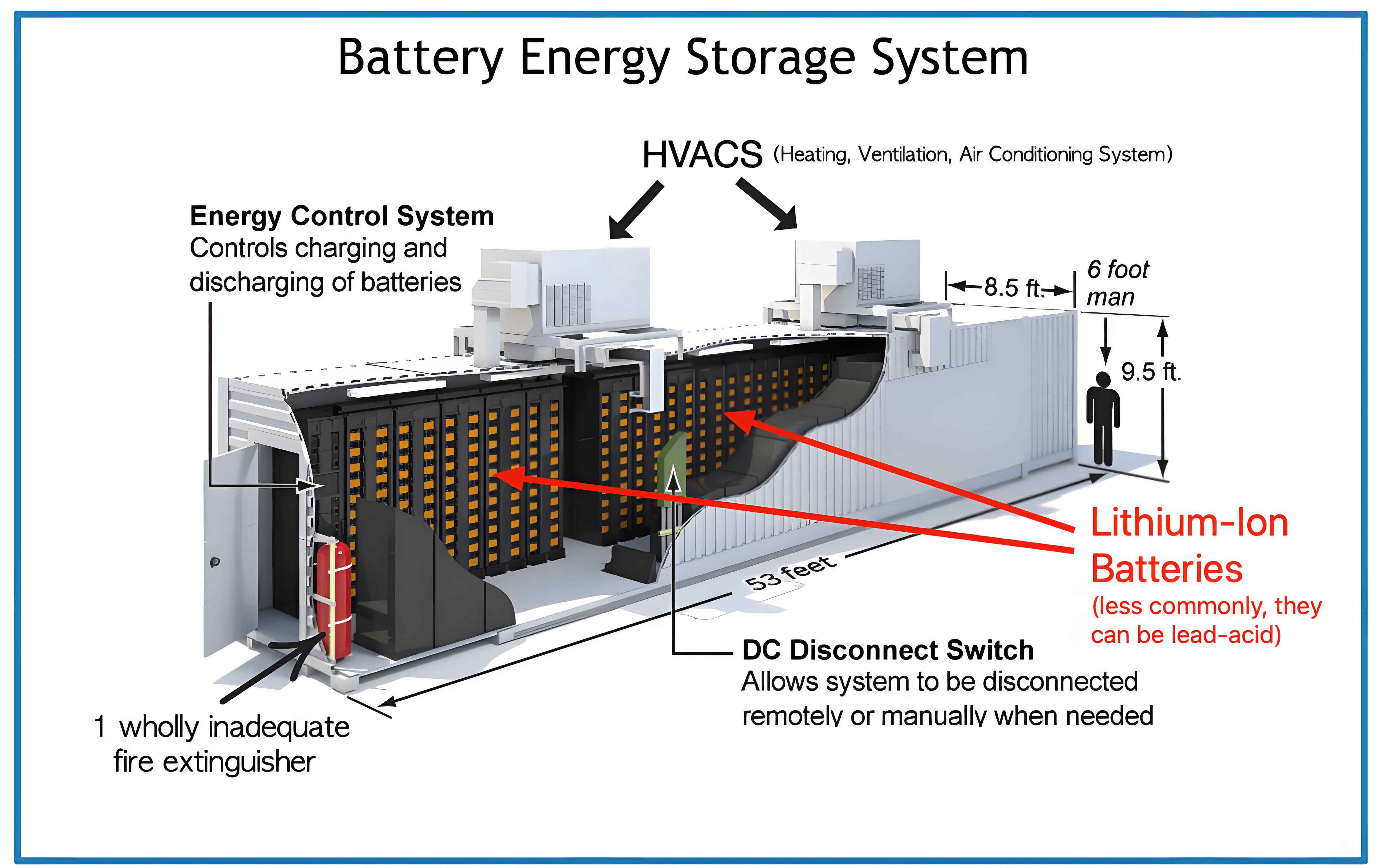
A typical configuration of the energy storage system used in a DC microgrid is shown in the following figure. The DC bus is connected to the AC grid, renewable sources and loads through appropriate power electronic interfaces. The battery, which is a critical element of the energy storage system, exchanges energy with the DC bus through the bidirectional converter investigated in my work.
The bidirectional converter must satisfy several requirements: high voltage step-up and step-down capability, low current ripple, low voltage stress of the high-voltage-side switches, soft-switching operation, and galvanic isolation. Conventional bidirectional Buck/Boost converters are simple and cheap, but their voltage gain is insufficient for a 48 V-to-600 V application. Isolated converters such as the dual-active-bridge (DAB) converter offer galvanic isolation and bidirectional power transfer, but their input current ripple and the voltage stress of the high-voltage-side devices may still be problematic. Two-stage cascade converters can combine the advantages of each stage, but the current ripple and switch stress remain key challenges. In order to solve these problems, I propose a cascade topology composed of an interleaved parallel current-fed dual-active-bridge (CF-DAB) converter as the front stage and a three-level Buck/Boost converter as the rear stage. The proposed converter achieves a high overall voltage gain, low inductor current ripple, reduced switch voltage stress and soft-switching over the full operating range.
Topology of the Proposed Bidirectional DC-DC Converter
Table 1 summarizes the design specifications of the proposed converter. The low-voltage side is connected to a battery with a nominal voltage of 48 V, and the high-voltage side is connected to a DC bus rated at 600 V. The rated power is 1.2 kW and the switching frequency is 50 kHz.
| Parameter | Symbol | Value/Requirement |
|---|---|---|
| Low-side voltage range | $V_L$ | 36–60 V |
| Low-side nominal voltage | $V_L$ | 48 V |
| Clamping-capacitor voltage range | $V_{C1}$ | 115–125 V |
| Clamping-capacitor nominal voltage | $V_{C1}$ | 120 V |
| Intermediate DC-bus voltage range | $V_{dc}$ | 345–375 V |
| Intermediate DC-bus nominal voltage | $V_{dc}$ | 360 V |
| High-side voltage range | $V_H$ | 480–720 V |
| High-side nominal voltage | $V_H$ | 600 V |
| Rated output power | $P$ | 1.2 kW |
| Switching frequency | $f$ | 50 kHz |
| Inductor current ripple | – | < 20% |
| Capacitor voltage ripple | – | < 2% |
| Target efficiency | – | > 95% |
The overall topology consists of two stages. The front stage is an interleaved parallel CF-DAB converter. Compared with the conventional DAB converter, the front stage adds two interleaved inductors and a clamping capacitor on the primary side. This arrangement forms an interleaved Buck/Boost structure with the primary-side full-bridge switches, which significantly reduces the low-side current ripple and provides voltage regulation capability. The rear stage is a three-level Buck/Boost converter. By adding a voltage-divider capacitor branch, the voltage stress of each high-side switch is reduced to half of the high-side bus voltage. The cascade structure enables each stage to operate in its optimal duty-cycle range and the total voltage gain is the product of the gains of the two stages.
Analysis and Design of the Front-Stage Interleaved Parallel CF-DAB Converter
I first derive the front-stage topology from the conventional voltage-fed DAB converter. If the input source and the inductor are placed in series with the DC source, the current-fed DAB converter is obtained. The current-fed structure can limit the inrush current and reduce the current ripple, but its voltage regulation capability is poor. By replacing the single inductor with two interleaved inductors and adding a clamping capacitor across the primary side, the proposed interleaved parallel CF-DAB converter is obtained. The clamping capacitor clamps the primary-side voltage to a nearly constant value and allows the converter to operate in the voltage-matching condition.
I analyze the steady-state operation of the front-stage converter in both Boost mode and Buck mode. The primary-side switches $S_1$, $S_2$, $S_3$ and $S_4$ are controlled with pulse-width modulation. Switches $S_1$ and $S_3$ have the same duty cycle $D_1$, and the drive signal of $S_3$ is shifted by half a switching period with respect to that of $S_1$. The secondary-side switches $S_5$–$S_8$ are operated with a phase shift $\varphi$ relative to the primary-side bridge. When the phase of the primary-side AC voltage leads the secondary-side AC voltage, power flows from the low-voltage side to the intermediate bus; this is defined as the Boost mode. Conversely, when the phase is reversed, power flows in the opposite direction and the converter operates in the Buck mode.
Table 2 defines the four possible operating regions of the front-stage converter according to the duty cycle $d$ and the phase-shift angle $\varphi$.
| Operating region | Condition |
|---|---|
| Region I | $d+\varphi<1$ and $d>\varphi$ |
| Region II | $d+\varphi>1$ and $d<\varphi$ |
| Region III | $d+\varphi<1$ and $d<\varphi$ |
| Region IV | $d+\varphi>1$ and $d>\varphi$ |
The clamping-capacitor voltage of the front stage in the Boost mode can be expressed as
$$
V_{C1}=\frac{V_L}{1-D_1}.
$$
Under the voltage-matching condition, the intermediate DC-bus voltage satisfies
$$
V_{dc}=\frac{kV_{C1}}{n},
$$
where $n$ is the turns ratio of the high-frequency transformer and $k$ is the normalized voltage-transfer ratio. Combining the above equations, the voltage gain of the front stage in the Boost mode is
$$
G_{1\_Boost}=\frac{V_{dc}}{V_L}=\frac{k}{n(1-D_1)}.
$$
Similarly, the voltage gain of the front stage in the Buck mode is
$$
G_{1\_Buck}=\frac{V_L}{V_{dc}}=\frac{nD_1}{k},
$$
where $D_1$ denotes the duty cycle of the low-side switches in the step-down operation. The overall voltage gain of the cascade converter is therefore
$$
G_{Boost}=G_{1\_Boost}G_{2\_Boost}=\frac{k}{n(1-D_1)(1-D_2)},
$$
$$
G_{Buck}=G_{1\_Buck}G_{2\_Buck}=\frac{nD_1D_2}{k}.
$$
One of the most important features of the interleaved front stage is its ability to suppress the input current ripple. I derive the total current ripple of the two interleaved inductors. When the duty cycle satisfies $D_1<0.5$, the total input current ripple is
$$
\Delta i_{t\_Boost}=\frac{V_{C1}D_1(1-2D_1)}{L f},
$$
and when $D_1>0.5$, the total input current ripple is
$$
\Delta i_{t\_Boost}=\frac{V_{C1}(1-D_1)(2D_1-1)}{L f}.
$$
Compared with a single-phase Buck/Boost converter, the ratio of the current ripple of the interleaved structure to that of the single-phase structure is
$$
\alpha=
\begin{cases}
\dfrac{1-2D_1}{1-D_1}, & D_1<0.5,\\[6pt]
\dfrac{2D_1-1}{D_1}, & D_1>0.5.
\end{cases}
$$
In particular, the theoretical current ripple becomes zero when $D_1=0.5$. Therefore, by choosing a suitable operating range, the interleaved structure can greatly reduce the battery-side current ripple, which is beneficial for the lifetime of the energy storage system.
Another crucial feature is soft-switching. I analyze the zero-voltage-switching (ZVS) conditions for all switches in the front-stage converter. The ZVS conditions are summarized in Table 3, where $i_{Lk}$ is the auxiliary-inductor current and $i_p/i_v$ are the peak/valley values of the interleaved inductor currents.
| Mode | $S_1,S_3$ | $S_2,S_4$ | $S_5,S_7$ | $S_6,S_8$ |
|---|---|---|---|---|
| Boost | $i_p+i_{Lk}(t_0)>0$ | $i_v-i_{Lk}(t_1)<0$ | $ni_{Lk}(t_2)>0$ | $ni_{Lk}(t_6)>0$ |
| Buck | $i_v-i_{Lk}(t_0)<0$ | $i_p+i_{Lk}(t_1)>0$ | $ni_{Lk}(t_3)>0$ | $ni_{Lk}(t_7)>0$ |
After substituting the steady-state expressions of the inductor currents, I verify that the secondary-side switches always satisfy the ZVS conditions. In the Boost mode, $S_2$ and $S_4$ have ZVS over the full range; in the Buck mode, $S_1$ and $S_3$ have ZVS over the full range. Hence the proposed front-stage converter is able to achieve soft-switching over the complete operating range when it operates at the voltage-matching point. This reduces the switching loss and improves the system efficiency.
Based on the above analysis, I design the key parameters of the front-stage converter. The transformer turns ratio is determined by $n=V_{C1}/V_{dc}=120/360=1/3$. The auxiliary inductance $L_k$ is selected as 15 μH. The two interleaved inductors $L_1=L_2=300$ μH. The clamping capacitor is chosen as $C_1=100$ μF. The main devices are listed in Table 4.
| Component | Selected value/type |
|---|---|
| Transformer turns ratio | $n=1:3$ |
| Auxiliary inductor $L_k$ | 15 μH, EE42 core |
| Interleaved inductors $L_1,L_2$ | 300 μH |
| Clamping capacitor $C_1$ | 100 μF |
| Low-side switches $S_1$–$S_4$ | IRFP4137PBF MOSFET, 300 V/38 A |
| High-side switches $S_5$–$S_8$ | STW20NM60 MOSFET, 600 V/20 A |
Analysis and Design of the Rear-Stage Three-Level Buck/Boost Converter
The rear stage of the proposed bidirectional converter is a three-level Buck/Boost converter. Compared with the conventional two-level Buck/Boost converter, the three-level topology adds one extra voltage-divider capacitor. In the Boost mode, switches $Q_2$ and $Q_3$ are the main switches, while $Q_1$ and $Q_4$ serve as synchronous rectifiers. In the Buck mode, the roles are reversed. The phase difference between the drive signals of $Q_2$ and $Q_3$ is 180°, so the inductor voltage and the inductor current ripple have twice the switching frequency. The voltage gain of the three-level converter is the same as that of a conventional Buck/Boost converter:
$$
G_{2\_Boost}=\frac{1}{1-D_2},
$$
$$
G_{2\_Buck}=D_2′,
$$
where $D_2$ is the duty cycle in the Boost mode and $D_2’$ is the duty cycle in the Buck mode. The total voltage gain of the whole bidirectional converter is the product of the front-stage gain and the rear-stage gain. A significant advantage of the three-level structure is that the voltage stress of each switch is reduced to half of the high-side voltage. Since the high-side bus voltage reaches 600 V, the switch voltage stress is only 300 V, which allows the use of 600 V class MOSFETs with sufficient margin.
I further analyze the midpoint voltage imbalance problem of the three-level converter. In an ideal case, the two voltage-divider capacitors $C_2$ and $C_3$ share the high-side voltage equally. However, the gate-drive circuits inevitably introduce propagation delays. If the rising-edge delay $t_{LH}$ and the falling-edge delay $t_{HL}$ are not equal, the actual duty cycles of the main switches will be slightly different. This causes the charging and discharging times of the two capacitors to be unequal, and the midpoint voltage drifts from its balanced value. The voltage deviation in one switching cycle can be expressed as
$$
\Delta V=\frac{i_o\Delta t}{C},
$$
where $i_o$ is the midpoint current and $\Delta t$ is the difference between the actual conduction times of the two main switches. If no balancing action is taken, this deviation accumulates and may cause over-voltage of one switch and increased output ripple. Therefore, a midpoint voltage balancing control is required in the design.
Table 5 gives the design parameters of the rear-stage converter.
| Component | Selected value/type |
|---|---|
| Inductor $L_3$ | 1 mH |
| Voltage-divider capacitors $C_2,C_3$ | 470 μF |
| DC-bus capacitor $C_{dc}$ | 1200 μF |
| Switches $Q_1$–$Q_4$ | STW20NM60 MOSFET, 600 V/20 A |
Control Strategy and Small-Signal Modelling
The control system of the proposed bidirectional converter is divided into two independent parts. The front-stage converter is controlled by a composite PWM plus phase-shift strategy. The duty cycle $D_1$ of the low-side switches is regulated by a voltage loop to keep the clamping-capacitor voltage $V_{C1}$ at the reference value, so that the ratio between $V_{C1}$ and the intermediate bus voltage $V_{dc}$ is equal to the transformer turns ratio. The phase-shift angle $\varphi$ is regulated by another voltage loop to stabilize $V_{dc}$. The rear-stage converter uses a voltage and current double closed-loop control strategy. The outer voltage loop regulates the high-side voltage $V_H$, and the inner current loop regulates the inductor current $i_{L3}$. In addition, a duty-cycle-offset method is used to balance the midpoint voltage of the three-level converter.
I use the state-space averaging method to build the small-signal models. Because the front-stage converter has a special structure, I adopt an equivalent-splitting modelling method. The interleaved parallel CF-DAB converter is split into an interleaved Buck/Boost converter and a DAB converter. This simplification not only reduces the complexity of modelling but also facilitates the implementation of the control loops. For the interleaved Boost converter, the duty-cycle-to-inductor-current transfer function and the duty-cycle-to-output-voltage transfer function are obtained. With the derived transfer functions, I design the PI regulators using the frequency-response method. The control parameters are listed in Table 6.
| Control loop | Proportional gain | Integral gain |
|---|---|---|
| Front-stage current loop | $k_{Pi}=0.035$ | $k_{Ii}=988.153$ |
| Front-stage voltage loop | $k_{Pv}=0.0339$ | $k_{Iv}=400.433$ |
| Front-stage phase-shift loop | $k_{P\varphi}=0.727$ | $k_{I\varphi}=577.008$ |
| Rear-stage current loop | $k_{Pi}=0.436$ | $k_{Ii}=1264.122$ |
| Rear-stage voltage loop | $k_{Pv}=0.597$ | $k_{Iv}=32.819$ |
The PI controller of the current loop is represented by
$$
G_{PI,i}(s)=k_{Pi}+\frac{k_{Ii}}{s}.
$$
The PI controller of the voltage loop is represented by
$$
G_{PI,v}(s)=k_{Pv}+\frac{k_{Iv}}{s}.
$$
After compensation, the current loop has a cutoff frequency of about $4.27\times10^4$ rad/s with a phase margin of about 86°, and the voltage loop has a cutoff frequency of about $3.72\times10^3$ rad/s with a phase margin of about 85°. These margins satisfy the stability requirements and provide good dynamic performance.
For the rear-stage converter, the midpoint balancing controller uses the voltage difference between $C_2$ and $C_3$ as the feedback signal. The PI controller generates a correction term $\Delta D_2$. When $V_{C3}>V_{C2}$, the correction term is added to the duty cycle of $Q_2$ and subtracted from the duty cycle of $Q_3$. Consequently, the charging time of $C_2$ becomes longer and that of $C_3$ becomes shorter, which forces the midpoint voltage back to the balanced state.
Simulation Results
I build a simulation model in Matlab/Simulink to verify the theoretical analysis and the control strategy. The simulation parameters are the same as those listed in Table 1. In the forward operating mode, the battery-side voltage is 48 V, the intermediate DC-bus voltage is regulated at 360 V, and the high-side voltage is regulated at 600 V. The simulation results show that the front-stage converter achieves ZVS: before the gate-drive signal arrives, the drain-source voltage has already decreased to zero. Figure 4-18 in my original work demonstrates this. The transformer primary and secondary AC voltages are three-level square waves, and their phase difference changes with the transmitted power. At the rated power of 1.2 kW, the phase difference is about 1.9 μs. I also compare the proposed PWM plus phase-shift control with the conventional phase-shift control. Under the conventional phase-shift control, the transformer primary voltage cannot maintain the voltage-matching condition, and the auxiliary-inductor current contains evident current spikes. Under the proposed control, the converter works at the voltage-matching point, and the current spikes are effectively suppressed.
The simulated waveforms of the two interleaved inductor currents show that the total input current ripple is only about 2 A, which is much lower than the ripple of each individual inductor current. The clamping-capacitor voltage is regulated at 120 V with a voltage ripple of about 0.1 V. The intermediate DC-bus voltage is regulated at 360 V with a ripple of about 0.4 V. When the low-side voltage steps from 48 V to 60 V, the DC-bus voltage recovers to 360 V within about 15 ms, which verifies the dynamic regulation capability of the front-stage converter.
For the rear-stage converter, the inductor current $i_{L3}$ is stable at about 3.3 A and its ripple is about 0.6 A. The voltage waveforms of the inductor and the midpoint of the bridge legs are complementary, which is consistent with the theoretical analysis. The midpoint voltage balancing control is tested by enabling the balancing loop at 0.1 s. Before the balancing loop is enabled, the voltages of the two dividing capacitors are significantly different. After enabling, the two capacitor voltages converge to the same value of 300 V within about 4 ms in the forward mode and about 2 ms in the reverse mode. The high-side output voltage maintains a stable value of 600 V. When a load step is applied, the output voltage recovers quickly, confirming a good dynamic response.
The simulation is also carried out in the reverse operating mode, where energy flows from the high-voltage side to the battery side. The rear-stage converter operates as a Buck converter and regulates the intermediate DC-bus voltage at 360 V. The front-stage converter operates as a DAB converter in the Buck mode and regulates the low-side voltage at 48 V. The simulation results show that the proposed converter can achieve bidirectional power transfer smoothly. Figure 4-30 in my original model demonstrates the ZVS of the secondary-side switches in the reverse mode. The interleaved inductors still provide a low current ripple. Table 7 summarizes the simulated ripple values in both operating modes.
| Quantity | Forward mode | Reverse mode |
|---|---|---|
| $V_{C1}$ voltage ripple | 0.1 V | 0.1 V |
| $V_{dc}$ voltage ripple | 0.4 V | – |
| $V_H$ voltage ripple | < 1% | – |
| Input current ripple (48 V side) | 2 A | 1.5 A |
| Rear-stage inductor current ripple | 0.6 A | 0.6 A |
Hardware Design and Experimental Verification
To further verify the validity of the proposed design, I construct a 1.2 kW experimental prototype. The control algorithm is implemented on a TMS320F28335 digital signal processor. The hardware system includes the main power circuit, isolated gate-drive circuits, voltage and current sampling circuits, and an auxiliary power supply. The gate-drive circuit uses the UCC21520 isolated driver, which provides a maximum 4 A source current and 6 A sink current. The driving voltage is +15 V/-3.5 V, which ensures reliable turn-on and fast turn-off of the MOSFETs. The voltage sampling circuit uses an AMC1200 isolated amplifier and an SGM8631 operational amplifier. The current sampling circuit uses a CC6920BSO Hall-effect current sensor with a range of 0–30 A.
The software program includes a main program and an interrupt service subroutine. The main program initializes the system clock, GPIO, ADC and EPWM modules. In the interrupt service routine, the sampled voltages and currents are read, and the over-voltage and over-current protections are checked. If the values are within the safe range, the control loops are executed and the PWM duty cycles are updated. The midpoint balancing control is also embedded in the interrupt service subroutine.
I test the prototype in both forward and reverse modes. In the forward mode, the experimental waveforms show that the drain-source voltage of the low-side MOSFET $S_1$ drops to zero before its gate source voltage rises, which confirms the ZVS operation. The two interleaved inductor currents have a ripple of about 4.8 A each, but the total input current ripple is only about 2.4 A. The transformer primary and secondary voltages are three-level square waves. At full load, the phase difference is about 1.9 μs, and at half load, the phase difference is about 1 μs. This agrees well with the simulation results. The clamping-capacitor voltage is regulated at 120 V and the intermediate DC-bus voltage is regulated at 360 V. The rear-stage inductor current ripple is about 0.6 A. The voltages of the two dividing capacitors are balanced at 300 V, and the high-side output voltage is stable at 600 V.
In the reverse mode, the energy flows from the high-voltage side to the low-voltage side. The inductor current direction changes accordingly. The three-level Buck/Boost converter regulates the intermediate DC-bus voltage, and the front-stage converter regulates the low-side voltage at 48 V. The secondary-side switch $S_5$ achieves ZVS. The interleaved inductors still suppress the total current ripple effectively. The experimental results verify that the bidirectional converter can operate correctly in both directions.
I also measure the efficiency of the prototype. Table 8 lists the measured efficiency at different power levels. The proposed converter achieves its peak efficiency at approximately 1 kW. At the rated power of 1.2 kW, the forward step-up efficiency is 95.43% and the reverse step-down efficiency is 95.21%. Both values are above 95%, which meets the design target.
| Output power (kW) | Forward efficiency (%) | Reverse efficiency (%) |
|---|---|---|
| 0.2 | 93.10 | 94.02 |
| 0.4 | 94.25 | 94.78 |
| 0.6 | 94.88 | 95.03 |
| 0.8 | 95.12 | 95.15 |
| 1.0 | 95.39 | 95.28 |
| 1.2 | 95.43 | 95.21 |
Conclusion
In this thesis, I have proposed a high-gain bidirectional DC-DC converter for the energy storage system in a DC microgrid. The converter consists of an interleaved parallel CF-DAB front stage and a three-level Buck/Boost rear stage. Through detailed theoretical analysis, small-signal modelling, simulation and experimental verification, the following conclusions are drawn:
First, the interleaved parallel structure in the front stage effectively reduces the current ripple on the battery side, which is beneficial to the lifetime and thermal performance of the energy storage system. The composite PWM plus phase-shift control enables the front-stage converter to operate under the voltage-matching condition, suppresses the current spike in the auxiliary inductor, and achieves ZVS for all switches over the full operating range.
Second, the three-level Buck/Boost rear stage halves the voltage stress of the high-side switches. The duty-cycle-offset midpoint balancing control successfully maintains the balance of the two dividing-capacitor voltages, and the double closed-loop control provides excellent steady-state and dynamic performance.
Third, the overall voltage gain of the cascade topology is the product of the two stage gains, and the converter can realize 48 V-to-600 V bidirectional power conversion with a rated power of 1.2 kW and an efficiency above 95%. The simulation and experimental waveforms confirm the correctness of the topology analysis and the effectiveness of the control strategy.
In future work, I plan to further improve the power density by integrating the magnetic components and to develop an intelligent algorithm for automatic switching between the forward and reverse operating modes, which will make the converter more suitable for practical energy storage system applications.