
In the rapid expansion of renewable energy generation, the solar inverter plays a pivotal role as the core interface between photovoltaic (PV) arrays and the utility grid. The quality of power injected into the grid heavily depends on the control performance of the solar inverter. Among numerous challenges, the dead‑zone effect inherent in switching devices, parameter uncertainties, and external disturbances are the primary factors that degrade the output waveform quality. In my research, I propose an integral sliding mode control strategy specifically designed for a solar inverter system that explicitly accounts for the dead‑zone effect. This approach not only mitigates the adverse impacts of dead‑zone but also enhances robustness against model mismatches and external perturbations.
I begin by thoroughly analyzing the mechanism of dead‑zone in a three‑phase voltage‑source solar inverter. The dead‑zone time introduced intentionally to prevent shoot‑through faults, combined with the turn‑on and turn‑off delays of power switches, creates a deviation between the ideal switching signal and the actual one. This deviation results in a voltage error that depends on the direction of the phase current. For a typical solar inverter, such an error leads to increased total harmonic distortion (THD) and reduced efficiency. To capture this effect mathematically, I employ the state‑space averaging method and derive an equivalent model that includes the dead‑zone distortion voltage. The average output voltage of phase A over one switching cycle is expressed as:
$$
\langle U_{AN} \rangle_{T_s} = \frac{U_{dc}}{2U_{tri}} \left( U_m – \text{sgn}(i_A) U_{dc} D’ \right)
$$
where \(U_{dc}\) is the DC‑link voltage, \(U_m\) the modulation wave amplitude, \(U_{tri}\) the carrier amplitude, and \(D’\) represents the duty‑cycle variation caused by dead‑zone and switching delays. The term \(-\text{sgn}(i_A)U_{dc}D’\) is exactly the dead‑zone distortion voltage \(\Delta U_{DT}\). Similar expressions hold for phases B and C.
Based on this analysis, I construct a complete mathematical model of the solar inverter system considering dead‑zone, parameter uncertainties, and external disturbances. The system is described by a set of differential equations in the stationary abc frame. After applying Kirchhoff’s laws, the state‑space representation is obtained as:
$$
\begin{aligned}
L_s \frac{di_K}{dt} &= U_{dc}\left(S_K – \frac{1}{3}\sum_{K=A,B,C} S_K\right) + \Delta U_K – (R_L+R_S)i_K – U_{gK} \\
L_g \frac{di_{gK}}{dt} &= -R_g i_{gK} – U_{gK} + U_C \\
C \frac{dU_C}{dt} &= i_K – i_{gK} + R_C C\left(\frac{di_K}{dt} – \frac{di_{gK}}{dt}\right)
\end{aligned}
$$
with
$$
\Delta U_K = \frac{t_d + t_{on} – t_{off}}{3T_s} \sum_{K=A,B,C} \text{sgn}(i_K) + \Delta U_{DT}
$$
I further define the state vector \(\mathbf{x} = [i_K,\; i_{gK},\; U_C]^T\) and lump all uncertainties and disturbances into a composite disturbance \(d\). The resulting linear‑like form is:
$$
\dot{\mathbf{x}} = A\mathbf{x} + B\mathbf{u} + \mathbf{G}, \qquad y = F\mathbf{x}
$$
where matrices \(A\), \(B\), \(F\) and the input vector \(\mathbf{u}\) are given explicitly in the paper. This model serves as the foundation for all subsequent controller design.
To effectively estimate the composite disturbance \(d\) and the system states, I design a proportional‑integral type disturbance state observer. The observer structure is depicted conceptually in the conventional observer block diagram. The observer dynamics are:
$$
\dot{\hat{\mathbf{x}}} = A\hat{\mathbf{x}} + B\mathbf{u} + \hat{\mathbf{G}} + M\tilde{\mathbf{x}}, \qquad \hat{y} = F\hat{\mathbf{x}}
$$
where \(\tilde{\mathbf{x}} = \mathbf{x} – \hat{\mathbf{x}}\) is the estimation error, and \(\hat{\mathbf{G}} = [0,0,\hat{d}]^T\). The observation error dynamics become:
$$
\dot{\tilde{\mathbf{x}}} = (A – M)\tilde{\mathbf{x}} + (d – \hat{d})
$$
I prove that by choosing \(M\) and the gain matrices \(L_1, L_2\) in the disturbance estimator
$$
\hat{d} = L_1 H + \int_0^t L_2 H d\tau + \hat{d}(0)
$$
the estimation error system is asymptotically stable in the sense of Lyapunov. The key condition is that the transfer function \(G(s) = E[sI-(A-M)]^{-1}\) must be strictly positive real, and the integral inequality \(\zeta(0,t) \ge -\gamma^2\) holds.
With the estimated states and disturbance, I proceed to design a non‑singular terminal sliding mode controller for the solar inverter. Let the tracking errors be:
$$
\sigma_1 = i_K^{ref} – i_K, \quad \sigma_2 = i_{gK}^{ref} – i_{gK}, \quad \sigma_3 = U_C^{ref} – U_C
$$
Define the auxiliary variables:
$$
J_1 = \theta_1 \sigma + \theta_2 \int_0^t \sigma d\tau, \quad J_2 = \dot{J}_1 = \theta_1 \dot{\sigma} + \theta_2 \sigma
$$
where \(\theta_1, \theta_2 > 0\). The sliding surface is chosen as:
$$
\mathbf{z} = J_1 + \delta J_2^{p/q}
$$
with \(1 < p/q < 2\), \(\delta = \text{diag}(\delta_1,\delta_2)\), and \(p,q\) odd. The control law is derived as:
$$
\mathbf{e} = \frac{1}{b}\left( \mathbf{e}_1 – \mathbf{e}_2 + \hat{d} \right)
$$
$$
\mathbf{e}_1 = A\mathbf{x} – \frac{\theta_2}{\theta_1}\sigma
$$
$$
\mathbf{e}_2 = \int_0^t \left[ k_1 \text{sgn}(s) + \frac{q}{\theta_1 p} \delta^{-1} J_2^{1-p/q} + k_2 \mathbf{z} \right] d\tau
$$
I prove the closed‑loop stability using a Lyapunov function \(V = \frac{1}{2}\mathbf{z}^T \mathbf{z}\). Its derivative satisfies:
$$
\dot{V} \le -\frac{\theta_1 p}{q} \min_i \{\delta_i J_{2i}^{p/q-1}\} \left( k_1 \|\mathbf{z}\| + k_2 \|\mathbf{z}\|^2 \right) \le 0
$$
Thus the system state will reach the sliding surface in finite time and maintain on it, achieving zero steady‑state error. To alleviate chattering, I replace the sign function with a saturation function \(\text{sat}(s/\alpha)\).
I carried out extensive simulations using PSIM to validate the proposed strategy. The parameters of the solar inverter system are listed in Table 1.
| Parameter | Symbol | Value |
|---|---|---|
| DC input voltage | \(U_{in}\) | 360 V |
| Output AC voltage (RMS) | \(U_{out}\) | 220 V |
| Switching frequency | \(f_s\) | 10 kHz |
| Rated load resistance | \(R_{load}\) | 44 \(\Omega\) |
| Output filter inductance | \(L_s\) | 4 ± 2 mH |
| Output filter capacitance | \(C\) | 28.2 ± 13 \(\mu\)F |
| Controller gain \(\theta_1\) | – | 12 |
| Controller gain \(\theta_2\) | – | 12 |
| Sliding surface exponent \(p\) | – | 13 |
| Sliding surface exponent \(q\) | – | 11 |
| \(\delta_1, \delta_2\) | – | 0.001 |
| \(k_1\) | – | 100 |
| \(k_2\) | – | 8×10³ |
First, I tested the solar inverter under rated load startup. The output voltage and current waveforms settle within one fundamental cycle with negligible overshoot. The THD of the voltage is as low as 0.024%, indicating excellent power quality.
Second, I examined load disturbance scenarios. The load resistance was stepped from 34 \(\Omega\) to 15 \(\Omega\) at \(t=0.1\) s and then back to 34 \(\Omega\) at \(t=0.2\) s. For a linear resistive load, the output voltage remains almost unchanged (THD = 0.025%). For a nonlinear load (single‑phase diode rectifier), the voltage amplitude stays at 220 V with THD = 0.034%. These results demonstrate the strong disturbance rejection capability of the proposed controller for the solar inverter.
Third, I intentionally introduced dead‑zone and switching delays into the simulation. Initially, the output voltage amplitude dropped to about 210 V due to dead‑zone; however, within 0.005 s the controller compensated the distortion and the voltage recovered to the ideal 220 V. This confirms that modeling the dead‑zone effect in the solar inverter and incorporating it into the observer design effectively mitigates its negative impact.
Fourth, I varied the DC‑link voltage from 360 V to 380 V and back. Despite this severe perturbation, the solar inverter output remains nearly unaffected. The proposed strategy relaxes the requirement for a large DC‑side capacitor, reducing the weight and volume of the system.
To further quantify the performance, I summarize the key simulation results in Table 2.
| Test Scenario | Condition | Voltage THD (%) | Response Time (ms) |
|---|---|---|---|
| Rated startup | Linear load, 44 \(\Omega\) | 0.024 | < 20 |
| Load step (linear) | 34 \(\Omega\) → 15 \(\Omega\) → 34 \(\Omega\) | 0.025 | < 1 |
| Load step (nonlinear) | Diode rectifier | 0.034 | < 2 |
| Dead‑zone compensation | \(t_d = 5~\mu\)s | 0.030 (after compensation) | 5 |
| DC voltage variation | 360 V → 380 V → 360 V | < 0.03 | < 1 |
In summary, the proposed integral sliding mode control integrated with a disturbance state observer provides a comprehensive solution for high‑performance solar inverter operation. It effectively handles dead‑zone induced voltage errors, parameter uncertainties, and external disturbances. The control law ensures fast dynamic response, zero steady‑state error, and low harmonic distortion. The simulation results strongly support the theoretical analysis and demonstrate the superiority of the method compared to conventional PI or repetitive control approaches.
The successful application of this strategy to a solar inverter highlights its potential in real‑world photovoltaic systems where reliability and power quality are paramount. Future work will focus on experimental validation and extension to multi‑level solar inverter topologies.
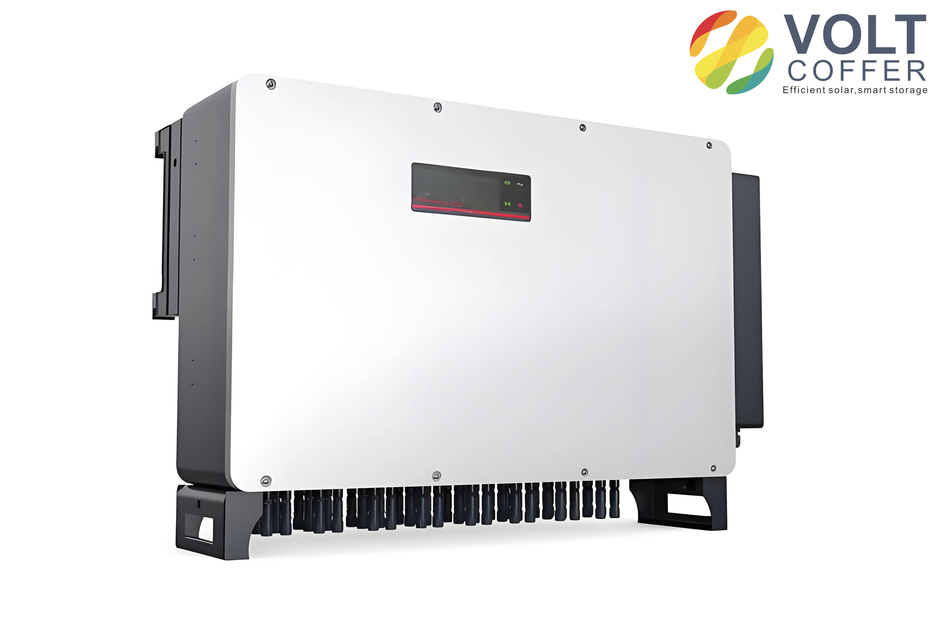
This photo illustrates a typical outdoor solar inverter installation. The robust enclosure protects the power electronics, including the IGBT modules that are subject to dead‑zone effects. The control algorithm presented in this paper can be directly implemented in the digital signal processor (DSP) inside such a solar inverter to achieve superior performance.
Finally, I emphasize that the repeated mention of “solar inverter” throughout this article reflects the central role that this device plays in the proposed control design. Every mathematical model, observer, and controller is tailored specifically for the solar inverter context. The dead‑zone effect, often neglected in generic inverter studies, becomes a critical factor that must be addressed to meet stringent grid‑connection standards. By explicitly including it in the system dynamics, my approach provides a more accurate representation of the real solar inverter operation and leads to a more effective control solution.