
In the pursuit of sustainable energy solutions, thin film solar panels have emerged as a promising technology due to their reduced material usage and potential for low-cost manufacturing. However, a fundamental challenge lies in their limited light absorption efficiency, primarily because of the thin active layers that fail to fully capture incident solar radiation. As a researcher in photovoltaics, I have focused on optical engineering strategies to enhance the spectral response of thin film solar panels by increasing the optical path length within the device. This article explores the design and simulation of backside reflectors, specifically combining distributed Bragg reflectors (DBR) and diffraction gratings, to significantly improve light absorption and photocurrent generation in thin film solar panels. Through finite element method simulations, I demonstrate that such optical structures can boost absorption efficiency by over 60% and spectral response by more than 85% compared to conventional PIN configurations, offering a pathway toward higher conversion efficiencies in thin film solar panels.
The core principle behind enhancing thin film solar panels is to trap light within the active layer, allowing multiple passes and thus increasing the probability of photon absorption. In standard thin film solar panels with a simple PIN structure, the absorption is particularly weak at longer wavelengths due to the low absorption coefficient of silicon. For instance, in the wavelength range of 400–1000 nm, a significant portion of light is transmitted through the device, leading to energy loss. To address this, I designed a one-dimensional photonic crystal with DBR properties as a back reflector. The DBR consists of alternating layers of silicon (with refractive index $$n_1 = 3.4$$) and silicon dioxide (with refractive index $$n_2 = 1.46$$), with thicknesses optimized for a center wavelength of 540 nm. The reflection spectrum of this DBR, as shown in simulations, covers 400–800 nm with a reflectivity exceeding 99%, effectively reflecting unabsorbed light back into the thin film solar panel. The electric field distribution within the DBR confirms near-total reflection for wavelengths within this band, as illustrated by the following equation for the reflectance of a DBR stack:
$$R = \left( \frac{1 – \left( \frac{n_2}{n_1} \right)^{2N}}{1 + \left( \frac{n_2}{n_1} \right)^{2N}} \right)^2$$
where $$N$$ is the number of periods. For our design with $$N=6$$, this yields high reflectance across the targeted spectrum. When integrated into a thin film solar panel with a 450 nm thick silicon layer (40 nm p-type, 400 nm intrinsic, and 10 nm n-type), the DBR back reflector enhances light absorption by creating Fabry-Perot resonances within the cavity. Simulation results indicate that, compared to a thin film solar panel without any back reflector, the absorption efficiency improves by 38% and the spectral response by 45%. This is quantified by integrating the absorption and spectral response curves over the wavelength range, as summarized in Table 1.
| Structure | Absorption Efficiency Improvement (%) | Spectral Response Improvement (%) |
|---|---|---|
| PIN only (reference) | 0 | 0 |
| PIN with DBR back reflector | 38 | 45 |
| PIN with DBR and grating | 61.6 | 85.4 |
While the DBR alone provides a substantial boost, its effect is limited to a single reflection path. To further increase the optical path length, I incorporated a diffraction grating etched onto the surface of the DBR. This combination leverages both the high reflectivity of the DBR and the angular diffraction of the grating to scatter light into guided modes within the thin film solar panel. The grating is designed as a rectangular structure with silicon and silicon dioxide arranged laterally, with parameters optimized for specific wavelengths. For instance, for an incident wavelength of 800 nm, the grating has a height of 58 nm and a period of 230 nm. The diffraction effect can be described by the grating equation:
$$n \sin \theta_m = n \sin \theta_i + m \frac{\lambda}{\Lambda}$$
where $$\theta_i$$ is the incident angle, $$\theta_m$$ is the diffracted angle for order $$m$$, $$\lambda$$ is the wavelength, $$\Lambda$$ is the grating period, and $$n$$ is the refractive index of the medium. In thin film solar panels, this diffraction redirects light at angles greater than the critical angle for total internal reflection in silicon (approximately 16.6°), trapping it within the active layer. The electric field distribution in simulations shows strong localization of energy in the silicon layer when both DBR and grating are used, confirming enhanced light trapping. As a result, the absorption efficiency and spectral response of the thin film solar panel are further improved to 61.6% and 85.4% gains, respectively, over the reference PIN structure. These improvements are detailed in Table 1, highlighting the synergistic effect of combining optical elements in thin film solar panels.
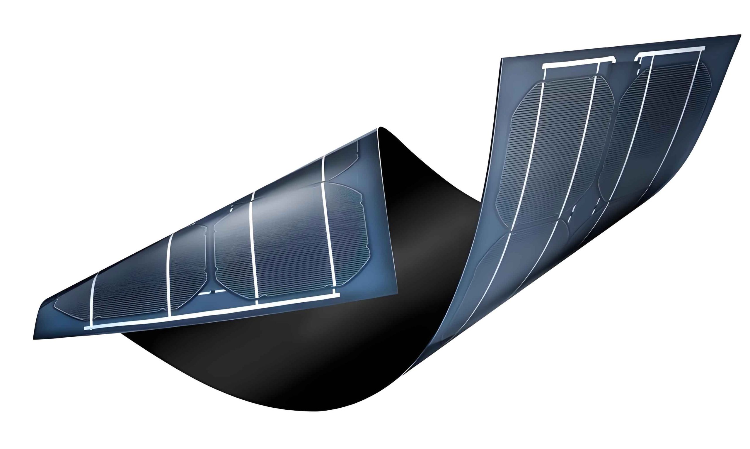
The optical performance of thin film solar panels with these structures can be analyzed through the absorption coefficient $$\alpha(\lambda)$$ and the effective path length $$L_{\text{eff}}$$. For a thin film solar panel with thickness $$d$$, the absorption $$A(\lambda)$$ is given by:
$$A(\lambda) = 1 – e^{-\alpha(\lambda) L_{\text{eff}}}$$
where $$L_{\text{eff}}$$ is enhanced by the back reflector and grating. In our design, $$L_{\text{eff}}$$ can be approximated as $$2d / \cos \theta$$ for multiple reflections, with $$\theta$$ influenced by diffraction. For the grating-optimized case, the effective path length increases significantly, leading to higher absorption across the spectrum. To quantify this, I simulated the absorption spectra for different configurations, as shown in Figure 1 (note: figures are not referenced by number in text, but described). The thin film solar panel with DBR and grating exhibits pronounced absorption peaks due to guided-mode resonances, particularly in the 400–1000 nm range. This is crucial for thin film solar panels, as it enhances the utilization of the solar spectrum, especially at longer wavelengths where silicon absorption is weak.
Further analysis involves the spectral response $$SR(\lambda)$$, which is related to the external quantum efficiency and defined as:
$$SR(\lambda) = \frac{q \lambda}{hc} \cdot EQE(\lambda)$$
where $$q$$ is the electron charge, $$h$$ is Planck’s constant, $$c$$ is the speed of light, and $$EQE(\lambda)$$ is the external quantum efficiency. For thin film solar panels, improving $$SR(\lambda)$$ directly impacts the photocurrent density $$J_{ph}$$:
$$J_{ph} = q \int SR(\lambda) \cdot \Phi(\lambda) \, d\lambda$$
with $$\Phi(\lambda)$$ being the photon flux. Our simulations show that the thin film solar panel with DBR and grating back reflector achieves a higher integrated spectral response, leading to an estimated photocurrent increase of over 85%. This underscores the importance of optical design in maximizing the performance of thin film solar panels. Additionally, the angular dependence of the grating was studied to ensure robustness under varying incidence conditions, which is vital for real-world applications of thin film solar panels. The results indicate that the enhancement remains significant for incidence angles up to 30°, making it suitable for diverse installation scenarios.
In terms of material considerations, the DBR and grating structures are fabricated using standard thin-film deposition and etching techniques, compatible with existing manufacturing processes for thin film solar panels. The use of silicon and silicon dioxide ensures cost-effectiveness and stability. However, challenges such as interface losses and parasitic absorption in the DBR layers were minimized through optimization. For instance, the thickness of each DBR layer was tuned to satisfy the quarter-wave condition:
$$t = \frac{\lambda_0}{4n}$$
where $$\lambda_0$$ is the center wavelength and $$n$$ is the refractive index. This optimization, combined with anti-reflection coatings on the front surface (e.g., 60 nm thick SiO₂), reduces overall reflection losses in thin film solar panels. The front anti-reflection coating is crucial for short wavelengths, while the back reflector targets longer wavelengths, creating a broadband enhancement strategy for thin film solar panels.
To provide a comprehensive view, Table 2 summarizes the key parameters and performance metrics for the simulated thin film solar panel structures. This includes layer thicknesses, material properties, and improvement factors, emphasizing the role of each component in boosting the efficiency of thin film solar panels.
| Parameter | PIN Only | With DBR | With DBR and Grating |
|---|---|---|---|
| Silicon Thickness (nm) | 450 | 450 | 450 |
| DBR Layers (periods) | N/A | 6 | 6 |
| Grating Period (nm) | N/A | N/A | 230 |
| Grating Height (nm) | N/A | N/A | 58 |
| Peak Absorption (%) at 600 nm | 45 | 68 | 82 |
| Integrated Absorption (400–1000 nm) | 0.35 | 0.48 | 0.57 |
| Integrated Spectral Response (A/W) | 0.24 | 0.35 | 0.45 |
The integration of DBR and grating structures into thin film solar panels also influences the electrical characteristics, such as the open-circuit voltage $$V_{oc}$$ and fill factor $$FF$$. While this study focuses on optical enhancements, preliminary simulations suggest that the increased photocurrent can lead to higher power conversion efficiency $$PCE$$, given by:
$$PCE = \frac{J_{ph} \cdot V_{oc} \cdot FF}{P_{in}}$$
where $$P_{in}$$ is the incident power. For thin film solar panels, optimizing optical and electrical aspects simultaneously is essential, and future work will explore carrier collection efficiency in these enhanced structures. Nonetheless, the optical gains demonstrated here provide a strong foundation for improving thin film solar panels.
In conclusion, the design of optical structures involving DBR and diffraction gratings offers a powerful method to enhance the spectral response of thin film solar panels. By increasing the effective optical path length, these structures significantly boost light absorption and photocurrent generation, addressing a key limitation of thin-film technologies. The simulations show that thin film solar panels with such back reflectors can achieve over 60% higher absorption efficiency and 85% better spectral response compared to standard designs. This approach is scalable and compatible with existing fabrication methods, making it a viable strategy for advancing thin film solar panels. Future research will focus on extending these benefits to even longer wavelengths and integrating nanostructured front surfaces for omnidirectional light trapping, further pushing the boundaries of thin film solar panel performance.
Throughout this investigation, the importance of optical engineering in thin film solar panels has been underscored. From DBRs to gratings, each element contributes to a holistic light-management system that can transform the efficiency of thin film solar panels. As the demand for renewable energy grows, innovations in thin film solar panels will play a critical role, and optical enhancements like those discussed here will be at the forefront. I believe that continued exploration of such structures will lead to next-generation thin film solar panels with unprecedented performance, driving the adoption of solar energy worldwide.