
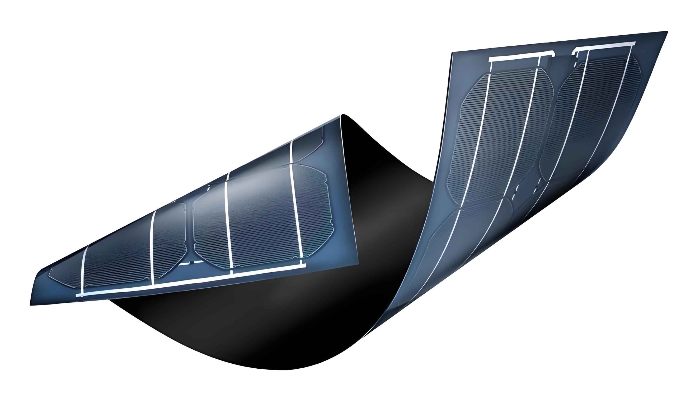
The quest for sustainable and clean energy solutions has positioned solar power at the forefront of global research initiatives. Among the various technologies, thin film solar panels offer distinct advantages in terms of material usage, flexibility, and potential for lower-cost manufacturing. A particularly intriguing class of materials for next-generation thin film solar panels are ferroelectric oxides, which exhibit a unique “bulk photovoltaic effect.” This phenomenon, arising from their non-centrosymmetric crystal structure, allows for the generation of a steady photocurrent and a photovoltage that can, in principle, exceed the material’s bandgap. This characteristic presents a significant opportunity to overcome the fundamental Shockley-Queisser efficiency limit that constrains conventional p-n junction solar cells.
Bismuth ferrite (BiFeO3, BFO) stands out as a promising candidate for ferroelectric photovoltaic applications. It is a room-temperature multiferroic material, possessing both ferroelectric and antiferromagnetic properties. More importantly for photovoltaics, BFO boasts a relatively narrow bandgap (approximately 2.1–2.6 eV), a large remnant polarization, and a high absorption coefficient in the visible spectrum. These attributes make it highly suitable for absorbing sunlight and generating electron-hole pairs. However, the practical power conversion efficiency (PCE) of BFO-based thin film solar cells has been limited by challenges such as high charge recombination rates and non-ideal interfaces with electrodes, which impede efficient charge extraction.
In this comprehensive exploration, we delve into a critical strategy for overcoming these limitations: interface engineering. The interfaces between the active light-absorbing layer and the charge-collecting electrodes are pivotal in determining the overall performance of any solar cell device. In ferroelectric thin film solar panels, these interfaces influence the built-in electric field, charge injection barriers, and carrier transport dynamics. We investigate the application of two distinct types of interfacial modification layers—an inorganic reduced graphene oxide (RGO) layer and an organic octadecyltrichlorosilane (OTS) self-assembled monolayer—to enhance the photovoltaic properties of sol-gel derived BFO thin films. Our findings reveal distinct and complementary roles for these modifiers, offering valuable insights for the rational design of high-performance ferroelectric photovoltaic devices.
1. Material Synthesis and Device Fabrication
The foundation of our study lies in the preparation of high-quality, phase-pure BFO thin films. We employed a sol-gel spin-coating technique, which is renowned for its excellent control over stoichiometry, homogeneity, and thickness. The precursor solution was formulated by dissolving bismuth nitrate pentahydrate and iron nitrate nonahydrate in a 2-methoxyethanol solvent, with acetic anhydride added as a dehydrating agent to stabilize the solution. The molar ratio of Bi:Fe was carefully adjusted to 1.05:1 to compensate for the volatility of bismuth during high-temperature annealing, ensuring the formation of a pure perovskite phase without secondary Bi2O3 or Fe2O3 phases.
A critical aspect of the film processing was the adoption of a layer-by-layer annealing protocol. Each spun-coated layer was sequentially subjected to a low-temperature bake (220°C) to evaporate solvents, a pyrolysis step (350°C) to remove organic constituents, and a final crystallization anneal at 600°C. This process was repeated ten times to build up a film thickness of approximately 700 nm. This iterative method is crucial as the crystallized layer from the previous cycle acts as a seed layer for the subsequent one, promoting highly oriented, columnar grain growth with reduced nucleation barriers and excellent crystallinity, as confirmed by structural analysis.
The fabricated BFO films were then modified with different interfacial layers to create four distinct device architectures for comparison:
- Device A (Control): FTO / BFO / Pt
- Device B (RGO-modified): FTO / BFO / RGO / Pt
- Device C (OTS-modified): FTO / BFO / OTS / Pt
- Device D (Dual-modified): FTO / BFO / OTS / RGO / Pt
The RGO layer was deposited by spin-coating a dispersion of graphene oxide (GO) onto the BFO surface, followed by thermal treatment and subsequent ultraviolet irradiation to reduce the GO to RGO. The OTS layer was formed by immersing the BFO film in a toluene solution of OTS, allowing for the self-assembly of a monolayer via silanol chemistry, followed by a thermal curing step. Finally, circular platinum (Pt) top electrodes were sputtered onto all structures through a shadow mask to complete the thin film solar panel devices for electrical characterization.
2. Structural and Morphological Characterization
X-ray diffraction (XRD) analysis confirmed the successful synthesis of pure-phase, polycrystalline BFO films belonging to the rhombohedral R3c space group. The diffraction patterns showed sharp peaks corresponding to the perovskite structure, with no detectable impurity phases such as Bi2Fe4O9 or Bi25FeO40. The introduction of the RGO or OTS interface layers did not alter the crystal structure of the underlying BFO film, as evidenced by the consistent peak positions. However, a slight attenuation in peak intensity was observed, particularly for the OTS-modified sample, which can be attributed to the increased surface coverage by the organic layer.
The cross-sectional scanning electron microscopy (SEM) images provided crucial insights into the device architecture and film quality. The BFO layer exhibited a dense, columnar microstructure with grain boundaries extending through the film thickness, which is favorable for charge transport. The measured layer thicknesses were consistent and reproducible. The RGO layer appeared as a conformal, multi-laminated sheet tightly adhered to the BFO surface. The OTS layer, formed by evaporation deposition, presented a continuous film with minor nanoscale undulations. Importantly, all interfaces (FTO/BFO, BFO/modifier, modifier/Pt) were sharp and well-defined, indicating good adhesion and no severe intermixing, which is essential for robust device operation in thin film solar panels.
The key material properties relevant to photovoltaic performance are summarized in the table below.
| Material/Layer | Primary Function | Key Property | Estimated Thickness |
|---|---|---|---|
| BiFeO3 (BFO) | Active Light Absorber | Bandgap ~2.3 eV, Ferroelectric | ~700 nm |
| Reduced Graphene Oxide (RGO) | Inorganic Interface Modifier / Hole Transport Layer | High electrical conductivity, Tunable work function | 150-200 nm |
| Octadecyltrichlorosilane (OTS) | Organic Interface Modifier / Passivation Layer | Hydrophobic, Forms self-assembled monolayer (SAM) | 50-70 nm |
| Platinum (Pt) | Top Electrode | High work function (~5.6 eV) | ~80 nm |
| Fluorine-doped Tin Oxide (FTO) | Bottom Transparent Electrode | Transparent, conductive | ~500 nm |
3. Photovoltaic Performance and Quantitative Analysis
The current density-voltage (J-V) characteristics of all devices were measured under standard AM 1.5G illumination (100 mW/cm²). The control BFO device (Device A) exhibited typical ferroelectric photovoltaic behavior with an open-circuit voltage (Voc) of 0.67 V, a short-circuit current density (Jsc) of -2.30 mA/cm², and a fill factor (FF) of 0.664, yielding a power conversion efficiency (PCE) of 1.03%. The introduction of interface modification layers led to significant and differentiated changes in these parameters.
The performance metrics for all four device architectures are systematically compared in the following table.
| Device Structure | Jsc (mA/cm²) | Voc (V) | Fill Factor (FF) | Max Power (|JV|max) (mW/cm²) | Power Conversion Efficiency (PCE) (%) |
|---|---|---|---|---|---|
| FTO / BFO / Pt (Device A) | -2.30 | 0.67 | 0.664 | 1.03 | 1.03 |
| FTO / BFO / RGO / Pt (Device B) | -2.06 | 0.84 | 0.965 | 1.67 | 1.67 |
| FTO / BFO / OTS / Pt (Device C) | -1.49 | 1.15 | 0.519 | 0.89 | 0.89 |
| FTO / BFO / OTS / RGO / Pt (Device D) | -2.61 | 0.91 | 0.547 | 1.30 | 1.30 |
The fill factor and power conversion efficiency are calculated using the standard formulas for solar cells:
$$FF = \frac{P_{max}}{J_{sc} \times V_{oc}} = \frac{|JV|_{max}}{J_{sc} \times V_{oc}}$$
$$PCE (\eta) = \frac{P_{max}}{P_{in}} \times 100\%$$
where \(P_{max}\) is the maximum output power density, \(J_{sc}\) is the short-circuit current density, \(V_{oc}\) is the open-circuit voltage, and \(P_{in}\) is the incident light power density (100 mW/cm²).
Device B (RGO-modified) demonstrated a remarkable improvement in overall device quality. While the Jsc saw a slight decrease, the Voc increased from 0.67 V to 0.84 V. Most strikingly, the FF surged to an exceptionally high value of 0.965. This near-ideal FF indicates drastically reduced series resistance and enhanced charge extraction, minimizing parasitic losses within the device. Consequently, the PCE increased by over 60% to 1.67%. This can be attributed to RGO’s role as an efficient hole-transport layer. Its work function provides a better energy-level alignment between the BFO and the Pt electrode, facilitating the collection of photogenerated holes. Furthermore, its high lateral conductivity and two-dimensional structure allow for rapid lateral transport of charges to the electrode, reducing recombination losses at the interface. This makes RGO a highly effective inorganic modifier for boosting the efficiency of BFO-based thin film solar panels.
Device C (OTS-modified) presented a contrasting effect. It achieved the highest Voc of all devices at 1.15 V, representing an increase of more than 70% over the control. This significant enhancement suggests that the OTS layer profoundly alters the interface physics, likely by passivating surface states on the BFO film or modifying the effective Schottky barrier height at the BFO/Pt junction. The organic SAM may reduce interface trap densities that promote recombination, allowing the ferroelectric polarization-induced field to develop a higher photovoltage. However, this benefit came at a cost: the FF plummeted to 0.519 and the Jsc also decreased, leading to an overall lower PCE of 0.89%. The low FF suggests that the OTS layer, while good for voltage, introduces a substantial barrier or series resistance to charge transport, hindering current collection.
Device D (Dual-modified) exhibited performance parameters that were intermediate between the individual RGO and OTS devices. It showed a good Voc (0.91 V) and the highest Jsc (-2.61 mA/cm²) among all modified devices, but its FF remained relatively low at 0.547. This indicates that while the OTS layer continues to exert its Voc-boosting effect, the presence of the RGO layer on top helps in recovering some current collection capability compared to the OTS-only device. However, the transport barrier introduced by OTS is not fully circumvented, keeping the FF modest.
4. Mechanistic Insights and Interface Physics
The divergent effects of RGO and OTS point to their different operational mechanisms within the context of ferroelectric thin film solar panels. The performance can be modeled by considering the equivalent circuit and the interface energetics.
The open-circuit voltage in a ferroelectric Schottky-type solar cell is influenced by the built-in potential, which is related to the difference in work functions between the metal electrode and the semiconductor, and the ferroelectric polarization (P). It can be expressed as:
$$V_{oc} \approx \frac{1}{e} (\phi_{Bn} – \phi_{Bp}) + \frac{P \cdot d}{\varepsilon}$$
where \(e\) is the electron charge, \(\phi_{Bn}\) and \(\phi_{Bp}\) are the effective Schottky barrier heights for electrons and holes at the two interfaces, \(P\) is the polarization, \(d\) is the film thickness, and \(\varepsilon\) is the permittivity. An interfacial modifier can change the effective \(\phi_B\) by introducing dipole layers or altering the interface state density.
The OTS SAM, with its long alkyl chain terminating in -CH3 groups, is inherently hydrophobic and creates a dipole moment at the BFO surface. This dipole layer can shift the effective work function of the BFO surface, thereby increasing the Schottky barrier height (\(\phi_{Bp}\)) at the interface with the subsequent layer (Pt or RGO). A larger barrier height reduces the dark reverse saturation current, which is a key factor determining Voc:
$$J_0 \propto \exp\left(-\frac{e\phi_B}{kT}\right)$$
$$V_{oc} \approx \frac{nkT}{e} \ln\left(\frac{J_{sc}}{J_0} + 1\right)$$
where \(J_0\) is the reverse saturation current density, \(n\) is the ideality factor, \(k\) is Boltzmann’s constant, and \(T\) is temperature. The reduction in \(J_0\) via a larger \(\phi_B\) directly leads to an increased Voc, as observed. However, the insulating nature of the alkyl chain also increases the series resistance (Rs) for charge transport, degrading the FF according to the relation:
$$FF \approx FF_0 (1 – \frac{J_{sc}R_s}{V_{oc}})$$
where \(FF_0\) is the ideal fill factor. This explains the trade-off observed in Device C.
Conversely, RGO acts as a conductive interfacial layer that improves energy alignment. Its work function (~4.7-5.0 eV) sits between that of BFO and Pt, creating a more favorable “step” for hole extraction. This reduces the energy barrier for charge transfer, minimizing recombination losses at the interface. The excellent conductivity of RGO ensures a very low series resistance (Rs → 0), enabling the FF to approach its theoretical maximum. The improvement in Voc with RGO, though smaller than with OTS, likely stems from a combination of mild interface dipole effects and, more importantly, a reduction in the interface recombination velocity, which also affects the ideality factor \(n\) and the effective \(J_0\) in the Voc equation.
For the dual-layer structure (Device D), the OTS layer first modifies the BFO surface, raising its effective work function and Voc potential. The subsequently deposited RGO layer then facilitates charge collection from this modified surface, recovering some of the lost Jsc and improving FF compared to the OTS-only device, but not to the level of the RGO-only device due to the residual impedance of the OTS layer.
5. Conclusion and Future Perspectives for Thin Film Solar Panels
Our investigation conclusively demonstrates that interface engineering is a powerful and nuanced tool for tailoring the photovoltaic properties of bismuth ferrite thin film solar panels. We have shown that inorganic and organic modifiers operate through fundamentally different mechanisms:
- Reduced Graphene Oxide (RGO) serves as an excellent hole-transport and charge-collection layer. It significantly enhances the fill factor and overall power conversion efficiency by reducing series resistance and improving energy-level alignment, making it an ideal choice for optimizing the electrical output of ferroelectric thin film solar panels.
- Octadecyltrichlorosilane (OTS) functions primarily as a surface passivant and dipole layer. It is exceptionally effective at boosting the open-circuit voltage, likely by modifying the Schottky barrier height and reducing interface recombination centers, although it compromises charge transport, leading to a lower fill factor.
The ability to selectively enhance either voltage or charge collection efficiency through targeted interface design provides a valuable strategy for device optimization. Future work could focus on synthesizing or discovering novel interfacial materials that combine the voltage-enhancing dipole effect of molecules like OTS with the superior charge-transport properties of materials like RGO. Furthermore, exploring the integration of these interface-engineered BFO films into tandem cell architectures with other photovoltaic materials (e.g., silicon or perovskite) could leverage their high photovoltage potential. Optimizing the thickness and processing of these interfacial layers, and applying similar strategies to other ferroelectric materials, will be crucial steps toward realizing the promise of high-efficiency, low-cost ferroelectric thin film solar panels for sustainable energy generation.