
Isolated bidirectional DC-DC converters (BDCs) are pivotal components in modern power electronic systems, enabling essential functions such as DC voltage transformation, bidirectional power flow, and galvanic isolation. Their applications are widespread, including in electric vehicles, renewable energy integration, DC microgrids, uninterruptible power supplies, and solid-state transformers. Among various topologies, resonant converters, particularly the LLC type, have garnered significant attention due to their capability for high-frequency operation, high power density, high efficiency, and the potential for achieving soft-switching (Zero Voltage Switching/ZVS and Zero Current Switching/ZCS) across the entire load range. This characteristic is especially crucial for efficient and reliable power conversion in systems interfacing with energy storage cells, where charge and discharge cycles demand robust and efficient bidirectional power transfer.
This article presents a comprehensive resonant parameter design methodology for a bidirectional CLLLC resonant converter topology. Traditional design approaches for such converters often rely on empirical selections or are tailored for specific operating points, leading to challenges including complex procedures, low design accuracy, and suboptimal overall efficiency, particularly when dealing with the wide voltage and current ranges typical of energy storage cell applications. To address these issues, the proposed method first simplifies the analysis by approximating the bidirectional CLLLC topology into a symmetric Type-4 structure. Subsequently, a time-domain analysis approach is employed, leveraging the theoretical resonant current waveforms, to precisely design the resonant tank parameters. This methodology ensures that the converter achieves ZVS on the primary (inverter) side and ZCS on the secondary (rectifier) side across the full load range, thereby minimizing reactive power circulation and maximizing power conversion efficiency—a key objective when managing the energy flow to and from an energy storage cell. The validity of the design is confirmed through both simulation and experimental results.
Operating Principle and Structural Approximation of the Bidirectional CLLLC Converter
The topology of the bidirectional CLLLC resonant converter is illustrated in the referenced figure. It consists of a primary-side full-bridge formed by switches S1-S4, a resonant tank (Cr1, Lr1, Lm), an isolation transformer with a turns ratio n:1, a secondary-side resonant tank (Lr2, Cr2), and a secondary-side full-bridge formed by switches S5-S8. During forward operation (power flow from primary to secondary), S1-S4 are actively switched with 50% duty cycle complementary pulses, forming an inverter, while the body diodes of S5-S8 act as a passive rectifier. The roles reverse for backward operation. The transformer’s magnetizing inductance is denoted as Lm.
Based on the relationship between the switching frequency (f_s) and the resonant frequencies, the converter operates in three modes. The desired mode for parameter design is typically the below-resonance mode (Mode 1), where the switching frequency is between the minimum resonant frequency (f_m) and the main series resonant frequency (f_r). The key operational waveforms in this mode are characterized by intervals where the resonant current i_Lr differs from the magnetizing current i_Lm, enabling power transfer, and intervals where they are equal, causing natural commutation on the secondary side and thus ZCS. The detailed stages involve the discharge/charge of switch output capacitances to enable ZVS for the primary-side switches.
To simplify the analysis and design, especially given the presence of five resonant elements (Cr1, Lr1, Lm, Lr2, Cr2) in the complete network, the circuit is approximated as a symmetric Type-4 structure. This is achieved by ensuring the secondary-side resonant components, when reflected to the primary side, are equal to their primary-side counterparts: Lr2′ = n²Lr2 = Lr1 and Cr2′ = Cr2/n² = Cr1. Under this symmetry condition, the equivalent circuit simplifies to one with three resonant elements: an equivalent resonant inductance L_eq = Lr1 + Lr2′, an equivalent resonant capacitance C_eq = Cr1 + Cr2′, and the magnetizing inductance L_m. This approximation significantly reduces the complexity of the gain and impedance analysis while maintaining accuracy for design purposes, particularly when targeting symmetric performance for both power flow directions—a common requirement for energy storage cell interfaces.
Circuit Characteristics Analysis
Using the Fundamental Harmonic Approximation (FHA) on the simplified Type-4 equivalent circuit, the voltage gain M of the converter can be derived. The gain is a function of the normalized switching frequency f_n = f_s / f_r, the inductance ratio k = L_m / L_eq, and the quality factor Q = Z_0 / R_eq. Here, f_r = 1 / (2π√(L_eq C_eq)) is the series resonant frequency, Z_0 = √(L_eq / C_eq) is the characteristic impedance, and R_eq is the equivalent AC load resistance reflected to the primary side.
The gain expression is given by:
$$M = \frac{1}{\sqrt{ \left( 1 + \frac{2}{k} – \frac{2}{k f_n^2} \right)^2 + Q^2 \left( 2f_n – \frac{2}{f_n} \right)^2 }}$$
Analysis of this equation reveals critical insights for designing converters connected to energy storage cells:
- For a fixed Q, the gain M first increases and then decreases with increasing f_n, with a relatively flat region near f_n=1 (the resonant frequency).
- The peak gain decreases as Q increases (i.e., as load decreases).
- For a fixed f_n, M decreases as Q increases.
- A smaller k value leads to a higher gain in the below-resonance region (f_n < 1) but also results in larger magnetizing current and higher circulating reactive power, reducing efficiency.
- At the resonant frequency (f_n=1), M=1 regardless of Q or k.
The ability to achieve soft-switching is paramount for efficiency. ZCS on the secondary side is naturally achieved when operating below resonance (f_s < f_r). The condition for ZVS on the primary side is that the input impedance of the resonant network is inductive. The boundary between inductive and capacitive input impedance defines the limit for ZVS operation. The quality factor at this pure resistive boundary, Q_r, and the corresponding gain M_r, can be derived as:
$$Q_r = \frac{\sqrt{2(1-f_n^2)(f_n^2 k + 2f_n^2 – 2)}}{2k f_n (1-f_n^2)}$$
$$M_r = \sqrt{ \frac{1}{\left(1 + \frac{2}{k} – \frac{2}{k f_n^2}\right)^2} – \frac{(k f_n^2 + 2f_n^2 – 2)^2 (2f_n – \frac{2}{f_n})^2}{4 f_n^2 (2f_n^2 – 2)^2 k^2} }$$
The plot of M_r versus f_n divides the gain-frequency plane into regions. The region below the M_r curve and with f_n < 1 is the desired inductive region (Region 2), where both primary-side ZVS and secondary-side ZCS are achieved. Operating in the capacitive region (Region 1) must be avoided as it leads to loss of ZVS and potential switch failure. The design goal is to ensure the converter’s operating trajectory remains within Region 2 across its entire specified load and voltage range, which is dictated by the charging/discharging profile of the energy storage cell.
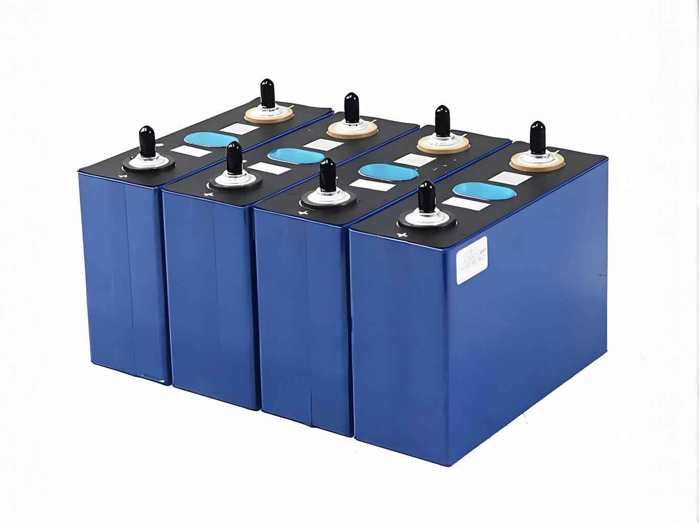
The charging profile of a typical lithium-based energy storage cell, such as the one shown, is non-linear. It consists of pre-charge, constant-current (fast charge), and constant-voltage stages. Notably, the point of maximum output power from the converter often does not coincide with the point of maximum required output voltage. During the constant-current stage, the battery voltage is moderate but the current is high, leading to high power. During the constant-voltage stage, the voltage is at its maximum but the current tapers, resulting in lower power. Therefore, selecting the worst-case design point based solely on maximum gain (voltage) is insufficient. To guarantee ZVS across the entire operational envelope of the energy storage cell, the design must be based on the maximum output power point, as this corresponds to the highest load (lowest Q), which pushes the operating point closest to the ZVS boundary.
Resonant Parameter Design Methodology
The core of the time-domain design is to select the resonant parameters (L_eq, C_eq, L_m, n) such that at the maximum output power condition, the converter operates precisely at the boundary of the ZVS region (or safely within it). This ensures that for all lighter loads (higher Q), the operation remains in the inductive Region 2.
Step 1: Defining Constraints from the Energy Storage Cell
The design specifications are derived from the connected energy storage cell’s requirements:
– Minimum input voltage: V_in_min
– Output voltage range: V_out_min to V_out_max
– Maximum output power: P_out_max
– Transformer turns ratio: n (an initial choice, often based on voltage conversion ratio)
Step 2: Relating Q at Maximum Power to Design Parameters
At the maximum power point, the equivalent AC resistance is R_eq = (8/π²) * (n² V_out_des² / P_out_max), where V_out_des is the output voltage at max power. The quality factor at this condition is:
$$Q_{CAMP} = \frac{Z_0}{R_{eq}} = \frac{\pi^2}{8} \cdot \frac{P_{out\_max}}{(M V_{in\_min})^2} \cdot Z_0$$
where M is the required gain at this point (M = n V_out_des / V_in_min).
Step 3: Enforcing the ZVS Boundary Condition at Maximum Power
To ensure ZVS at max power, the operating point (M, Q_{CAMP}) must lie on or below the pure resistive boundary Q_r. The most efficient design that maximizes Z_0 (reducing conduction losses) is achieved when Q_{CAMP} is tangent to Q_r at the intended operating gain. This condition yields the following relationships for the “hardest” operating point (M_har, Z_0_har):
$$M_{har} = \sqrt{1 + \frac{2}{\sqrt{2(k+4)}}}$$
$$Z_{0\_har} = \sqrt{ \frac{4(k + 2\sqrt{2k+4} + 4) \sqrt{2k+4} \cdot V_{in\_min}^2}{(\sqrt{2k+4} + k + 2) \pi^2 P_{out\_max} k} }$$
These equations show that once the inductance ratio k is chosen, the characteristic impedance Z_0 and the corresponding worst-case gain M_har are determined. The design rule is to ensure the actual designed Z_0 is less than or equal to Z_0_har for a chosen k.
Step 4: Time-Domain Analysis for Parameter Selection
The time-domain waveforms provide additional constraints. From the resonant current waveform at the moment t2 when i_Lr = i_Lm (secondary-side ZCS instant), the peak resonant current I1 can be expressed in terms of input/output currents and voltages. Simultaneously, the linear slope of the magnetizing current during the clamped period gives another expression for I1. Equating these provides a design equation for L_m:
$$L_m = \frac{n^2 k V_{out\_har}}{f_r [ 4k (n I_{in\_har} – I_{out\_har}) + 2\pi^2 M_{har} I_{out\_har} ]}$$
where I_in_har and I_out_har are currents at the hardest point.
Step 5: Practical Constraints and k Selection
The magnetizing inductance is also constrained by the need to fully charge/discharge the MOSFET output capacitances (C_oss) during the dead time (t_dead) to achieve ZVS:
$$L_m \leq \frac{t_{dead}}{8 f_r C_{oss\_max}}$$
Furthermore, the required maximum gain (M_max = n V_out_max / V_in_min) at the minimum switching frequency (f_n_min) imposes a final constraint on k via the gain equation (1). One selects a resonant frequency f_r and a minimum switching frequency f_s_min, then solves for the range of k that satisfies:
$$M_{max} = \frac{1}{\sqrt{ \left( 1 + \frac{2}{k} – \frac{2}{k f_{n\_min}^2} \right)^2 + \left( \frac{Z_0}{R_{eq\_min}} \right)^2 \left( 2f_{n\_min} – \frac{2}{f_{n\_min}} \right)^2 }} \geq \frac{n V_{out\_max}}{V_{in\_min}}$$
where R_eq_min corresponds to the lightest load (often at max voltage, min current).
The final design procedure is iterative: choose a tentative k; calculate Z_0_har and L_m from the equations; check constraints for dead time and max gain; adjust k and reiterate. The following table summarizes the key design equations and their purpose.
| Parameter / Equation | Purpose / Constraint |
|---|---|
| Gain: $$M = \frac{1}{\sqrt{ (1 + \frac{2}{k} – \frac{2}{k f_n^2})^2 + Q^2 (2f_n – \frac{2}{f_n})^2 }}$$ | Defines the voltage conversion ratio. Must meet specs across f_n, Q range. |
| ZVS Boundary Q: $$Q_r = \frac{\sqrt{2(1-f_n^2)(f_n^2 k + 2f_n^2 – 2)}}{2k f_n (1-f_n^2)}$$ | Defines the limit for inductive input impedance. Operation must be below this curve. |
| Worst-Case Point: $$M_{har} = \sqrt{1 + \frac{2}{\sqrt{2(k+4)}}}, Z_{0\_har}= \sqrt{ \frac{4(k + 2\sqrt{2k+4} + 4) \sqrt{2k+4} \cdot V_{in\_min}^2}{(\sqrt{2k+4} + k + 2) \pi^2 P_{out\_max} k} }$$ | Ensures ZVS at maximum power point. Guides selection of Z_0 and k. |
| Magnetizing Inductance: $$L_m = \frac{n^2 k V_{out\_har}}{f_r [ 4k (n I_{in\_har} – I_{out\_har}) + 2\pi^2 M_{har} I_{out\_har} ]}$$ | Derived from time-domain ZCS condition. Sets L_m value. |
| Dead-Time Constraint: $$L_m \leq \frac{t_{dead}}{8 f_r C_{oss\_max}}$$ | Practical limit to ensure complete charge transfer for ZVS. |
| Characteristic Impedance: $$Z_0 = \sqrt{\frac{L_{eq}}{C_{eq}}} = 2\pi f_r L_{eq} = \frac{1}{2\pi f_r C_{eq}}$$ | Fundamental design parameter linking L_eq, C_eq, and f_r. |
Simulation and Experimental Verification
A 1 kW prototype converter was designed and built to validate the methodology. The specifications, tailored for interfacing with a representative energy storage cell bank, were: Input Voltage (V_in) = 200-300 V; Output Voltage (V_out) = 20-36 V; Maximum Power (P_out_max) = 1000 W. Following the design procedure, the key parameters were determined as: Resonant Inductance L_r1 = L_r2′ = 16.4 μH; Resonant Capacitance C_r1 = C_r2′ = 0.069 μF; Magnetizing Inductance L_m = 81.8 μH; Transformer Turns Ratio n = 10:1; Resonant Frequency f_r ≈ 130 kHz; Switching Frequency Range f_s = 108 – 244 kHz.
Waveform Analysis: The experimental and simulation waveforms at the identified “hardest” points confirm the soft-switching performance. Under forward operation at V_in=200V, R_load=3Ω (≈400W), the primary switch voltage falls to zero before the gate signal rises, confirming ZVS. The secondary-side diode current naturally reaches zero before the primary resonant current equals the magnetizing current, confirming ZCS. Similar results are observed in reverse operation at the corresponding hardest point (V_in=36V, light load), demonstrating the symmetry and effectiveness of the design for bidirectional flow with an energy storage cell.
Efficiency Performance: The measured efficiency curves for both forward and reverse operation across the switching frequency range show high performance. Peak efficiency exceeds 95.5% in forward mode and 94.5% in reverse mode. The slightly lower efficiency in reverse mode is attributed to higher RMS currents. The high efficiency across the wide load and voltage range demonstrates the success of the time-domain parameter design in minimizing reactive power and switching losses, which is essential for maximizing the round-trip efficiency of an energy storage system.
Conclusion
This article has detailed a systematic time-domain design methodology for the resonant parameters of a bidirectional CLLLC converter. By approximating the topology to a symmetric Type-4 structure, the analysis complexity is reduced. Crucially, the design is anchored at the maximum output power condition rather than the maximum gain condition, which guarantees that soft-switching (ZVS and ZCS) is maintained across the entire operational range—a critical requirement for converters interfacing with energy storage cells that exhibit wide variations in voltage and current during charge and discharge cycles. The time-domain analysis, incorporating the resonant current waveform, provides precise constraints for parameter selection, ensuring optimal trade-offs between gain range, soft-switching capability, and efficiency. The design methodology is validated through the successful implementation of a 1 kW prototype, confirming its practicality and effectiveness for high-performance, bidirectional power conversion in energy storage applications.