
In recent years, perovskite solar cells have emerged as a promising third-generation photovoltaic technology due to their high power conversion efficiency, low-cost fabrication, and excellent optoelectronic properties. As a researcher in this field, I have focused on optimizing the performance of all-perovskite tandem solar cells through numerical simulations. These devices combine multiple perovskite layers with complementary bandgaps to enhance light absorption and overall efficiency. In this study, I utilized Technology Computer-Aided Design (TCAD) tools to model and simulate the behavior of single-junction and tandem perovskite solar cells. The primary goal was to identify optimal material compositions and layer thicknesses to maximize performance, with a particular emphasis on narrow-bandgap perovskite materials for the bottom sub-cell in tandem configurations. By employing drift-diffusion equations, carrier continuity equations, and Poisson’s equation, I analyzed key parameters such as open-circuit voltage, short-circuit current density, fill factor, and power conversion efficiency. This approach allowed me to explore the interplay between optical and electrical properties in these complex devices.
The simulation framework was based on the Silvaco ATLAS TCAD platform, which integrates physical models for semiconductor devices. I started by constructing a model for single-junction perovskite solar cells with an inverted (p-i-n) structure, as this configuration offers advantages like reduced hysteresis and compatibility with low-temperature processing. The basic device structure included layers such as Ag/SnO2/perovskite/NiO/ITO, where the perovskite absorber layer was varied in composition to study its impact. For the tandem cells, I designed a two-terminal monolithic structure with interconnected sub-cells, ensuring efficient carrier transport and minimal parasitic absorption. The optical model incorporated the transfer matrix method to calculate light absorption and electric field distributions, while electrical simulations accounted for recombination mechanisms like Shockley-Read-Hall and Auger processes.
To quantify the performance, I used fundamental equations that describe carrier transport and generation in semiconductors. The drift-diffusion equations for electrons and holes are given by:
$$J_n = q \mu_n n \frac{d\phi}{dx} + q D_n \frac{dn}{dx}$$
$$J_p = q \mu_p p \frac{d\phi}{dx} – q D_p \frac{dp}{dx}$$
where \( J_n \) and \( J_p \) are the electron and hole current densities, \( q \) is the elementary charge, \( \mu_n \) and \( \mu_p \) are the mobilities, \( n \) and \( p \) are the carrier concentrations, \( \phi \) is the electrostatic potential, and \( D_n \) and \( D_p \) are the diffusion coefficients. The carrier continuity equations describe the rate of change of carrier densities:
$$\frac{\partial n}{\partial t} = \frac{1}{q} \frac{\partial J_n}{\partial x} + G – R$$
$$\frac{\partial p}{\partial t} = -\frac{1}{q} \frac{\partial J_p}{\partial x} + G – R$$
where \( G \) is the generation rate and \( R \) is the recombination rate. The Poisson equation relates the electric potential to the charge density:
$$\frac{d^2 \phi}{dx^2} = -\frac{q}{\epsilon} (p – n + N_D – N_A)$$
with \( \epsilon \) being the permittivity, and \( N_D \) and \( N_A \) the donor and acceptor concentrations. For optical analysis, the photon absorption rate per unit volume at a position \( x \) and wavelength \( \lambda \) is derived from the electric field distribution \( |E(x, \lambda)|^2 \):
$$G(x, \lambda) = \frac{2\pi c}{\lambda} \alpha(\lambda) |E(x, \lambda)|^2$$
where \( c \) is the speed of light, and \( \alpha(\lambda) \) is the absorption coefficient. This formulation helps in understanding the light harvesting efficiency in perovskite solar cells.
In the initial phase, I simulated single-junction perovskite solar cells with narrow-bandgap absorbers based on MASnxPb1-xI3, where \( x \) was varied from 0 to 1. The material properties for these compositions are summarized in Table 1, including bandgap, electron affinity, effective density of states, and carrier mobilities. These parameters were critical for accurately modeling the device behavior.
| Composition (x) | Bandgap (eV) | Dielectric Constant | Electron Affinity (eV) | Nc (cm-3) | Nv (cm-3) | μn (cm²/V·s) | μp (cm²/V·s) | τn (s) | τp (s) |
|---|---|---|---|---|---|---|---|---|---|
| 0 (MAPbI3) | 1.55 | 30 | 3.93 | 2.5 × 10¹⁹ | 2.5 × 10¹⁹ | 50 | 50 | 5.0 × 10⁻⁶ | 5.0 × 10⁻⁶ |
| 0.15 | 1.42 | 27 | 3.97 | 2.5 × 10¹⁸ | 1.8 × 10¹⁸ | 2 | 1.5 | 5.0 × 10⁻⁶ | 5.0 × 10⁻⁶ |
| 0.5 | 1.20 | 20 | 4.05 | 2.5 × 10¹⁹ | 2.5 × 10¹⁹ | 3 | 2.5 | 5.0 × 10⁻⁶ | 5.0 × 10⁻⁶ |
| 0.85 | 1.17 | 13 | 4.13 | 1.5 × 10¹⁸ | 1.5 × 10¹⁸ | 5 | 5 | 5.0 × 10⁻⁶ | 5.0 × 10⁻⁶ |
| 1 (MASnI3) | 1.21 | 8.2 | 4.17 | 2.5 × 10¹⁹ | 2.5 × 10¹⁹ | 20 | 5 | 5.0 × 10⁻⁶ | 5.0 × 10⁻⁶ |
The performance metrics for these single-junction perovskite solar cells are presented in Table 2. The results indicate that MASn0.85Pb0.15I3 achieved the highest power conversion efficiency of 22.89%, with a short-circuit current density of 36.76 mA/cm², open-circuit voltage of 0.793 V, and fill factor of 78.58%. This composition was selected for further optimization in tandem structures due to its optimal bandgap and carrier dynamics.
| Composition (x) | Jsc (mA/cm²) | Voc (V) | Fill Factor (%) | Efficiency (%) |
|---|---|---|---|---|
| 0 | 22.82 | 1.119 | 81.54 | 20.82 |
| 0.15 | 29.26 | 1.023 | 75.18 | 22.49 |
| 0.5 | 30.24 | 0.744 | 77.43 | 17.42 |
| 0.85 | 36.76 | 0.793 | 78.58 | 22.89 |
| 1 | 32.17 | 0.758 | 78.41 | 19.10 |
Next, I investigated the effect of layer thickness on the performance of single-junction perovskite solar cells. The absorber layer thickness was varied from 100 nm to 900 nm, while the hole transport layer (NiO) and electron transport layer (SnO2) thicknesses were optimized separately. The power conversion efficiency as a function of perovskite layer thickness showed a rapid increase up to 500 nm, followed by a gradual saturation beyond 900 nm. To balance performance and practical fabrication constraints, I fixed the absorber thickness at 550 nm for subsequent simulations. For the transport layers, a thickness scan revealed that thinner layers generally yielded better results; specifically, 10 nm for NiO and 20 nm for SnO2 were chosen to minimize resistive losses and enhance carrier extraction.
Building on these findings, I proceeded to model two-terminal all-perovskite tandem solar cells. The top sub-cell employed wide-bandgap perovskite materials from the CsPbI3-yBry family (with y = 0, 1, 2), which offer tunable bandgaps and good stability. The bottom sub-cell used the optimized MASn0.85Pb0.15I3 absorber. The tandem structure was designed as Ag/SnO2/narrow-bandgap perovskite/NiO/ITO/SnO2/wide-bandgap perovskite/NiO/ITO, where the ITO layer served as a tunnel junction for interconnecting the sub-cells. The performance of these tandem perovskite solar cells was evaluated based on current matching between the top and bottom sub-cells, as this is crucial for maximizing efficiency in series-connected devices.
Table 3 compares the performance parameters for different top-cell materials. CsPbI3 (y = 0) demonstrated the highest efficiency of 32.58%, with a short-circuit current density of 16.41 mA/cm², open-circuit voltage of 2.17 V, and fill factor of 87.9%. This combination achieved current matching, where both sub-cells contributed equally to the total current output.
| Top-Cell Material | Jsc (mA/cm²) | Voc (V) | Fill Factor (%) | Efficiency (%) |
|---|---|---|---|---|
| CsPbI3 | 16.41 | 2.17 | 87.9 | 32.58 |
| CsPbI2Br | 15.26 | 2.183 | 87.34 | 30.18 |
| CsPbIBr2 | 13.53 | 2.202 | 84.62 | 25.21 |
To further optimize the tandem perovskite solar cell, I varied the thicknesses of the top and bottom absorber layers. The power conversion efficiency was calculated as a function of these thicknesses, and the optimal values were found to be 260 nm for CsPbI3 and 550 nm for MASn0.85Pb0.15I3. At these thicknesses, the current densities of both sub-cells were matched at 16.41 mA/cm², leading to the highest efficiency. Deviations from these thicknesses resulted in current mismatch and reduced performance, highlighting the importance of precise layer control in tandem perovskite solar cell design.
The optical behavior of the tandem perovskite solar cell was analyzed by examining the photon absorption rate and the electric field distribution within the device. The absorption spectra showed that the top cell primarily absorbed photons in the 300–500 nm wavelength range, while the bottom cell absorbed longer wavelengths (500–900 nm). The electric field distribution, calculated using the transfer matrix method, revealed interference patterns due to multiple reflections at the interfaces. These patterns influenced the light absorption profile and were optimized by adjusting the layer thicknesses. For instance, at the optimal thicknesses, the electric field was more uniformly distributed, enhancing absorption in both sub-cells.
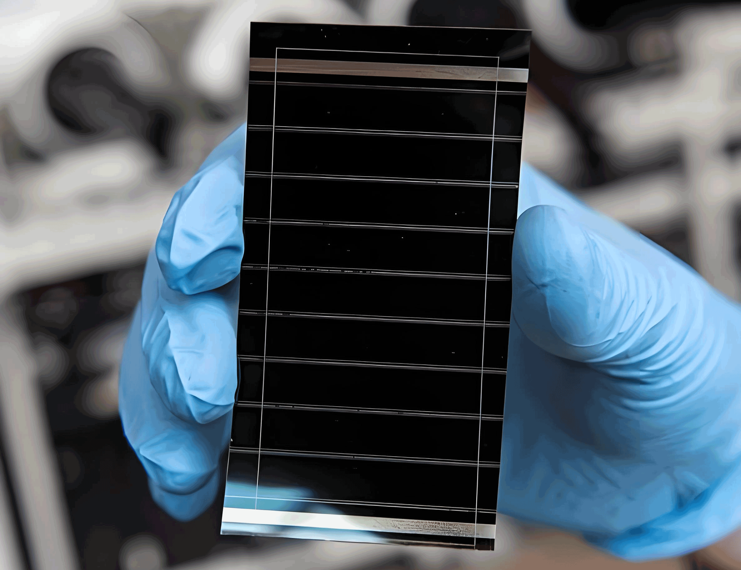
In conclusion, my simulation study demonstrates that all-perovskite tandem solar cells can achieve high efficiencies through careful optimization of material compositions and layer thicknesses. The narrow-bandgap perovskite MASn0.85Pb0.15I3 is an ideal candidate for the bottom sub-cell, and when paired with CsPbI3 as the top sub-cell, the tandem structure reaches a power conversion efficiency of 32.58%. The TCAD-based approach provided valuable insights into the optoelectronic properties, such as electric field distributions and carrier dynamics, which are essential for guiding experimental efforts. Future work could explore interface engineering, defect passivation, and scalability to further improve the performance of perovskite solar cells. This research underscores the potential of all-perovskite tandem configurations in advancing photovoltaic technology and achieving higher energy conversion efficiencies.