
In recent years, organic-inorganic hybrid perovskite materials have garnered significant attention due to their exceptional optoelectronic properties. Perovskite solar cells, fabricated from these materials, have achieved remarkable power conversion efficiencies (PCE) of up to 26.1%, closely rivaling silicon-based solar cells. The high efficiency of perovskite solar cells is attributed to their long carrier diffusion lengths, high absorption coefficients, and tunable bandgaps. The quality of the perovskite film is crucial, as it directly influences the PCE and stability of the device. In a typical perovskite solar cell, photo-induced carriers generated within the perovskite layer separate and migrate to charge transport layers, necessitating films with large grains, high morphological quality, low defect density, and high carrier mobility for optimal performance. Thus, strategies to fabricate high-performance perovskite films are a focal point of current research.
Solution-processed polycrystalline perovskite films often exhibit defects at grain boundaries after high-temperature annealing, leading to uncoordinated ions that act as recombination centers, impairing charge extraction and device performance. To address this, interface defect passivation has emerged as a vital method to reduce defect density in perovskite solar cells. Recent studies have highlighted the benefits of incorporating excess lead iodide (PbI2) into perovskite precursors to enhance device efficiency. For instance, molecular dynamics simulations suggest that excess PbI2 can improve performance, and experimental work has shown that adding surplus PbI2 to MAPbI3 precursors significantly boosts PCE from 14.14% to 16.80%. However, the impact of excess PbI2 on perovskite solar cells is complex and depends on both the amount added and the film processing conditions. In this study, we investigate the effects of varying PbI2 concentrations in the perovskite precursor solution on the performance of inverted perovskite solar cells. We demonstrate that controlled amounts of excess PbI2 can passivate defects, reduce hysteresis, and enhance key parameters such as open-circuit voltage (VOC) and fill factor (FF), leading to a champion PCE of 22.90%.
We fabricated inverted perovskite solar cells with the structure ITO/MeO-2PACz/PVSK/PC61BM/BCP/Ag. The ITO substrates were cleaned sequentially with detergent, deionized water, acetone, and ethanol via ultrasonication for 20 minutes each, followed by drying with nitrogen and UV ozone treatment for 30 minutes. The hole transport layer was formed by spin-coating a solution of MeO-2PACz (0.5 mg/mL in ethanol) at 3,000 rpm for 30 seconds, followed by annealing at 100°C for 10 minutes. The perovskite precursor solutions were prepared with different PbI2 concentrations: a control group with a baseline amount (572 mg), and experimental groups with additional 0.05 mM and 0.10 mM of PbI2 (594.7 mg and 617.74 mg, respectively). The base composition included MABr, MACl, CsI, FAI, PbBr2, and PbI2 dissolved in a mixture of DMF and DMSO (4:1 volume ratio), stirred at 60°C for 1 hour. The perovskite films were deposited in a nitrogen-filled glovebox using a one-step anti-solvent method, with a two-step spin-coating program: 1,000 rpm for 5 seconds and 4,000 rpm for 30 seconds. Chlorobenzene (150 μL) was applied as an anti-solvent 15 seconds before the end of the process, and the films were annealed at 100°C for 40 minutes. The electron transport layer was formed by spin-coating PCBM (23 mg/mL in chlorobenzene) at 4,000 rpm for 30 seconds and annealing at 70°C for 10 minutes, followed by BCP (5 mg/mL in isopropanol) at 5,000 rpm for 30 seconds. Finally, an 80 nm thick Ag electrode was deposited via thermal evaporation under a vacuum of 1.33 × 10⁻⁵ Pa.
Characterization of the films and devices included scanning electron microscopy (SEM) for surface and cross-sectional morphology, X-ray diffraction (XRD) for structural analysis, UV-visible absorption spectroscopy for optical properties, steady-state and time-resolved photoluminescence (PL and TRPL) for carrier dynamics, space charge-limited current (SCLC) measurements for defect density quantification, and transient photocurrent (TPC) and transient photovoltage (TPV) for charge recombination and extraction studies. Photovoltaic performance was evaluated using a solar simulator under AM 1.5 illumination, with J-V curves recorded using a Keithley 2400 source meter. A mask with an area of 0.06 cm2 defined the active area, and scans were performed from -0.05 V to 1.2 V (forward) and 1.2 V to -0.05 V (reverse) at a rate of 10 mV/s to assess hysteresis.
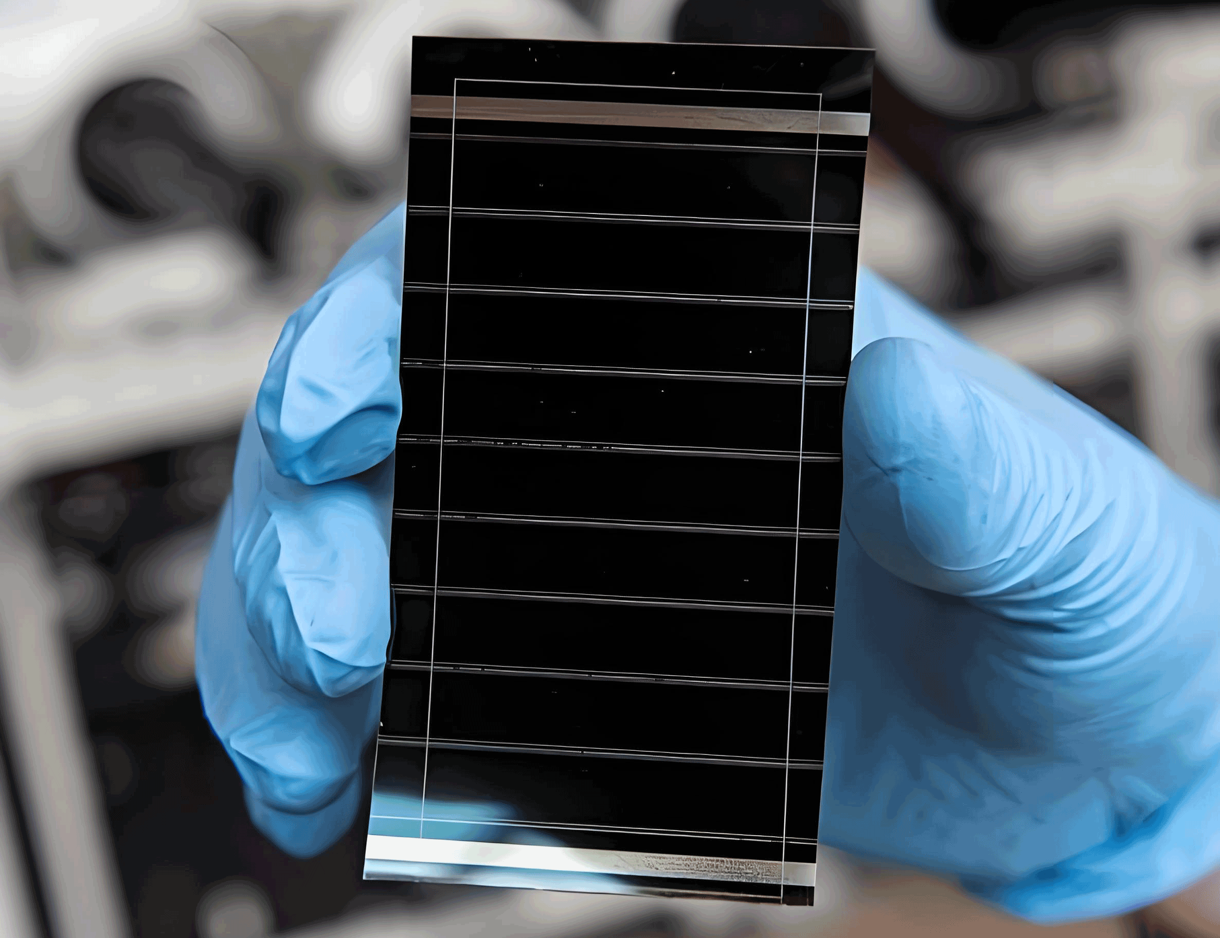
The morphology of the perovskite films was critically examined using SEM. The control film exhibited relatively smaller grains and some surface irregularities, whereas the films with excess PbI2 showed larger, more uniform grains and improved coverage. This suggests that the additional PbI2 promotes better crystallization and reduces grain boundary defects. In particular, the experimental group with 0.05 mM excess PbI2 displayed the most homogeneous morphology, with minimal pinholes. The cross-sectional images confirmed a compact and continuous perovskite layer, essential for efficient charge transport in perovskite solar cells. To further illustrate the morphological improvements, we include a representative image below:
XRD analysis revealed that all films exhibited characteristic peaks of α-FAPbI3 at 2θ = 14.08°, 28.40°, and 31.86°, corresponding to the (110), (220), and (310) planes, respectively. The introduction of excess PbI2 did not shift these peaks, indicating that the perovskite crystal structure remained intact. However, the intensity of these peaks increased with higher PbI2 concentrations, suggesting enhanced crystallinity and reduced disorder. No additional peaks corresponding to PbI2 phases were prominently observed, which may be due to the homogeneous distribution of excess PbI2 at grain boundaries rather than as separate crystalline domains. This aligns with the passivation mechanism where PbI2 segregates to interfaces, mitigating defects in perovskite solar cells.
UV-visible absorption spectroscopy showed that all films had similar optical bandgaps, approximately 1.55 eV, consistent with the typical bandgap of FAPbI3-based perovskites. However, the films with excess PbI2 demonstrated slightly stronger absorption in the visible range, attributable to the larger grain sizes and denser morphology, which reduce light scattering and improve photon harvesting. This enhancement in absorption can contribute to higher photocurrents in perovskite solar cells, although the primary benefits were observed in voltage and fill factor improvements.
Steady-state PL measurements indicated a significant increase in PL intensity for films with excess PbI2 compared to the control. Specifically, the PL intensity for the 0.05 mM excess PbI2 film was approximately four times higher than that of the control, indicating reduced non-radiative recombination. TRPL decay curves were fitted using a bi-exponential model:
$$ I(t) = I_0 + A_1 \exp\left(-\frac{t – t_1}{\tau_1}\right) + A_2 \exp\left(-\frac{t – t_1}{\tau_2}\right) $$
where A1 and A2 are amplitudes, and τ1 and τ2 represent the fast and slow decay lifetimes, respectively. The average carrier lifetime (τave) was calculated as:
$$ \tau_{\text{ave}} = \frac{A_1 \tau_1^2 + A_2 \tau_2^2}{A_1 \tau_1 + A_2 \tau_2} $$
The control film had a τave of 1.11 μs, while the film with 0.05 mM excess PbI2 exhibited a longer τave of 1.96 μs. This increase in carrier lifetime confirms that excess PbI2 effectively passivates defects, suppressing carrier recombination in the perovskite solar cell films. The slow decay component (τ2), associated with bulk defects, showed a notable extension, underscoring the role of PbI2 in improving bulk quality.
To delve deeper into the charge recombination dynamics, we performed TPV and TPC measurements. TPV decay curves were fitted with a bi-exponential function, revealing that the dominant recombination time constant increased from 3.28 ms for the control device to 6.20 ms for the device with 0.05 mM excess PbI2. This prolonged decay time indicates suppressed interface recombination, facilitated by PbI2 passivation at the perovskite/PC61BM interface. TPC measurements showed that the charge extraction time decreased from 26.77 μs for the control to 11.23 μs for the optimized device, demonstrating enhanced charge collection efficiency. These results collectively highlight that excess PbI2 reduces trap-assisted recombination and improves charge transport in perovskite solar cells.
SCLC measurements on hole-only devices (ITO/PEDOT:PSS/PVSK/Spiro-OMeTAD/Au) were used to quantify the defect density (Ntrap) in the perovskite films. The J-V curves in the dark exhibited a trap-fill limit voltage (VTFL), from which Ntrap was derived using the formula:
$$ N_{\text{trap}} = \frac{2V_{\text{TFL}} \epsilon_r \epsilon_0}{e L^2} $$
where ε0 is the vacuum permittivity, εr is the relative permittivity of perovskite (assumed as 32), e is the elementary charge, and L is the film thickness (500 nm). The VTFL decreased from 0.20 V for the control to 0.07 V for the 0.05 mM excess PbI2 film, corresponding to a reduction in Ntrap from 5.5 × 1015 cm−3 to 1.92 × 1015 cm−3. This substantial decrease in defect density validates the passivation effect of PbI2 in perovskite solar cells.
The open-circuit voltage (VOC) dependence on light intensity was analyzed to understand recombination mechanisms. The relationship is given by:
$$ V_{\text{OC}} = V_{\text{S}} + \frac{n k_B T}{q} \ln \left( \frac{P_\lambda}{P_S} \right) $$
where VS is the VOC at standard illumination, n is the diode ideality factor, kBT/q is the thermal voltage, Pλ is the light intensity, and PS is the standard irradiance. The slope of the VOC vs. ln(Pλ) plot decreased from 1.89 kBT/q for the control to 1.35 kBT/q for the device with 0.05 mM excess PbI2, indicating a lower ideality factor and reduced non-radiative recombination. This further supports the role of PbI2 in minimizing voltage losses in perovskite solar cells.
The photovoltaic performance of the devices was systematically evaluated. The table below summarizes the key parameters for the control and experimental groups under reverse scan conditions:
| Sample | JSC (mA/cm2) | VOC (V) | FF (%) | PCE (%) | Hysteresis Index (HI) |
|---|---|---|---|---|---|
| Control | 24.50 | 1.08 | 77.60 | 20.45 | 7.40 |
| 0.05 mM Excess PbI2 | 24.20 | 1.15 | 80.06 | 22.90 | 3.35 |
| 0.10 mM Excess PbI2 | 23.80 | 1.14 | 79.50 | 21.80 | 4.20 |
As shown, the control device had a PCE of 20.45%, with a JSC of 24.50 mA/cm2, VOC of 1.08 V, and FF of 77.60%. With 0.05 mM excess PbI2, the PCE increased to 22.90%, driven by a higher VOC of 1.15 V and FF of 80.06%, while JSC slightly decreased to 24.20 mA/cm2. This JSC reduction is likely due to the wider bandgap of PbI2 at the interface, which may impede electron transport slightly. However, the overall improvement in VOC and FF outweighs this effect, resulting in a net gain in efficiency. Further increasing PbI2 to 0.10 mM led to a slight decline in PCE to 21.80%, indicating an optimal concentration beyond which performance may degrade due to excessive PbI2 accumulation. The hysteresis index (HI), calculated as:
$$ \text{HI} = \frac{\text{PCE}_{\text{reverse}} – \text{PCE}_{\text{forward}}}{\text{PCE}_{\text{reverse}}} $$
decreased from 7.40% for the control to 3.35% for the 0.05 mM excess PbI2 device, demonstrating suppressed hysteresis. This reduction is attributed to faster charge extraction and diminished ion migration at the interfaces, facilitated by PbI2 passivation.
The enhanced performance in perovskite solar cells with excess PbI2 can be explained by the passivation of defects at grain boundaries and interfaces. PbI2 forms a type-I band alignment with the perovskite, which blocks hole injection into the electron transport layer and reduces interface recombination. This passivation effect lowers the defect density, as evidenced by SCLC and TRPL results, leading to higher VOC and FF. Additionally, the improved morphology and crystallinity contribute to better charge transport and reduced hysteresis. It is important to note that the amount of excess PbI2 must be carefully optimized, as excessive amounts can lead to charge transport barriers and JSC losses. Our findings underscore the delicate balance required in modulating PbI2 content for high-performance perovskite solar cells.
In conclusion, we have demonstrated that incorporating excess PbI2 into the perovskite precursor solution is an effective strategy to enhance the performance of inverted perovskite solar cells. Through comprehensive characterization, we found that optimal amounts of PbI2 (0.05 mM excess) passivate defects, reduce non-radiative recombination, and improve charge extraction, resulting in a champion PCE of 22.90% with minimal hysteresis. The reduction in defect density and suppression of interface recombination are key factors driving these improvements. This work provides valuable insights into the role of PbI2 in defect passivation and highlights a simple, reliable approach to advancing perovskite solar cell technology. Future studies could explore combinations with other passivation agents to further push the efficiency and stability boundaries of perovskite solar cells.