
The global push towards sustainable energy has propelled photovoltaic (PV) technology to the forefront of the power generation landscape. The efficiency and longevity of a photovoltaic solar system are fundamentally dependent on the quality of its individual components, starting with the silicon wafer. Surface defects in these wafers, such as micro-cracks, chips, or impurities, can severely degrade the performance and reliability of the final PV module. Therefore, accurate and rapid defect detection is a critical bottleneck in the manufacturing process. This article, from my perspective in applied industrial AI, details the research and practical application of a visual machine learning system designed to automate and enhance the inspection of solar photovoltaic wafers, a cornerstone of any modern solar system. This approach leverages big data and deep learning to replace traditional manual inspection, offering unprecedented speed, consistency, and accuracy for building more robust photovoltaic solar system infrastructure.
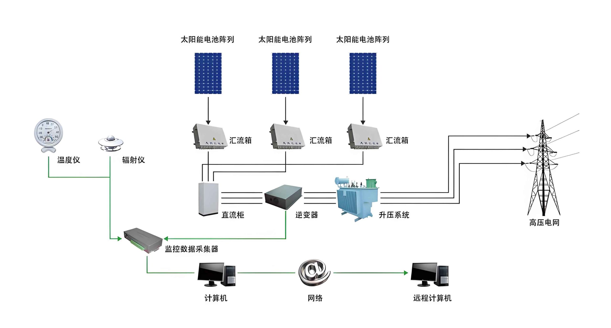
Defect Typology in Photovoltaic Wafers
Understanding the types of defects is crucial for building an effective detection model. Common defects identified during Electroluminescence (EL) testing, which will be discussed later, can be categorized as follows:
| Defect Category | Specific Types | Visual Signature (EL Image) | Potential Impact on Solar System Performance |
|---|---|---|---|
| Cracks & Fractures | Linear Cracks (Hidden/Visible), Chipped Corners | Dark, linear or angular interruptions in the uniform bright cell pattern. | Creates high resistance paths, reduces active area, can lead to catastrophic failure under thermal stress. |
| Material Impurities & Inhomogeneities | Black Spots, Dark Areas, Dark Lines | Localized dark regions of varying size and shape against the bright background. | Act as recombination centers for charge carriers, reducing current output and overall cell efficiency. |
| Process-Induced Defects | Sintering Faults, Finger Interruptions, Edge Isolation Issues | Irregular patterns, discontinuous grid lines, or non-uniform brightness at edges. | Increases series resistance, lowers fill factor, and can cause localized heating (hot spots) in the solar system module. |
| Micro-Damage | Scratches, Pits | Fine, dark, often irregular lines or small dots. | May not immediately fail but can propagate into larger cracks, undermining the long-term reliability of the solar system installation. |
The Foundation: Electroluminescence (EL) Imaging
The primary data source for our visual inspection system is Electroluminescence (EL) imaging. This non-destructive technique is essential for revealing subsurface defects not visible to the naked eye. The principle involves forward-biasing the finished solar cell by applying a small external voltage, typically inducing a current of 1-40 mA. This injected current causes electrons and holes to recombine radiatively within the semiconductor, emitting photons primarily in the near-infrared spectrum. A sensitive CCD or InGaAs camera captures this emitted light, producing a high-contrast image where bright areas correspond to regions of efficient charge carrier recombination and high material quality, while dark areas indicate defects that act as non-radiative recombination centers.
The quality of the EL image is paramount for the subsequent machine learning analysis. The signal-to-noise ratio is critical, as the photon flux is relatively low. The process can be conceptually modeled. The luminescence intensity \(I_{EL}(x,y)\) at a pixel location \((x,y)\) is proportional to the local external quantum efficiency and the injected current density \(J\):
$$I_{EL}(x,y) \propto \text{EQE}(x,y) \cdot J(x,y)$$
Defects locally reduce the external quantum efficiency \(\text{EQE}\), leading to a drop in \(I_{EL}\) and appearing as dark features. This rich, information-dense image data forms the perfect input for a convolutional neural network (CNN), enabling the automated and quantitative assessment of wafer health critical for a reliable solar system.
Architecture of the Visual Machine Learning System
The core of our solution is a scalable, visual machine learning platform designed for industrial deployment. The system architecture must support the entire pipeline from data ingestion and model training to real-time inference and continuous improvement. The following table summarizes the key components and their functions.
| System Layer | Key Components | Function |
|---|---|---|
| Data Acquisition & Storage | EL Test Stations, IoT Gateways, Distributed File System (e.g., HDFS), Data Lake | Collects high-throughput image data from production lines, performs initial preprocessing (scaling, timestamping), and stores images and metadata in a scalable repository for historical analysis. |
| Data Preparation & Labeling | Interactive Labeling UI, Data Augmentation Engine (Rotation, Flip, Noise, Contrast Adjustment) | Provides a GUI for experts to draw bounding boxes/polygons and assign defect class labels. Augments the training dataset synthetically to improve model robustness and generalization for the diverse conditions in a solar system manufacturing line. |
| Automated Model Training & Tuning | Neural Architecture Search (NAS) framework (e.g., NNI), Hyperparameter Optimizer, Distributed Training Cluster (GPUs) | Automates the search for optimal CNN architectures and hyperparameters (learning rate, batch size, optimizer settings). Manages parallel trials to efficiently find the best model, significantly reducing the data scientist’s manual effort. |
| Model Registry & Deployment | Model Versioning Database, Containerization (Docker), Microservices API | Stores, versions, and manages trained models. Packages models into containers for consistent deployment as inference microservices on production servers or edge devices. |
| Real-time Inference Service | High-performance Inference Engine (e.g., TensorRT, ONNX Runtime), Load Balancer | Receives preprocessed EL images from the production line via API calls, executes the trained CNN model with low latency (milliseconds), and returns defect classification, localization, and quantitative metrics (e.g., defect area, length). |
| Feedback & Monitoring Loop | Prediction Logging, Drift Detection, Active Learning Interface | Logs all predictions and confidence scores. Monitors for model performance drift over time. Flags uncertain predictions for expert review, feeding new labeled data back into the training pipeline to continuously improve the solar system quality control model. |
Core Algorithm: Convolutional Neural Networks (CNN) for Defect Detection
We employ Convolutional Neural Networks (CNNs), the state-of-the-art for image analysis, as the core algorithmic engine. A CNN automatically learns hierarchical features from raw pixel data, from simple edges and textures in early layers to complex defect patterns in deeper layers. The process for a single convolutional layer can be described as follows. An input feature map (or image) \(I\) is convolved with a learnable kernel (filter) \(K\) to produce an output feature map \(O\).
$$O(x,y) = (I * K)(x,y) = \sum_{i} \sum_{j} I(x+i, y+j) \cdot K(i, j)$$
This operation is followed by a non-linear activation function, such as the Rectified Linear Unit (ReLU):
$$\text{ReLU}(z) = \max(0, z)$$
Pooling layers (e.g., Max Pooling) are then used for spatial down-sampling, reducing computational load and providing translation invariance. For defect detection and segmentation, we utilize a specific CNN architecture called U-Net or similar encoder-decoder networks. These networks first compress the image into a high-level representation (encoder) and then progressively upsample it (decoder) to produce a pixel-wise classification map. The final layer uses a softmax activation for multi-class segmentation or a sigmoid for binary defect/no-defect maps.
The loss function for training such a network, particularly for pixel-wise defect segmentation, is often a combination like the Dice Loss or a weighted cross-entropy to handle class imbalance (where defect pixels are far fewer than background pixels). For a binary case, the Dice Coefficient \(D\) measures the overlap between the predicted segmentation \(P\) and the ground truth \(G\):
$$D = \frac{2 |P \cap G|}{|P| + |G|}$$
And Dice Loss \(L_{Dice}\) is defined as:
$$L_{Dice} = 1 – D$$
Minimizing this loss during training forces the model to produce predictions that spatially align perfectly with the annotated defects, which is essential for precise quality assessment in the solar system supply chain.
Application Workflow in Solar System Wafer Production
The integration of the visual machine learning system into the PV wafer production line follows a meticulous, multi-stage workflow designed for closed-loop continuous improvement. This end-to-end process ensures that the intelligence of the system evolves alongside manufacturing practices.
| Stage | Input | Process & Action | Output |
|---|---|---|---|
| 1. Historical Data Aggregation | Archived EL images (50,000+), historical inspection logs. | Gather and upload years of production data containing confirmed defect samples. Categorize data by suspected defect type. | A centralized, labeled (or pre-label-able) historical image database for the solar system component factory. |
| 2. Interactive Data Labeling | Raw historical EL images. | Quality engineers use the system’s GUI to draw precise contours around defects (e.g., cracks, black spots) and assign class labels. This creates the “ground truth” dataset. | A high-quality, expertly annotated dataset for supervised learning. This is the most critical step for model accuracy. |
| 3. Automated Model Training & Validation | Annotated dataset (split into training/validation sets). | The system performs automated feature engineering, neural architecture search, and hyperparameter tuning. Multiple CNN models are trained and evaluated on the validation set using metrics like precision, recall, and mIoU (mean Intersection over Union). | A validated, production-ready CNN model file with documented performance metrics exceeding predefined thresholds (e.g., >95% accuracy for major defect classes). |
| 4. Offline Testing & Calibration | New, unseen batches of EL images from recent production. | The trained model is deployed in a staging environment. Its predictions are compared against expert inspections for a new set of wafers. Discrepancies are analyzed, and model calibration or additional targeted training is performed if necessary. | A fully calibrated and benchmarked model, proven to handle the variance and novel edge cases found in live production for the solar system. |
| 5. Real-Time Production Deployment | Live stream of EL images from the production line test station. | The model is containerized and hosted as a microservice. Each new wafer image is preprocessed (cropped, normalized) and sent to the service for inference in milliseconds. Defect classification, location, and quantitative metrics are returned. | Real-time Pass/Fail decisions, detailed defect reports, and binning of wafers. Data is fed into MES (Manufacturing Execution System). |
| 6. Continuous Monitoring & Active Learning | Stream of model predictions and confidence scores. | The system monitors prediction confidence. Low-confidence samples or samples where the model’s prediction contradicts a subsequent process outcome are flagged. These are periodically reviewed by experts and fed back into the labeling pipeline. | A continuously improving model that adapts to new materials, process changes, or previously rare defect types, perpetually enhancing the quality control of the solar system manufacturing process. |
Conclusion and Measured Impact
The implementation of this visual machine learning system for photovoltaic wafer defect detection represents a significant leap forward in smart manufacturing for the renewable energy sector. By transforming the subjective, slow, and fatiguing task of manual visual inspection into an automated, data-driven, and precise analytical process, we have achieved concrete and substantial benefits that directly enhance the value proposition of a photovoltaic solar system.
The results from production deployment are compelling: a reduction of over 50% in manual inspection labor requirements, a 100% increase in the capability to inspect every single wafer (full inspection), and a 200% improvement in inspection throughput. Most importantly, the automatic recognition accuracy for critical defects in multi-crystalline silicon wafers now consistently exceeds 95%. This system not only screens out defective components with high reliability but also generates a rich stream of quantitative defect data. This data provides invaluable feedback for process engineers to pinpoint root causes in the production chain, enabling continuous optimization of the manufacturing parameters. This closed-loop intelligence is key to driving down costs and improving the performance and durability of every photovoltaic solar system deployed.
The success of this application underscores the transformative potential of visual machine learning in industrial quality control. It serves as a foundational model that can be extended to other stages of PV module production and to adjacent industries requiring high-precision visual inspection. As the technology matures and integrates further with other Industry 4.0 systems, the vision of fully automated, “lights-out” manufacturing for critical components like those in a photovoltaic solar system moves from aspiration to an achievable standard, ensuring a more sustainable and efficient energy future.