
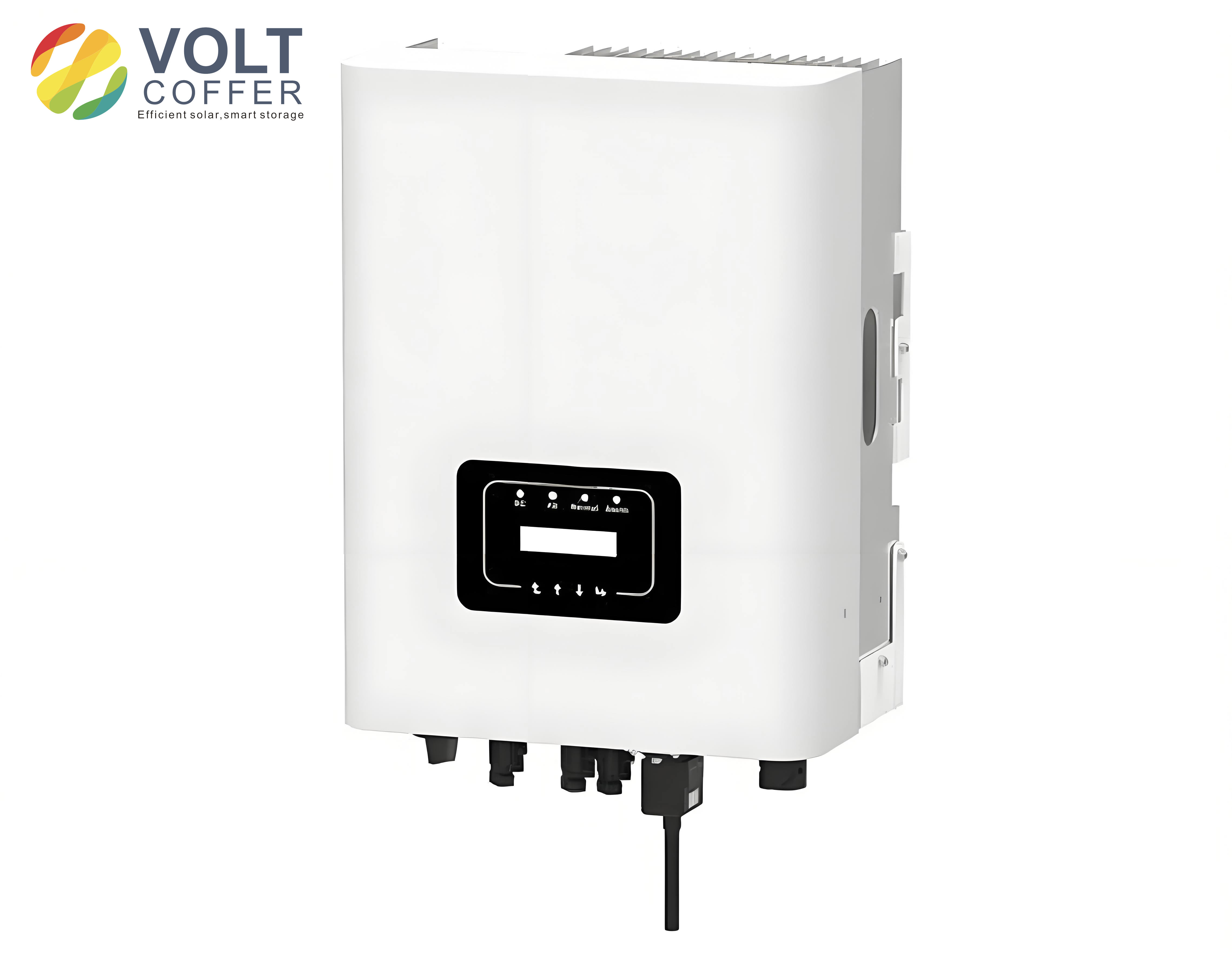
The integration of distributed renewable energy sources, primarily through power electronic converters known as grid connected inverters, is a cornerstone of the modern power grid. These devices are responsible for converting DC power from sources like photovoltaic arrays into high-quality AC power synchronized with the utility grid. The performance and stability of a grid connected inverter are paramount, directly influencing grid power quality and the safe operation of distributed generation systems. Among various topologies, the LCL-filter-based three-phase grid connected inverter is widely adopted due to its superior high-frequency harmonic attenuation with smaller, cost-effective passive components compared to a simple L-filter design.
However, the transition from analog to digital control systems, while bringing unparalleled flexibility and intelligence, introduces inherent challenges. The computation and modulation delays inherent in digital control loops can significantly degrade system performance. These delays alter the phase characteristics of the control loop, potentially destabilizing the system, especially when active damping or high-bandwidth current control is employed. They also limit the achievable control bandwidth, leading to increased harmonic distortion in the output current of the grid connected inverter. Therefore, minimizing digital delay is a critical research objective for enhancing the robustness and power quality of modern grid connected inverter systems.
This article presents the design and implementation of an experimental platform centered on achieving ultra-low digital delay in a three-phase LCL-type grid connected inverter. The core innovation lies in leveraging the parallel processing architecture and hardware-configurable nature of a Field-Programmable Gate Array (FPGA) to implement a real-time sampling and modulation strategy, drastically reducing the computation delay compared to conventional methods implemented on sequential processors like Digital Signal Processors (DSPs).
System Architecture and Hardware Design
The experimental platform is architected as a heterogeneous processing system, strategically dividing tasks between a DSP and an FPGA to optimize performance. The overall system block diagram is illustrated below, showcasing the synergy between control algorithms and high-speed signal generation.
1.1 Heterogeneous Control Architecture
The platform utilizes a Texas Instruments DSP TMS320F28377D as the primary algorithm computation unit and a Pango Micro PGL25G series FPGA as the high-speed peripheral and pulse-width modulation (PWM) generation unit. This division of labor is crucial:
- DSP (Master Controller): Executes high-level control algorithms. Its primary tasks include:
- System sequencing (start-up/shutdown procedures).
- Real-time sampling of grid voltages ($$v_{ga}, v_{gb}, v_{gc}$$), grid currents ($$i_{ga}, i_{gb}, i_{gc}$$), and DC-link voltage ($$V_{dc}$$).
- Execution of a Phase-Locked Loop (PLL) for grid synchronization.
- Implementation of current control loops in the synchronous reference frame (d-q).
- Calculation of three-phase voltage reference signals ($$v_{a}^{ref}, v_{b}^{ref}, v_{c}^{ref}$$) and communication of these to the FPGA.
- FPGA (Slave Co-processor & I/O Manager): Handles time-critical, parallelizable tasks. Its core functions are:
- Receiving voltage reference commands from the DSP via a high-speed parallel or serial communication interface.
- Implementing the ultra-low-delay Space Vector Pulse Width Modulation (SVPWM) algorithm using a real-time sampling method.
- Generating and outputting the final, precisely timed PWM signals to the gate driver circuits.
- Managing local digital I/O, handling fault protection signals (e.g., overcurrent, DC-link overvoltage), and interrupting the DSP in case of faults.
This architecture allows the DSP to focus on complex, floating-point arithmetic for control, while the FPGA ensures deterministic, jitter-free execution of the modulation scheme with minimal latency.
| Component Category | Part / Model | Key Function |
|---|---|---|
| Main Control Chip | TMS320F28377D (DSP) | System control, algorithm execution, data processing. |
| Logic & PWM Chip | Pango Micro PGL25G (FPGA) | Ultra-low-delay SVPWM, digital I/O management, fault protection. |
| Power Stage | Custom 3-Phase Full-Bridge | DC-AC power conversion using MOSFETs/IGBTs. |
| Gate Driver | IXYS IXDND609SI + ACPL-4800 | Isolates and amplifies FPGA PWM signals to drive power switches. |
| Current Sensor | Tamura TBCTP series (Hall-effect) | Non-invasive measurement of grid/inductor currents. |
| Signal Conditioning | THS4524 (Fully-Diff Amp) | Amplifies and buffers current sensor signals for ADC. |
| Analog-to-Digital Converter | ADS8364 (16-bit, 6-Channel) | Simultaneously samples multiple analog signals (currents, voltages). |
1.2 Power Circuit and LCL Filter
The main power circuit is a standard three-phase, two-level voltage source inverter (VSI). The DC input ($$V_{dc}$$) is switched by six power devices (S1 to S6) to produce three-phase AC voltages. The inverter is connected to the grid through an LCL filter, which provides superior attenuation of switching-frequency harmonics. The dynamics of the LCL filter are critical for controller design. The inverter-side inductor ($$L_1$$), capacitor ($$C_f$$), and grid-side inductor ($$L_g$$) create a third-order system. The following equations describe the filter behavior in the stationary $$\alpha\beta$$ frame:
Inverter-side inductor voltage:
$$ v_{inv,\alpha\beta} – v_{c,\alpha\beta} = L_1 \frac{d i_{1,\alpha\beta}}{dt} $$
Capacitor current:
$$ i_{c,\alpha\beta} = C_f \frac{d v_{c,\alpha\beta}}{dt} = i_{1,\alpha\beta} – i_{g,\alpha\beta} $$
Grid-side inductor voltage:
$$ v_{c,\alpha\beta} – v_{g,\alpha\beta} = L_g \frac{d i_{g,\alpha\beta}}{dt} $$
Where $$v_{inv}$$ is the inverter output voltage, $$v_c$$ is the capacitor voltage, $$v_g$$ is the grid voltage, $$i_1$$ is the inverter-side current, and $$i_g$$ is the grid-side current (the controlled output).
| Parameter | Symbol | Value |
|---|---|---|
| Rated Grid Voltage (Line-to-Line) | $$V_{g,LL}$$ | 380 V (RMS) |
| DC-Link Voltage | $$V_{dc}$$ | 520 V |
| Grid-Side Inductor | $$L_g$$ | 1.9 mH |
| Inverter-Side Inductor | $$L_1$$ | 1.6 mH |
| Filter Capacitor | $$C_f$$ | 5 µF |
| Switching Frequency | $$f_{sw}$$ | 10 kHz |
| Control/Sampling Frequency | $$f_s$$ | 10 kHz |
Control Strategy and Software Design
The control objective for the grid connected inverter is to regulate the active and reactive power injected into the grid by controlling the grid currents. A synchronous reference frame (dq) current control strategy is employed due to its ability to achieve zero steady-state error for sinusoidal references.
2.1 Overall Control Loop Structure
The closed-loop control structure implemented on the DSP is depicted in the block diagram and governed by the following sequence:
- Grid Synchronization: A PLL extracts the grid angle $$\theta = \omega t$$ from the measured grid voltages, enabling transformation into the synchronous rotating dq frame.
- Current Measurement & Transformation: The three-phase grid currents ($$i_{ga}, i_{gb}, i_{gc}$$) are measured, transformed to the $$\alpha\beta$$ frame (Clarke transformation), and then to the dq frame (Park transformation) using $$\theta$$.
$$ \begin{bmatrix} i_{\alpha} \\ i_{\beta} \end{bmatrix} = \frac{2}{3} \begin{bmatrix} 1 & -\frac{1}{2} & -\frac{1}{2} \\ 0 & \frac{\sqrt{3}}{2} & -\frac{\sqrt{3}}{2} \end{bmatrix} \begin{bmatrix} i_{ga} \\ i_{gb} \\ i_{gc} \end{bmatrix} $$
$$ \begin{bmatrix} i_{d} \\ i_{q} \end{bmatrix} = \begin{bmatrix} \cos\theta & \sin\theta \\ -\sin\theta & \cos\theta \end{bmatrix} \begin{bmatrix} i_{\alpha} \\ i_{\beta} \end{bmatrix} $$
Here, $$i_d$$ typically controls active power, and $$i_q$$ controls reactive power. - Current Regulation: The measured dq currents are compared with their references ($$i_{d}^{ref}$$, $$i_{q}^{ref}$$). The errors are processed by Proportional-Integral (PI) regulators.
$$ v_{d}^{PI} = k_{p} (i_{d}^{ref} – i_{d}) + k_{i} \int (i_{d}^{ref} – i_{d}) dt $$
$$ v_{q}^{PI} = k_{p} (i_{q}^{ref} – i_{q}) + k_{i} \int (i_{q}^{ref} – i_{q}) dt $$ - Feedforward and Decoupling: To improve dynamic response and decouple the d and q axes, grid voltage feedforward and cross-coupling terms are added.
$$ v_{d}^{ref} = v_{d}^{PI} – \omega L_{t} i_{q} + v_{gd} $$
$$ v_{q}^{ref} = v_{q}^{PI} + \omega L_{t} i_{d} + v_{gq} $$
where $$L_t = L_1 + L_g$$, and $$v_{gd}, v_{gq}$$ are the grid voltages in the dq frame. - Inverse Transformation: The calculated reference voltages in the dq frame ($$v_{d}^{ref}, v_{q}^{ref}$$) are transformed back to the stationary $$\alpha\beta$$ frame.
$$ \begin{bmatrix} v_{\alpha}^{ref} \\ v_{\beta}^{ref} \end{bmatrix} = \begin{bmatrix} \cos\theta & -\sin\theta \\ \sin\theta & \cos\theta \end{bmatrix} \begin{bmatrix} v_{d}^{ref} \\ v_{q}^{ref} \end{bmatrix} $$ - Modulation: The $$\alpha\beta$$ reference voltage vector ($$v_{\alpha}^{ref}, v_{\beta}^{ref}$$) is sent to the FPGA, which generates the corresponding SVPWM switching signals.
2.2 The Challenge of Digital Delay
In a digitally controlled grid connected inverter, several delay sources exist between sampling the current and updating the inverter voltage. The total digital delay ($$T_{d,total}$$) typically comprises:
- Computation Delay ($$T_{calc}$$): Time for the DSP to execute the control algorithm after sampling.
- Modulation Delay ($$T_{mod}$$): Delay inherent in the PWM update mechanism.
In a conventional system using a DSP alone with symmetric regular sampling, the sampling is performed at the beginning of the control cycle. The computed modulation signals are then applied at the next PWM update event (often at the next carrier peak or trough). This introduces a delay of approximately one sampling period ($$T_s = 1/f_s$$). For a 10 kHz system, $$T_{d,total} \approx T_s = 100 \mu s$$. This delay, equivalent to a phase lag of $$360^\circ \times f_{grid} \times T_{d,total} \approx 1.8^\circ$$ at 50 Hz, can significantly reduce the phase margin of the current control loop, limiting bandwidth and potentially causing instability, especially for high-order filters like the LCL.
Ultra-Low-Delay SVPWM Implementation on FPGA
The core contribution of this platform is the FPGA-based implementation of an SVPWM scheme that dramatically reduces the effective computation and modulation delay. This is achieved through a real-time sampling or immediate sampling methodology.
3.1 Principle of Real-Time Sampling
Traditional symmetric regular sampling aligns the sampling instant with the PWM counter’s peak or valley. The key idea behind real-time sampling is to move the sampling instant as close as possible to the moment the new duty cycle is applied to the PWM generator.
- Let $$T_c$$ be the switching period (carrier period) and $$T_s$$ be the control sampling period (often $$T_s = T_c$$).
- Let $$T_{ds}$$ represent the delay from the sampling instant to the PWM update instant.
- In conventional methods: $$T_{ds} \approx T_s$$.
- In the real-time method: $$T_{ds} = \lambda T_s$$, where $$\lambda$$ is a fraction much less than 1 (e.g., 0.02).
The FPGA’s parallel architecture makes this possible. The sequence of operations within a single switching period is as follows:
- Early PWM Update: At the beginning of the period (e.g., at the carrier trough), the FPGA loads and applies the duty cycles calculated from the voltage references received from the DSP in the previous period.
- Real-Time Sampling & Calculation: A very short time ($$\lambda T_s$$) after the PWM update, the FPGA triggers the ADC to sample the currents immediately. These fresh samples represent the system state at a time much closer to the just-applied PWM update.
- Data Transfer & DSP Computation: The sampled data is sent to the DSP. The DSP then executes the full control algorithm (PLL, transformations, PI control, etc.) based on these fresh samples to calculate the new voltage references for the next switching period.
- Communication to FPGA: The DSP completes its calculations and sends the new $$v_{\alpha}^{ref}, v_{\beta}^{ref}$$ values to the FPGA well before the next PWM update event. The FPGA receives and buffers this data.
- Repetition: At the next PWM update instant (next carrier trough), the FPGA loads the newly calculated duty cycles, and the cycle repeats.
The effective delay seen by the control loop is now predominantly $$T_{ds} = \lambda T_s$$, rather than $$T_s$$. This represents a drastic reduction. For $$\lambda=0.02$$ and $$T_s=100 \mu s$$, $$T_{ds}=2 \mu s$$.
3.2 FPGA SVPWM Algorithm
The SVPWM algorithm is implemented in hardware on the FPGA using fixed-point arithmetic for speed and determinism. The process involves:
- Sector Determination: Based on $$v_{\alpha}^{ref}$$ and $$v_{\beta}^{ref}$$, the sector (1-6) of the voltage vector is identified using simple comparisons.
- Duty Cycle Calculation: The active vector times $$T_1, T_2$$ and zero vector time $$T_0$$ are calculated using pre-computed coefficients specific to each sector. For example, in Sector 1:
$$ T_1 = \frac{\sqrt{3} T_s}{V_{dc}} (\sqrt{3} v_{\alpha}^{ref} – v_{\beta}^{ref}) $$
$$ T_2 = \frac{\sqrt{3} T_s}{V_{dc}} (2 v_{\beta}^{ref}) $$
$$ T_0 = T_s – T_1 – T_2 $$
where $$V_{dc}$$ is the measured DC-link voltage. - PWM Compare Value Generation: The times $$T_1$$ and $$T_2$$ are converted into digital compare values for the FPGA’s PWM generation units, producing the classic seven-segment switching pattern to minimize switching losses.
The entire SVPWM pipeline, from receiving the references to updating the PWM compare registers, is executed in a few clock cycles, contributing negligibly to the overall delay.
| Delay Component | Conventional DSP-Based Method | FPGA Real-Time Sampling Method |
|---|---|---|
| Sampling to PWM Update Delay ($$T_{ds}$$) | ~100 µs ($$T_s$$) | ~2 µs ($$\lambda T_s$$, with $$\lambda=0.02$$) |
| Control Loop Phase Lag at 50 Hz | ~1.8° | ~0.036° |
| Effective Limit on Control Bandwidth | Severely limited (typically < 1/10 of $$f_s$$) | Significantly increased, allowing higher bandwidth for better disturbance rejection. |
| Impact on LCL Resonance Damping | Large delay complicates active damping design, reduces stability margins. | Minimal delay simplifies active damping, improves robustness. |
Experimental Verification and Results
The designed experimental platform for the ultra-low-delay grid connected inverter was constructed and tested under various operating conditions. The results validate the performance advantages of the proposed architecture.
4.1 Delay Measurement
The critical test involves measuring the actual delay $$T_{ds}$$. This was done by probing the grid current signal and the PWM update trigger signal within the FPGA. The oscilloscope capture shows the current sampling instant occurring just $$1.98 \mu s$$ after the PWM update event, which corresponds almost exactly to the theoretical design value of $$\lambda T_s = 2 \mu s$$. This confirms the successful implementation of the real-time sampling mechanism, achieving a reduction in this specific delay component by a factor of 50 compared to the conventional 100 µs approach.
4.2 Steady-State Performance
Under steady-state grid-connected operation, the platform demonstrates excellent performance. Key observations include:
- Grid Synchronization: The PLL accurately tracks the grid voltage, ensuring perfect frequency and phase alignment.
- Current Waveform Quality: The three-phase grid currents are sinusoidal and in phase with their respective grid voltages. The Total Harmonic Distortion (THD) of the grid current was measured to be well below 2% at rated power, comfortably exceeding the standard requirement of less than 5%. This low distortion is a direct benefit of the reduced digital delay, which allows for a higher, more effective current control bandwidth, better rejection of switching harmonics, and more precise tracking of the sinusoidal reference.
- DC-Link Stability: The DC-link voltage remains stable with minimal ripple, indicating effective power balance and control.
The high-quality current injection confirms that the ultra-low-delay control system within the grid connected inverter effectively mitigates one of the major limitations of digital control, leading to superior grid interaction.
4.3 Dynamic Response
While steady-state harmonics are crucial, the dynamic response to changes in power reference is equally important for a grid connected inverter. The reduced control delay enables a faster transient response. A step change in the active power reference ($$i_d^{ref}$$) results in the grid current reaching its new reference value within a few milliseconds, with minimal overshoot and no oscillation. This rapid and stable response is essential for providing grid support functions and adapting to varying power generation from renewable sources.
System Design Considerations and Educational Value
5.1 Design Considerations for Stability
Minimizing delay is beneficial, but it must be integrated into a holistic controller design. The LCL filter introduces a resonance peak which, without proper damping, can interact with the current controller and cause instability. The plant model for the current controller ($$i_g / v_{inv}$$) must account for the total digital delay. The reduced delay $$T_{ds}$$ simplifies this model, as the phase loss is minimal. The open-loop transfer function $$G_{ol}(s)$$ can be approximated as:
$$ G_{ol}(s) = G_{PI}(s) \cdot e^{-s T_{ds}} \cdot G_{PWM}(s) \cdot \frac{i_g(s)}{v_{inv}(s)} $$
where $$G_{PI}(s)$$ is the PI controller, $$e^{-s T_{ds}}$$ is the delay element, $$G_{PWM}(s) \approx 1$$ for frequencies much lower than $$f_{sw}$$, and $$i_g(s)/v_{inv}(s)$$ is the LCL filter transfer function. With a small $$T_{ds}$$, the phase contribution of the delay term $$e^{-s T_{ds}}$$ is negligible at the desired crossover frequency (e.g., below 1 kHz), allowing the designer to focus the stability analysis and damping design primarily on the LCL resonance. This often allows for the use of simpler passive or capacitor-voltage-feedback active damping techniques with greater robustness.
5.2 Platform as an Educational Tool
Beyond its research value, this experimental platform serves as an excellent resource for advanced education in power electronics and digital control. It provides a hands-on environment to explore interconnected concepts:
- Power Electronics: Students can study the principles of three-phase inverters, LCL filter design and characterization, SVPWM theory, and gate drive requirements. Experiments can involve measuring switching waveforms, filter resonance, and efficiency.
- Digital Signal Processor (DSP) Programming: The platform allows for practical implementation of real-time control algorithms on a industrial-grade DSP. Students can code the PLL, coordinate transformations, PI controllers, and communication protocols, gaining deep insight into fixed-point vs. floating-point arithmetic, interrupt service routines, and peripheral configuration.
- FPGA Application & Hardware/Software Co-Design: This is a key strength. Students can learn Verilog/VHDL to implement the real-time sampling logic, SVPWM algorithm, fault protection circuits, and communication interfaces on the FPGA. They directly experience the concepts of parallel processing, pipeline design, timing constraints, and the trade-offs between hardware and software implementation. Modifying the $$\lambda$$ parameter and observing its effect on system stability is a particularly illuminating experiment.
- System Integration & Control Theory: The platform embodies a complete cyber-physical system. Students can analyze the control loop, model the system including delays, design controller gains using frequency response methods (Bode plots), and validate their designs experimentally, closing the loop between theory and practice.
In conclusion, the development of this ultra-low digital-delay grid connected inverter platform successfully addresses a key performance bottleneck in digital power conversion. By harnessing the FPGA’s capabilities for real-time sampling and parallel execution, the effective control delay is reduced from a substantial fraction of the switching period to a negligible value. This architectural advance translates directly into measurable improvements in grid current quality, system stability margins, and dynamic response. Furthermore, the platform stands as a comprehensive tool for both research innovation and the education of future engineers in the interdisciplinary field of digitally controlled power electronics, offering practical experience with the complex interplay between algorithm, processor architecture, and power circuit that defines modern grid connected inverter technology.