
The global transition towards sustainable energy has placed photovoltaic (PV) systems at the forefront of power generation technologies. A critical component in these systems is the grid-tied solar inverter, responsible for converting the direct current (DC) produced by PV panels into alternating current (AC) suitable for grid injection. Among the various architectures, transformerless solar inverters have gained significant traction due to their higher efficiency, reduced weight, lower cost, and smaller footprint compared to their isolated counterparts. However, the absence of galvanic isolation introduces a significant challenge: the generation of leakage currents, also known as common-mode currents. These currents flow through the parasitic capacitance between the PV panels and ground, posing safety hazards, causing electromagnetic interference (EMI), and leading to increased losses. Standards such as VDE 0126-1-1 strictly limit the root-mean-square (RMS) value of this leakage current to below 30 mA, making its suppression a paramount design objective for transformerless solar inverters.
Extensive research has been devoted to solving this issue for single-phase systems, leading to topologies like H5, HERIC, and H6, which utilize auxiliary switching networks to decouple the PV array from the grid during freewheeling intervals, thereby clamping the common-mode voltage. While effective, single-phase solar inverters inherently suffer from double-line-frequency power pulsation, requiring large DC-link electrolytic capacitors which compromise system reliability and lifetime. Furthermore, their integration into the grid can cause phase imbalance, leading to regulations that limit their individual connection capacity. Three-phase solar inverters, in contrast, offer constant instantaneous power, eliminate the need for large electrolytic capacitors, and do not cause grid imbalance, making them the preferred solution for medium- to high-power PV installations.
This article delves into the core issue of common-mode current in three-phase transformerless systems. We begin by analyzing the limitations of conventional three-phase full-bridge (FB6) solar inverters under standard modulation schemes. Subsequently, we introduce and analyze a novel three-phase FB7 inverter topology. A dedicated modulation strategy based on Boolean logic is proposed to exploit the characteristics of the FB7 circuit. Finally, a comprehensive performance comparison between different topologies and modulation methods is presented, supported by analytical models and validated through simulation results.
Common-Mode Behavior of Conventional Three-Phase FB6 Solar Inverters
The schematic of a standard three-phase two-level voltage source inverter, often termed the FB6 topology, connected to a PV system is shown below. The parasitic capacitance (Cpv) between the PV panels and the ground is the path for the leakage current.
The common-mode voltage (UCM) is defined as the average of the three inverter output phase voltages (UAN, UBN, UCN) with respect to the DC-bus midpoint:
$$U_{CM} = \frac{U_{AN} + U_{BN} + U_{CN}}{3}$$
The simplified common-mode model reveals that the leakage current (icm) is directly proportional to the derivative of UCM:
$$i_{cm} \propto C_{pv} \frac{dU_{CM}}{dt}$$
Therefore, suppressing the high-frequency variations in UCM is the key to limiting leakage current. UCM is entirely determined by the switching states of the inverter. Defining the state of a phase leg as ‘1’ when the top switch is on and ‘0’ when the bottom switch is on, the FB6 inverter has eight possible switching states. The corresponding common-mode voltages are calculated as follows:
| Switching State (SASBSC) | UAN | UBN | UCN | UCM |
|---|---|---|---|---|
| M1 (100) | Ud | 0 | 0 | Ud/3 |
| M2 (110) | Ud | Ud | 0 | 2Ud/3 |
| M3 (010) | 0 | Ud | 0 | Ud/3 |
| M4 (011) | 0 | Ud | Ud | 2Ud/3 |
| M5 (001) | 0 | 0 | Ud | Ud/3 |
| M6 (101) | Ud | 0 | Ud | 2Ud/3 |
| M7 (111) | Ud | Ud | Ud | Ud |
| M0 (000) | 0 | 0 | 0 | 0 |
The choice of modulation strategy dictates the sequence of these states and thus the spectrum of UCM.
- Space Vector PWM (SVPWM): Uses both zero vectors (M0 and M7). The switching sequence in sector I is typically M7-M2-M1-M0-M1-M2-M7. This causes UCM to swing between 0 and Ud at the switching frequency, resulting in large dUCM/dt and consequently high leakage current.
- Discontinuous PWM (DPWM): Uses only one zero vector per sector. In sector I, the sequence might be M1-M2-M7-M2-M1. This reduces the swing of UCM to between Ud/3 and Ud, offering a marginal improvement over SVPWM but still generating significant leakage current.
- Active Zero-State PWM (AZSPWM): This method replaces the passive zero states (M0, M7) with combinations of active vectors that produce zero average voltage but a constant common-mode voltage. For instance, in sector I, the sequence M3-M2-M1-M6-M1-M2-M3 is used. Here, vectors M3 and M6 synthesize the zero state. The UCM now alternates between Ud/3 and 2Ud/3, significantly reducing its excursion and the associated leakage current. However, this comes at a major drawback: the line-to-line output voltage becomes bipolar (switching between +Ud, 0, and -Ud), which worsens the differential-mode (DM) output characteristics, increases voltage stress on the filter, and leads to higher total harmonic distortion (THD).
The challenge, therefore, is to develop a solution for three-phase solar inverters that achieves both excellent common-mode performance (like AZSPWM) and maintains a unipolar output voltage characteristic (like SVPWM/DPWM) for superior DM performance.
Proposed Three-Phase FB7 Solar Inverter Topology
Inspired by the concept of AC-side bypass used in single-phase HERIC and HB-ZVR topologies, a novel three-phase FB7 transformerless solar inverter is proposed. The circuit introduces an auxiliary branch consisting of a switch (S7) and an anti-parallel diode, connected between the three-phase output terminals and the negative DC bus.
The operational principle involves two distinct modes:
- Active Mode: When the main bridge switches (S1-S6) are actively switching and S7 is off, the circuit operates identically to the conventional FB6 inverter. The auxiliary diode is reverse-biased, and the common-mode voltage takes values of Ud/3 or 2Ud/3 depending on the active vector applied.
- Freewheeling / Bypass Mode: When the main bridge switches are all turned off and S7 is turned on, a dedicated freewheeling path is created. In this state, the PV array is effectively disconnected from the AC grid. The three-phase currents circulate through the filter inductors, the anti-parallel diodes of S1, S3, S5 (or S2, S4, S6, depending on current direction), and the conducting switch S7. In this configuration, the potential of points A, B, and C is clamped approximately to the negative DC rail plus the voltage drop across S7 and one diode. Therefore, the phase voltages become:
$$U_{AN} \approx U_{BN} \approx U_{CN} \approx \frac{U_d}{2}$$
Consequently, the common-mode voltage during this state is:
$$U_{CM} = \frac{U_{AN} + U_{BN} + U_{CN}}{3} \approx \frac{U_d}{2}$$
The key advantage of the FB7 topology is the introduction of this third, stable common-mode voltage level (Ud/2). By strategically using this bypass state instead of the traditional zero states, the high-frequency jump in UCM can be drastically reduced.
Boolean Logic-Based Modulation Strategy for the FB7 Inverter
To fully exploit the FB7 topology’s potential for leakage current suppression while maintaining unipolar output, a dedicated carrier-based modulation strategy is developed. This method is derived from the logical relationship between the desired switching states and the common-mode voltage.
Three logical input signals (X, Y, Z) are generated by comparing the three sinusoidal modulation waves (ma, mb, mc) with a common triangular carrier wave. The rule is simple: the output is ‘1’ if the modulation wave is greater than the carrier wave, and ‘0’ otherwise.
$$ X = \begin{cases} 1, & \text{if } m_a > V_{tri} \\ 0, & \text{otherwise} \end{cases} $$
$$ Y = \begin{cases} 1, & \text{if } m_b > V_{tri} \\ 0, & \text{otherwise} \end{cases} $$
$$ Z = \begin{cases} 1, & \text{if } m_c > V_{tri} \\ 0, & \text{otherwise} \end{cases} $$
The gate signals for the seven switches (S1 to S7) are then produced through the following Boolean functions:
| Switch | Boolean Logic Function |
|---|---|
| S1 | $\overline{X}Y + \overline{X}Z$ |
| S2 | $XY + XZ$ |
| S3 | $\overline{X}Y + \overline{Y}Z$ |
| S4 | $XY + YZ$ |
| S5 | $\overline{X}Z + \overline{Y}Z$ |
| S6 | $XZ + YZ$ |
| S7 | $XYZ + \overline{X}\overline{Y}\overline{Z}$ |
The logic for S7 is particularly important: it turns on only when all three main phases are high (XYZ=111) or all three are low (XYZ=000). These correspond exactly to the states where the conventional inverter would apply the zero vectors M7 and M0. In the proposed scheme, these states are replaced by the bypass state, activating S7 and turning off all main bridges.
This modulation strategy ensures that within any switching period, the common-mode voltage transitions only between the levels Ud/3, Ud/2, and 2Ud/3. The maximum step change is limited to Ud/6, which is significantly smaller than the Ud step in SVPWM or the 2Ud/3 step in DPWM. Even compared to AZSPWM, where the step is Ud/3, the proposed method offers a 50% reduction in the maximum dUCM/dt, leading to superior leakage current suppression. Crucially, because the active vectors (M1-M6) are used unchanged during the active periods, the line-to-line output voltage remains unipolar, preserving excellent differential-mode performance.
Performance Analysis and Comparison
A comprehensive evaluation was conducted to compare the performance of the discussed topologies and modulation strategies for transformerless solar inverters. The analysis focuses on four key metrics: common-mode voltage swing, output line voltage waveform characteristics, line voltage THD, and the resultant leakage current. The following table summarizes the findings for a standard three-phase FB6 inverter with SVPWM, DPWM, and AZSPWM, alongside the proposed FB7 inverter with the Boolean logic modulation.
| Topology & Modulation | UCM Swing Range | Line Voltage Waveform | Typical Line Voltage THD | Leakage Current Peak | VDE 0126-1-1 Compliant? |
|---|---|---|---|---|---|
| FB6 with SVPWM | 0 → Ud | Unipolar | ~91% | > 500 mA | No |
| FB6 with DPWM | Ud/3 → Ud | Unipolar | ~93% | > 500 mA | No |
| FB6 with AZSPWM | Ud/3 ↔ 2Ud/3 | Bipolar | ~127% | ~350-400 mA | No |
| FB7 with Proposed Modulation | Ud/3 ↔ Ud/2 ↔ 2Ud/3 | Unipolar | ~91% | < 300 mA | Yes |
Analysis of Results:
- Common-Mode Performance: The FB7 topology with the proposed modulation achieves the smallest effective step change in common-mode voltage (Ud/6). This directly translates to the lowest dUCM/dt and, consequently, the smallest leakage current, bringing it comfortably below the 30 mA RMS (≈300 mA peak) limit.
- Differential-Mode Performance: Unlike AZSPWM, which severely degrades output quality by creating bipolar voltage pulses, the proposed strategy maintains a clean unipolar line voltage. This results in a much lower voltage THD, comparable to standard SVPWM, leading to reduced filter requirements and lower stress on grid components.
- Trade-offs: The improvement comes at the cost of adding one active switch and one diode to the power stage, slightly increasing complexity and conduction losses (due to two semiconductor drops in the bypass path). However, this is a common and acceptable trade-off in transformerless solar inverter design. The elimination of large EMI filters often needed to meet leakage current standards can offset the added component cost. Furthermore, advancements in wide-bandgap semiconductors (like SiC MOSFETs) can minimize the impact of additional conduction losses.
The modulation strategy is particularly well-suited for digital implementation on modern microcontrollers (DSP) and FPGAs, where the Boolean logic functions can be executed with minimal computational overhead and high precision.
Conclusion and Future Perspectives
The suppression of leakage current remains a critical design challenge for transformerless three-phase solar inverters. This analysis has demonstrated that conventional modulation techniques for the FB6 topology either fail to adequately suppress leakage current (SVPWM, DPWM) or do so at the expense of output power quality (AZSPWM).
The proposed three-phase FB7 inverter topology, combined with the dedicated Boolean logic-based modulation strategy, presents an effective solution. It successfully addresses the dual objectives of high-performance operation: it achieves superior common-mode characteristics by limiting the UCM swing to three levels with a maximum step of Ud/6, effectively suppressing leakage current to compliant levels, while simultaneously maintaining a unipolar output voltage waveform for excellent differential-mode performance and low THD.
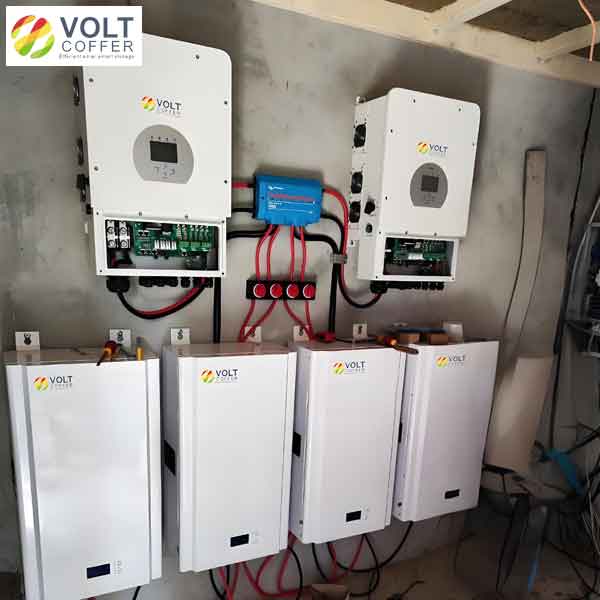
Future work in this domain will involve comprehensive loss modeling and efficiency comparisons between the FB7 and other advanced three-phase transformerless topologies (e.g., FB10, T-type with bypass) across a wide load range. Integration of this topology into hybrid or battery-integrated solar inverters, as hinted by system configurations combining inverters with LiFePO4 storage, presents a promising avenue for creating highly efficient and safe residential and commercial energy systems. The continued adoption of wide-bandgap power devices will further enhance the efficiency and power density of such innovative solar inverter designs, solidifying their role in the future renewable energy landscape.