
Renewable energy technologies are advancing at an unprecedented pace, and among them, perovskite solar cells have emerged as a promising candidate with remarkable potential. Over the past decade, the certified power conversion efficiency of perovskite solar cells has skyrocketed to 27.0%, a milestone that took crystalline silicon solar cells more than half a century to achieve. This rapid progress can be attributed to the unique advantages of perovskite materials, including their tunable composition and bandgap, abundant raw material sources, simple fabrication processes, and low production costs. Additionally, perovskite solar cells offer benefits such as lightweight flexibility and compatibility with silicon-based solar cells, further expanding their application potential and positioning them as a strong contender for next-generation mainstream photovoltaic technologies. In this article, I will delve into the fundamental physical principles, development history, structural classifications, optimization strategies, and various types of perovskite solar cells, followed by a discussion of their applications and future prospects.
The story of perovskite solar cells begins with the groundbreaking work on the photovoltaic effect, which was famously explained by Albert Einstein in 1905. He proposed the concept of photons as discrete particles of light, which carry energy and can liberate electrons from materials upon absorption. This principle underpins the operation of solar cells, where photons excite electrons in light-absorbing materials, and an internal electric field, such as that in a p-n junction, directs these electrons to generate electrical current. The standard testing conditions for solar cells, defined by the AM 1.5G spectrum with an incident energy density of 100 mW·cm⁻² and a temperature of 25 ± 1 °C, provide a benchmark for comparing the performance of different photovoltaic technologies, including perovskite solar cells.
Perovskite materials, named after the mineral calcium titanate (CaTiO₃), possess a general chemical formula of ABX₃, where A and B are cations of different sizes, and X is an anion. In the context of perovskite solar cells, metal halide perovskites are commonly used, with B sites occupied by divalent metal cations like Pb²⁺ or Sn²⁺, X sites by halide anions such as I⁻, Br⁻, or Cl⁻, and A sites by monovalent organic cations like methylammonium (MA⁺) or formamidinium (FA⁺) or inorganic cations like Cs⁺ or Rb⁺. The stability and formation of the perovskite structure are governed by the tolerance factor, t, defined as:
$$ t = \frac{R_A + R_X}{\sqrt{2} (R_B + R_X)} $$
where R_A, R_B, and R_X are the ionic radii of A, B, and X, respectively. A value of t close to 1 indicates a stable perovskite structure, typically between 0.8 and 1.0. The bandgap of metal halide perovskites, which ranges from 1.3 to 3.5 eV, is primarily influenced by the interaction between the p-orbitals of the B-site metal and X-site halide ions, allowing for flexible tuning through compositional engineering.
The inception of perovskite solar cells dates back to 2009, when Tsutomu Miyasaka and colleagues first used organic-inorganic hybrid lead halide perovskites, specifically MAPbX₃ (X = I or Br), as light absorbers in a dye-sensitized solar cell structure. Although the initial power conversion efficiency was modest at around 3.8%, and stability was poor, this work laid the foundation for future advancements. By 2012, significant breakthroughs were achieved independently by Henry J. Snaith and the team of Nam-Gyu Park and Michael Grätzel. They demonstrated all-solid-state perovskite solar cells with efficiencies exceeding 9-10%, utilizing mesoporous TiO₂ or insulating Al₂O₃ scaffolds and solid-state hole transport layers like Spiro-OMeTAD. These studies highlighted the dual role of perovskites as both light absorbers and charge transporters, thanks to their bipolar charge transport properties and long carrier diffusion lengths, as confirmed by transient spectroscopy studies.
Since then, the efficiency of perovskite solar cells has progressed rapidly, as summarized in Table 1, which compares the efficiency milestones of various photovoltaic technologies. This rapid advancement is a testament to the collaborative efforts of the global research community and the inherent advantages of perovskite materials.
| Technology | Year | Efficiency (%) |
|---|---|---|
| Perovskite Solar Cell | 2009 | 3.8 |
| Perovskite Solar Cell | 2012 | 10.9 |
| Perovskite Solar Cell | 2025 | 27.0 |
| Crystalline Silicon | 1954 | 6.0 |
| Crystalline Silicon | 2025 | 26.8 |
The device architecture of perovskite solar cells has evolved significantly, leading to various structures that can be broadly classified into mesoporous and planar configurations, as well as n-i-p (regular) and p-i-n (inverted) orientations. In mesoporous structures, which are derived from dye-sensitized solar cells, a mesoporous metal oxide layer (e.g., TiO₂ or Al₂�₃) serves as a scaffold for the perovskite layer, facilitating electron transport. The planar structures, on the other hand, eliminate the mesoporous layer, relying on the perovskite’s inherent charge transport properties. The n-i-p structure typically features an electron transport layer (e.g., TiO₂ or SnO₂) deposited on the transparent conductive oxide (TCO) substrate, followed by the perovskite layer and a hole transport layer (e.g., Spiro-OMeTAD or PTAA). In contrast, the p-i-n structure reverses this order, with a hole transport layer (e.g., PEDOT:PSS or NiOₓ) on the TCO substrate, followed by the perovskite and an electron transport layer (e.g., C₆₀ or PCBM). Table 2 provides a comparison of these structures, highlighting their advantages and challenges.
| Structure | Key Features | Advantages | Challenges |
|---|---|---|---|
| Mesoporous | Uses mesoporous scaffold (e.g., TiO₂) | Enhanced charge extraction | High-temperature processing |
| Planar n-i-p | Electron transport layer first | High efficiency, mature technology | Hysteresis effects |
| Planar p-i-n | Hole transport layer first | Low-temperature processing, good stability | Lower efficiency in early stages |
Interface engineering plays a crucial role in optimizing the performance of perovskite solar cells. The interfaces between the perovskite layer and charge transport layers are often sites of non-radiative recombination, which can limit device efficiency. Strategies such as surface passivation with organic ammonium salts (e.g., PEAI or guanidinium bromide) have been employed to reduce defect states and improve energy level alignment. For instance, treating the perovskite surface with PEAI has been shown to enhance open-circuit voltage and efficiency in n-i-p structures. Similarly, optimizing the buried interface—the interface between the perovskite and the underlying charge transport layer—has gained attention recently. Techniques like无损剥离 and confocal fluorescence imaging have revealed that the buried interface often exhibits greater heterogeneity and non-radiative recombination than the top interface. Molecular additives, such as bis(2-aminoethyl) ether (BAE), have been used to modify the buried interface, leading to significant improvements in efficiency and stability.
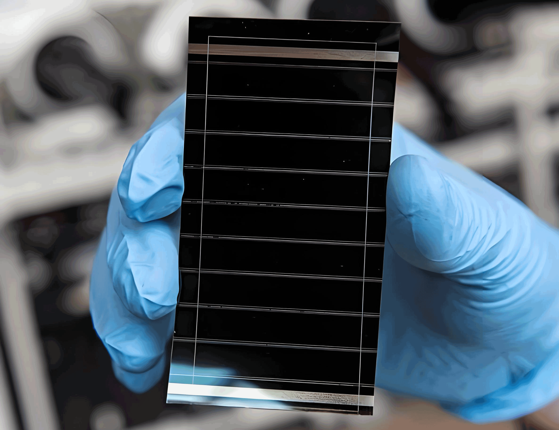
The fabrication of perovskite layers typically involves one-step or two-step solution processing methods. In the one-step method, a precursor solution containing lead halide (e.g., PbI₂) and organic ammonium halide (e.g., FAI) in solvents like DMF or DMSO is deposited onto the substrate, followed by anti-solvent dripping or vacuum flash evaporation to remove excess solvent and annealing to crystallize the perovskite. The two-step method involves first depositing a PbI₂ film, which is then converted to perovskite by exposure to an organic ammonium halide solution. The quality of the perovskite film, including grain size and coverage, is critical for device performance and can be influenced by factors such as precursor composition, solvent choice, and processing conditions.
To surpass the Shockley-Queisser (SQ) limit for single-junction solar cells, which is approximately 33.7% for perovskite solar cells, tandem or multi-junction configurations have been developed. These devices stack multiple sub-cells with different bandgaps to more efficiently utilize the solar spectrum. The theoretical efficiency of a tandem solar cell can be calculated based on the bandgaps of the sub-cells. For a two-junction tandem, the optimal bandgaps are around 1.1 eV for the bottom cell and 1.7 eV for the top cell, with a theoretical efficiency exceeding 40%. The efficiency η of a tandem cell can be expressed as:
$$ \eta = \frac{J_{sc} \times V_{oc} \times FF}{P_{in}} $$
where J_sc is the short-circuit current, V_oc is the open-circuit voltage, FF is the fill factor, and P_in is the incident power density. In two-terminal (2T) tandem cells, the sub-cells are connected in series, requiring current matching, whereas in four-terminal (4T) tandem cells, the sub-cells operate independently, allowing for more flexibility. Perovskite solar cells are particularly suitable for tandem applications due to their tunable bandgaps. For example, perovskite-silicon tandem cells have achieved efficiencies over 34%, while all-perovskite tandems have reached above 26%. Table 3 summarizes the progress in tandem perovskite solar cells.
| Tandem Type | Configuration | Efficiency (%) | Year |
|---|---|---|---|
| Perovskite-Silicon | 2-terminal | 34.6 | 2024 |
| All-Perovskite | 2-terminal | 26.4 | 2024 |
| Perovskite-CIGS | 2-terminal | 10.9 | 2015 |
| Perovskite-Organic | 2-terminal | 25.7 | 2024 |
Flexible perovskite solar cells represent another exciting frontier, leveraging the low-temperature processability and mechanical flexibility of perovskite materials. These devices are fabricated on flexible substrates such as PET, PEN, or polyimide, and they hold promise for applications in wearable electronics, building-integrated photovoltaics (BIPV), and space power systems. The key challenges include achieving high-quality perovskite films on flexible substrates and developing durable, conductive electrodes. Recent advances have led to flexible perovskite solar cells with efficiencies exceeding 24%, and their power-per-mass ratio has reached over 30 W·g⁻¹, significantly higher than traditional silicon or gallium arsenide solar cells. The performance of flexible perovskite solar cells can be summarized in Table 4.
| Substrate | Structure | Efficiency (%) | Power per Mass (W·g⁻¹) |
|---|---|---|---|
| PET/ITO | n-i-p | 16.8 | ~5 |
| PEN/ITO | p-i-n | 24.1 | ~10 |
| Parylene/InOₓ | p-i-n | 20.2 | 30.3 |
| Paper/Au | p-i-n | 2.7 | ~1 |
The applications of perovskite solar cells are diverse and expanding rapidly. In building-integrated photovoltaics (BIPV), semi-transparent and colored perovskite solar cells can be integrated into windows and facades. For automotive applications, lightweight perovskite solar cells on car roofs offer auxiliary power. In consumer electronics, flexible perovskite solar cells can power wearable devices and IoT sensors, thanks to their good performance under low-light conditions. Moreover, perovskite solar cells have shown potential for space applications due to their high radiation tolerance and excellent power-per-mass ratio. Large-scale ground-mounted power plants and distributed photovoltaic systems are also emerging as viable markets, with companies worldwide scaling up production. The versatility of perovskite solar cells is further enhanced by their ability to function in dual-mode devices, such as combined solar cells and light-emitting diodes, opening up possibilities for self-powered displays.
Despite the remarkable progress, several challenges remain for the widespread adoption of perovskite solar cells. Stability issues under operational conditions, such as exposure to moisture, oxygen, and light, need to be addressed through improved encapsulation and material design. The presence of lead in most high-efficiency perovskite solar cells raises environmental concerns, prompting research into lead-free alternatives like tin-based perovskites, though these often face efficiency and stability trade-offs. Scaling up from small-area devices to large modules while maintaining high efficiency is another critical hurdle, requiring advancements in coating techniques and uniformity control. Furthermore, a deeper understanding of the fundamental mechanisms, such as ion migration and degradation pathways, is essential for long-term reliability.
In conclusion, perovskite solar cells have demonstrated extraordinary growth in efficiency and versatility over a short period. Their future trajectory may involve competing directly with silicon solar cells, collaborating in tandem configurations, or pioneering niche applications where their unique properties shine. As research continues to tackle stability, scalability, and environmental issues, perovskite solar cells are poised to play a significant role in the global transition to sustainable energy. The journey of perovskite solar cells is a testament to innovation and collaboration, and I am optimistic that they will continue to break new ground in the years to come.
To quantify the impact of various optimization strategies on perovskite solar cell performance, consider the following empirical relationship for efficiency improvement based on defect passivation and interface engineering:
$$ \eta = \eta_0 + \Delta \eta_{\text{passivation}} + \Delta \eta_{\text{interface}} $$
where η₀ is the baseline efficiency, Δη_passivation represents the gain from reducing non-radiative recombination, and Δη_interface accounts for improvements in charge extraction. Studies have shown that effective passivation can reduce voltage losses by up to 100 mV, leading to efficiency boosts of 2-3%. As the field advances, the integration of machine learning and high-throughput experimentation may accelerate the discovery of optimal materials and processes for perovskite solar cells, further solidifying their position in the photovoltaic landscape.