
The performance of solar inverters can be intuitively evaluated through their key output waveforms, such as the output waveform of the inverter half wave, the voltage waveform of the clamp capacitor, the soft switching control waveform, the drain source voltage and driving voltage waveform of the power switching transistor, the output waveform of the dual alternating half wave, the dynamic MPPT test waveform, and the output waveform of the inverter full wave. After modifying, optimizing, and innovating the main technical shortcomings of each part of the original solar inverter and the problems encountered during the experimental process, the collected main output waveforms will be compared and analyzed with the output waveforms of the original solar inverter.
Based on the shortcomings and deficiencies in the main technologies of each link in the design of solar inverters, a design plan is formulated to gradually improve the overall performance and efficiency of solar micro inverters by correcting and improving related technologies. By collecting waveforms before and after the design and conducting corresponding comparative analysis and relevant mathematical theoretical derivation verification, it can be fully demonstrated that the proposed innovative design strategy and method optimize the inverter strategy of traditional solar inverters, and have significant improvements and performance improvements in improving the inverter efficiency and stability of solar inverters.
1. Comparison of output waveforms of improved half wave circuits
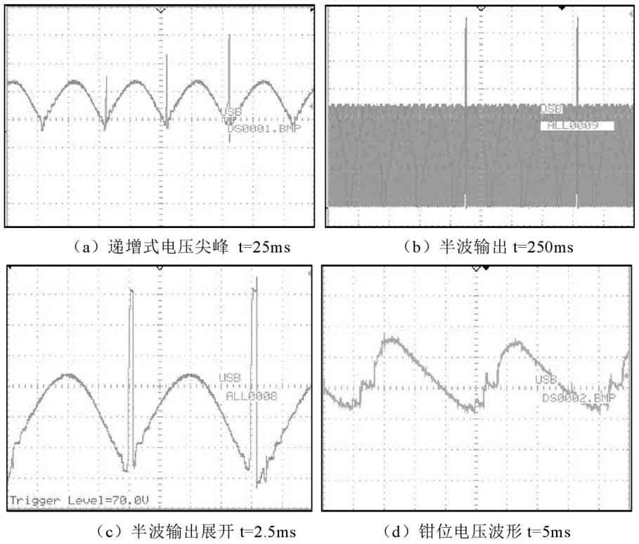
According to the analysis of the absorption of leakage inductance energy and the discharge of Coss capacitor during the conduction and shutdown process of power switching tubes, it can be concluded that if the output circuit of the DC-DC link of the solar inverter is not equipped with a reasonable current absorption circuit for leakage inductance energy feedback and reuse, the leakage inductance energy will continuously accumulate on the original side of the transformer, showing an increasing or sudden waveform distortion phenomenon with an amplitude of about 70V peak. Figure 1 shows the relevant waveform of the half wave output of the solar inverter before the modification of the half wave circuit. Figure 1 (a) captures the phenomenon of leakage inductance energy accumulation. It can be clearly seen from the figure that there is almost equivalent leakage inductance energy accumulation in each cycle, and after reaching a certain voltage value, the leakage inductance energy forms a back impact on the power switch tube, releasing energy. Figure 1 (b) is the half wave rectification waveform, Figure 1 (c) shows the expansion of the half wave rectification waveform. From the oscilloscope display, it can also be seen that there is a peak voltage of 70V in the half wave waveform and energy jitter at the half wave connection caused by energy loss. Figure 1 (d) shows the clamp voltage waveform before modification. According to the theoretical derivation of circuit parameters, the clamp voltage waveform indicates that there is a mismatch in the current circuit design and parameter selection.
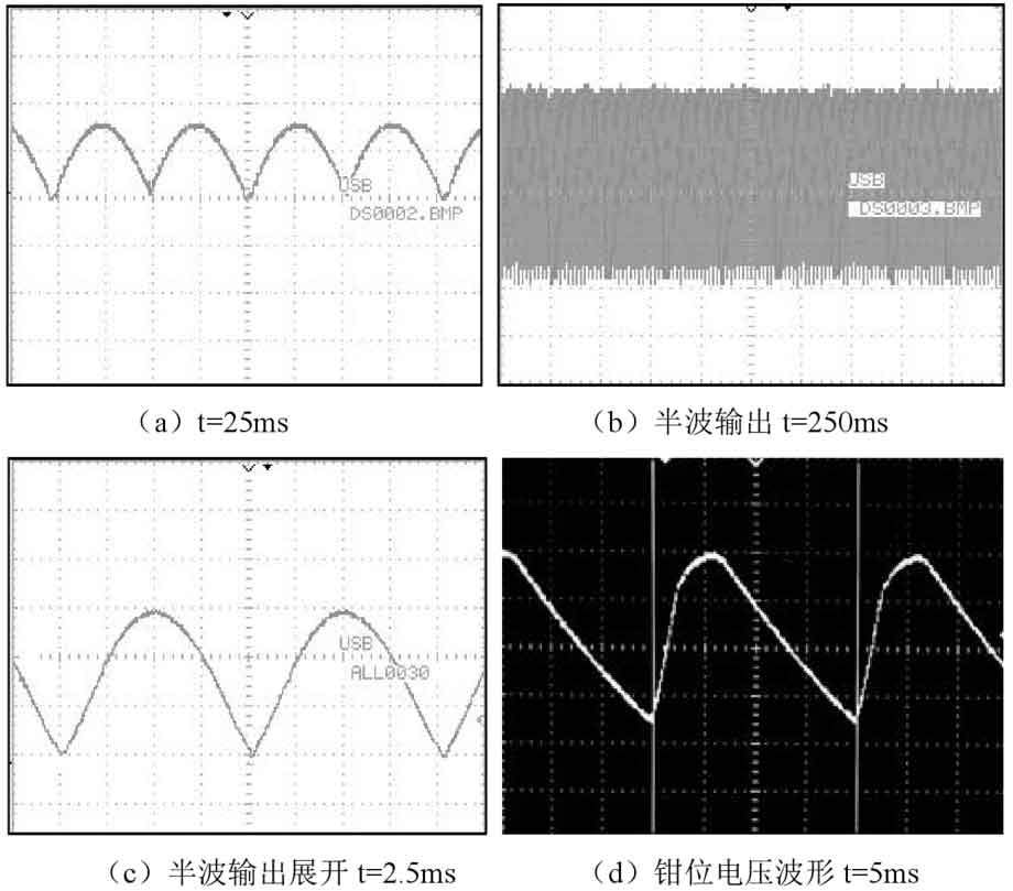
In order to fully utilize excess leakage inductance energy and suppress the impact of peak voltage caused by parasitic capacitance discharge of power switching tubes, corresponding energy absorption and peak suppression circuits are proposed to construct a circuit to discharge leakage inductance energy and peak energy, and re input the energy to the input end. After the next cycle arrives, it is used for backup again. A key factor in the design of this circuit is the selection of circuit parameters. According to different production needs, it is necessary to derive formulas based on theory and re derive the selection of circuit parameters. After using the parameters derived from theory in the circuit, the half wave output waveform no longer contains energy jitter, energy loss caused by peak voltage, and waveform distortion. The half wave output waveform of the improved RCD leakage inductance energy absorption and voltage spike suppression circuit is shown in Figure 2. Figure 2 (a) shows the capture experiment of the peak voltage superposition phenomenon under the same conditions. From the actual experimental waveform, it can be seen that the gradually stacked peak voltage phenomenon is eliminated. Figures 2 (b) and 2 (c) show the expansion of the half wave rectification output waveform and the half wave rectification output waveform under the same conditions. It can be seen that the peak voltage of about 70V caused by the reverse impact of leakage inductance energy and Coss capacitor discharge is eliminated, And the waveform jitter phenomenon at the half wave connection caused by energy loss has also been corrected. Figure 2 (d) shows the clamp capacitor voltage waveform of the modified half wave output circuit derived based on circuit parameter theory. It can be seen from the figure that the clamp voltage waveform is stable and smooth, close to the ideal clamp waveform.
2. Comparison of output waveforms of improved MPPT algorithm control strategy
The essence of MPPT technology is an algorithm for finding the optimal peak value. The measurement of this algorithm cannot be limited to a certain waveform, but is evaluated through the final full wave inverter waveform and dynamic MPPT efficiency. Since the IV curve of the solar inverter input is constantly changing according to load matching, the IV curve at one moment and the IV curve at the next moment are two different output curves, and there is no correlation between the output power at each moment.
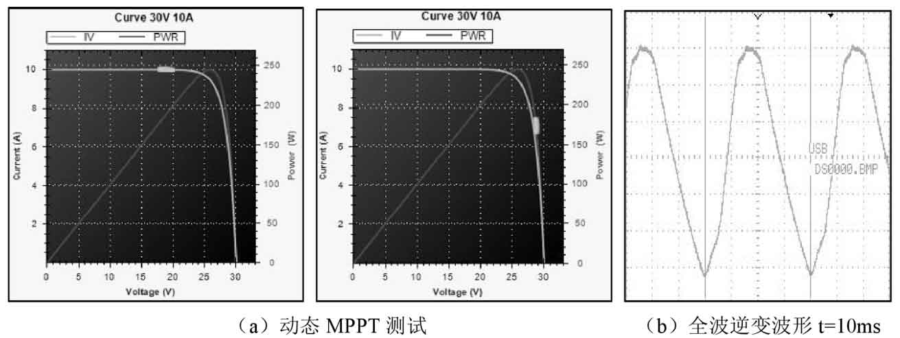
According to the analysis of the traditional MPPT algorithm, the fixed voltage control algorithm can only limit the output power corresponding to one output voltage value. When the maximum power point corresponding to the actual input does not meet the set output power, there will be a left or right shift of the power point as shown in Figure 3 (a), resulting in a deficit in output power. Similarly, for the disturbance voltage control algorithm, because it is essentially an active interference, the maximum power point matching is carried out based on the output power corresponding to the output voltage after interference. When the disturbance factor is not set properly or in the early stage of disturbance adjustment, there will be a rapid oscillation of the current power point between the left and right power points shown in the figure, causing the output voltage to be intermittent and unstable, The efficiency of dynamic MPPT is less than 95% and cannot be stably displayed. Figure 3 (b) shows the full wave inverter waveform during low-power output due to incorrect MPPT algorithm. As can be seen from the figure, the waveform degradation process and waveform distortion at the downstream peak are severe, and it no longer possesses sinusoidal output characteristics.
In order to meet the design requirements of maximum power tracking and stabilize the continuous output voltage at the maximum power point, a power variable step size MPPT control strategy combining the advantages of fixed voltage, disturbance observation, and traditional variable step size conductance increment method is proposed. Based on mathematical formulas and combined with the proposed control strategy flow, the circuit topology can be greatly optimized, hardware calculation steps can be simplified, and maximum power point tracking efficiency and maximum power point output efficiency can be provided.
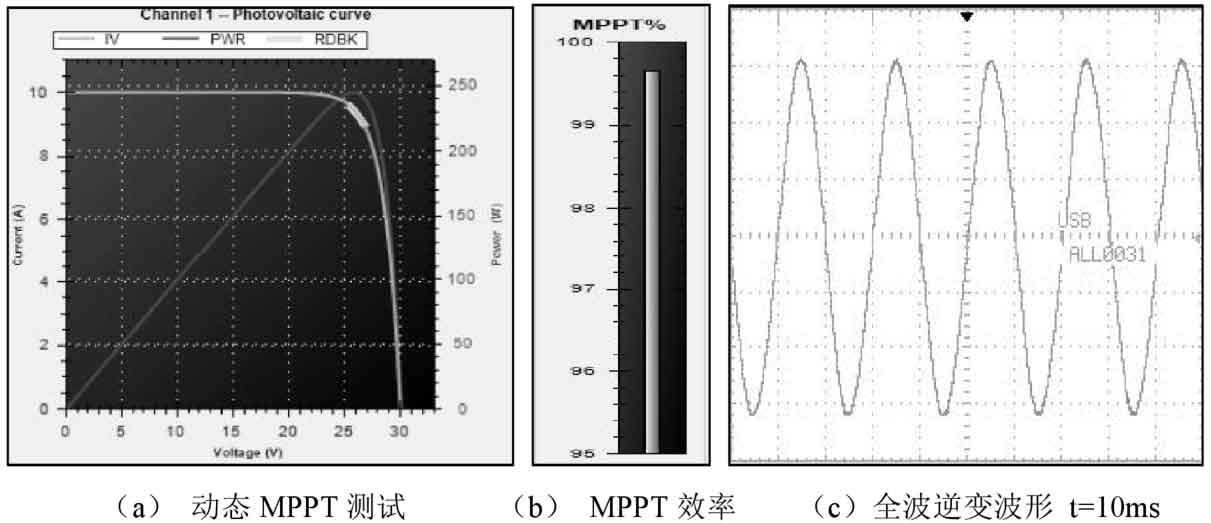
The power output waveform and inverter full wave of the solar inverter after adding the MPPT control algorithm based on power variable step size and combining the advantages of fixed voltage, disturbance observation, and traditional variable step size conductance increment are shown in Figure 4. Among them, Figure 4 (a) and Figure 4 (b) show the output waveform of the solar inverter power point and the dynamic MPPT efficiency test. It can be seen that the power point stays near the maximum power, and its corresponding dynamic MPPT efficiency is 99.62%, with a deviation of ± 0.02%. Figure 4 (c) shows the AC sine full wave output under this condition, with a voltage waveform that conforms to sinusoidal characteristics and is very smooth.
Under the same experimental testing conditions, the modified inverter efficiency increased from around 80% to around 92% compared to the previous one. The solar inverter achieved stable output at the maximum power point, and the overall performance and inverter efficiency of the solar inverter were significantly improved.
3. Comparison of output waveforms of improved peak voltage suppression and soft switching control strategies
Soft switching technology is essential in the design of solar micro inverters. Implementing soft switching technology can not only solve the switching loss problem of power switching tubes in high-frequency operating conditions, but more importantly, it provides a guarantee for the stable and safe operation of solar micro inverters. Although soft switching technology has become relatively mature, and mathematical formulas and theoretical derivations have been applied to the design of related soft switching algorithms, based on the introduction of soft switching technology, it can be known that the success of soft switching technology depends on whether it can achieve zero voltage conduction. Through the analysis of principles and practical experimental phenomena, control strategies based on traditional soft switching formulas are proposed, Although there is some improvement in its effectiveness in achieving zero voltage conduction, it is not significant. The waveform is shown in Figure 5 (a), and it can be seen that when the drain source voltage of the power switching transistor drops to zero, the driving voltage starts to rise from zero, and the delay time between them is too short or not significant.
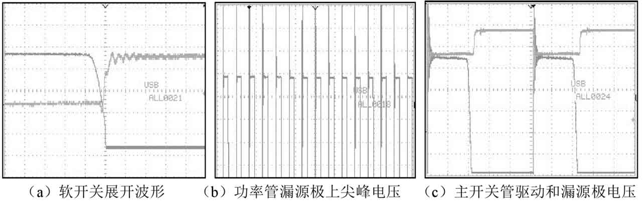
In addition, from the perspective of circuit topology structure, in order to make the designed circuit topology simple and not complex, transformer parasitic capacitance and drain source capacitance are usually selected for resonance to achieve soft switching control strategy. However, the voltage spike phenomenon caused by resonance will result in a high amplitude spike voltage pulse in each switching cycle, as shown in Figure 5 (b), which poses a great threat to the safety of power switching tubes. Figure 5 (c) shows the development of this spike voltage phenomenon.
In order to make the soft switching phenomenon more prominent and suppress the peak voltage caused by resonance, a soft switching control strategy based on PI method is proposed to suppress the peak voltage. By setting up a PI controller and taking the actual input voltage at the current moment as the expected value, the output voltage is collected and compared with the expected value to correct the peak voltage phenomenon caused by the deviation formed by the comparison, gradually approaching the expected value in the near future. At the same time, when designing the soft switching algorithm, the theoretical derivation process of the MPPT algorithm was fully integrated, and the mathematical formula of the soft switching was extended and modified.
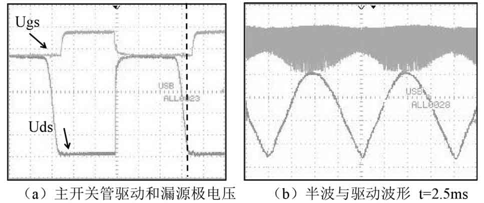
The driving waveform and drain source waveform of the power switching transistor after adding a soft switching control strategy based on PI method to suppress peak voltage, as well as the driving waveform and half wave waveform, are shown in Figure 6. It can be clearly seen from Figure 6 (a) that the peak voltage caused by transformer parasitic capacitance and power switch parasitic capacitance resonance is effectively suppressed. In each cycle, the driving voltage only rises from zero after the drain source voltage drops to zero. The soft switching algorithm based on PI method to suppress peak voltage highlights the phenomenon of zero voltage conduction.
4. Comparison of output waveforms of improved full wave inverter circuit
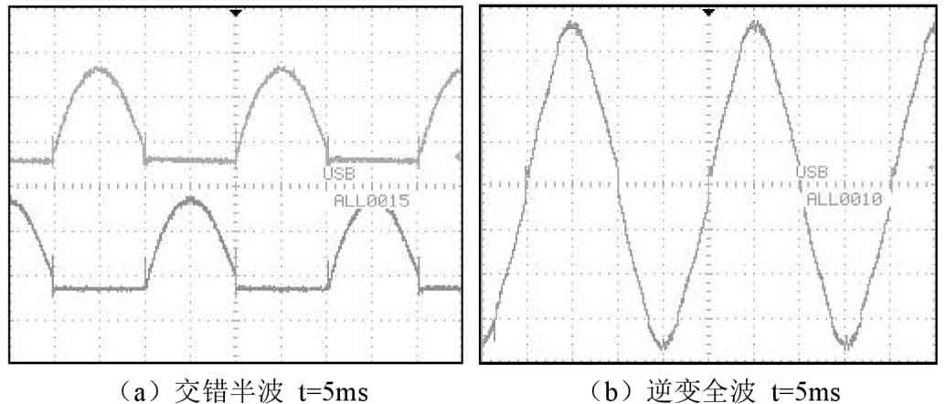
According to the analysis, the full wave inverter section outputs a power frequency sine wave based on the first two parts, but due to the setting of the dead time, there is often a phenomenon of zero point drop. Figures 7 (a) and 7 (b) show the inverter output waveforms before correcting the full wave inverter circuit. Among them, Figure 7 (a) shows the interleaved dual half wave output waveform. From the measured waveform, it can be seen that during the process of the lower half wave dropping from the peak to zero, it has not yet dropped to zero, and the upper half wave has started to rise from zero to the peak. Moreover, traditional H-bridges do not have zero crossing detection capability, This causes a hard cutoff at each half wave zero crossing, resulting in a small spike pulse. The full wave waveform of the interleaved dual half wave output by the H-bridge inverter circuit is shown in Figure 7 (b). From the figure, it can be clearly seen that there is a feeling of drop at the zero crossing position of the sine wave, which makes the inverted full wave a quasi sine wave, seriously affecting the quality of the inverter output waveform.
In order to solve the problems of traditional H-bridge not having zero point detection capability and full wave zero point drop and phase shift caused by abnormal cutoff of the generated dual interleaved half wave, a synchronous inverter control strategy based on controllable silicon H-bridge inverter circuit combined with external interrupt algorithm is proposed. By utilizing the characteristics of thyristor zero cutoff, zero crossing detection is performed from a circuit perspective. At zero, an external interrupt algorithm is triggered, and zero crossing detection is performed again from a software algorithm. The half wave generated by the duty cycle of the power switch is controlled for zero crossing calibration, ensuring good separation of the output dual interleaved half waves.
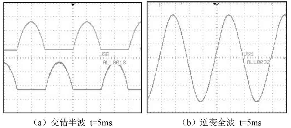
Figure 8 shows the output waveform of the inverter with the addition of an H-bridge inverter circuit based on thyristors and an external interrupt calculation for synchronous inverter control strategy. It can be seen that the upper and lower half waves are reduced to zero before the other waveform begins to output. The burrs at the zero crossing of each half wave are also eliminated, and the phase shift of the half wave and the voltage drop of the sine full wave at the zero point of the inverter are corrected.