
As an industry analyst closely tracking the evolution of advanced materials and energy technologies, I often encounter a flood of market rumors and speculative reports. The recent circulation of two specific claims regarding supply chain relationships in the battery and solar sectors serves as a perfect case study on the critical need for rigorous verification and the dangers of information asymmetry. This analysis will delve into the technological context behind these rumors, dissect the factual corrections provided, and expand into a broader discussion on the materials science and market dynamics at play, with a particular focus on the transformative potential of thin film solar panel technology.
The first rumor suggested a singular, exclusive supplier relationship for a critical battery component. The second pertained to the operational management of a new manufacturing venture. Both were promptly addressed by the companies involved, highlighting a common narrative where partial truths are extended into definitive, but inaccurate, conclusions. This pattern underscores a market thirst for simple narratives in complex, interconnected technological ecosystems.
At the heart of the first correction lies a fundamental challenge in electrochemistry: fast-charging lithium-ion batteries. The bottleneck is primarily at the anode, typically composed of graphite. During rapid lithium-ion intercalation, standard graphite structures can lead to undesirable side reactions, including lithium plating—a dangerous condition where lithium ions are deposited on the surface instead of being smoothly inserted into the graphite lattice. This compromises cycle life, stability, and safety. The solution, as referenced in the rumors, involves sophisticated engineering of the graphite particles. Techniques like creating a “fast ion ring” or constructing a hierarchical pore and surface structure aim to build a “highway network” for lithium ions, facilitating rapid and uniform embedding. This can be conceptually modeled by modifying the classic diffusion equation to account for enhanced surface pathways. The lithium ion diffusion can be described by Fick’s law, but the engineered interface creates a preferential flux. One can think of the total flux \( J_{total} \) into a graphite particle as:
$$ J_{total} = J_{bulk} + J_{surface} = -D_{bulk} \nabla c + \kappa A_{surface} (c_{ext} – c_{int}) $$
Here, \( D_{bulk} \) is the bulk diffusion coefficient, \( \nabla c \) is the concentration gradient, \( \kappa \) is a surface permeability constant enhanced by the “fast ion ring” treatment, \( A_{surface} \) is the effective surface area, and \( c_{ext} \) and \( c_{int} \) are the external and interface lithium concentrations. The innovation lies in maximizing \( \kappa A_{surface} \), ensuring ions are quickly distributed across the surface and then into the bulk, preventing localized saturation and plating.
The confirmation that a company’s subsidiary is a supplier, but not the sole supplier, into a leading battery manufacturer’s chain is significant. It speaks to the multi-sourcing strategies essential for scale and risk mitigation in high-growth industries. The move from a position of simple graphitization processing to producing “high-end anode materials” represents a classic attempt at vertical integration and value capture within the battery materials supply chain.
The second rumor shifts our focus to the solar energy sector, specifically the promising domain of thin film photovoltaic technology. The assertion was that a company was already operating a production line for Copper Indium Gallium Selenide (CIGS) thin film solar panels. The official clarification was clear: while the company has a stake in the joint venture and a right of first refusal for future operational management, the project is still under construction. No operational management is currently in place.
This leads us to a deep exploration of why CIGS thin film solar panel technology generates such interest and speculation. Unlike dominant crystalline silicon panels, thin film solar panels are created by depositing photovoltaic active layers, mere microns thick, onto substrates like glass, metal, or plastic. The CIGS variant is particularly noted for its high efficiency potential, flexibility, lightweight properties, and good performance in low-light conditions. The fundamental efficiency \( \eta \) of a solar cell is given by:
$$ \eta = \frac{P_{max}}{P_{in}} \times 100\% = \frac{J_{sc} \times V_{oc} \times FF}{P_{in}} \times 100\% $$
where \( P_{max} \) is the maximum power output, \( P_{in} \) is the incident solar power, \( J_{sc} \) is the short-circuit current density, \( V_{oc} \) is the open-circuit voltage, and \( FF \) is the fill factor. CIGS cells have achieved laboratory efficiencies exceeding 23%, rivaling polycrystalline silicon. Their bandgap can be tuned by adjusting the Gallium to Indium ratio \( \left( \frac{Ga}{In+Ga} \right) \), optimizing absorption across the solar spectrum:
$$ E_g^{CIGS}(x) \approx E_g^{CIS} + (E_g^{CGS} – E_g^{CIS})x – bx(1-x) $$
where \( x \) is the Gallium ratio, \( E_g^{CIS} \approx 1.04 \, eV \) for CuInSe₂, \( E_g^{CGS} \approx 1.68 \, eV \) for CuGaSe₂, and \( b \) is a bowing parameter.
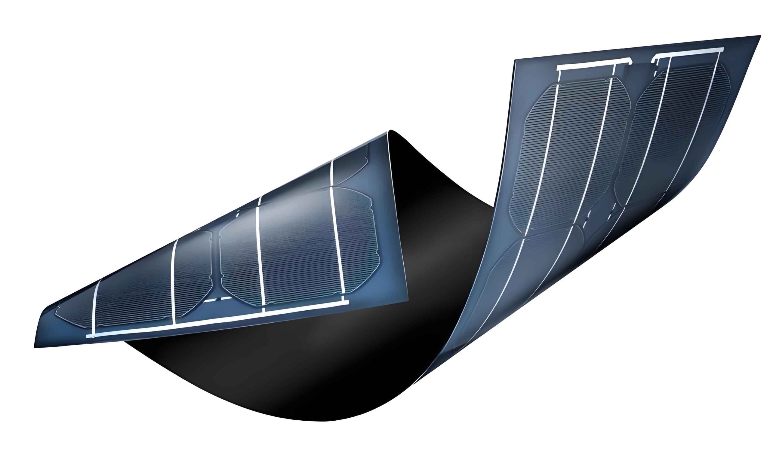
The visual above showcases the sleek, uniform appearance of a thin film solar panel array, highlighting its potential for building-integrated photovoltaics (BIPV) and other aesthetic applications. The business rationale for the joint venture, as stated, is clear: it allows partners to pool distinct competencies—core vacuum deposition and patterning工艺 from a display technology expert, proprietary efficiency-enhancing专利 from a research institute, and project engineering experience from an energy-focused firm. This synergy is intended to accelerate the challenging path from laboratory innovation to cost-competitive, gigawatt-scale manufacturing of thin film solar panels.
The following table summarizes the key competitive landscape for thin film solar panel technologies against the incumbent crystalline silicon (c-Si):
| Technology | Typical Lab Efficiency | Commercial Module Efficiency | Key Advantages | Key Challenges | Primary Substrates |
|---|---|---|---|---|---|
| Crystalline Silicon (c-Si) | >26% (Mono) | 19-22% | High efficiency, stable, abundant material, long history | Rigid, heavy, high material use & cost, efficiency drops at high temp | Silicon wafers |
| CIGS Thin Film | >23% | 15-18% | High efficiency potential, flexible/lightweight, good low-light performance, tunable bandgap | Complex fabrication, scarcity of In, long-term stability scaling | Glass, metal foil, polymer |
| CdTe Thin Film | >22% | 17-19% | Low-cost manufacturing, fast energy payback, stable | Toxicity of Cd, scarcity of Te | Glass |
| Perovskite Thin Film | >25% | ~18% (small module) | Rapid efficiency gains, very low-cost solution processing, lightweight | Severe stability issues, lead content, scaling challenges | Glass, flexible substrates |
The market for thin film solar panels is driven by several factors beyond pure efficiency. The levelized cost of electricity (LCOE) is the ultimate metric, given by:
$$ LCOE = \frac{\sum_{t=1}^{n} \frac{I_t + O_t + F_t}{(1+r)^t}}{\sum_{t=1}^{n} \frac{E_t}{(1+r)^t}} $$
where \( I_t \) is investment costs, \( O_t \) is operations & maintenance, \( F_t \) is fuel costs (zero for solar), \( E_t \) is energy produced, \( r \) is the discount rate, and \( n \) is the project lifetime. Thin film solar panels can lower \( I_t \) through simpler, roll-to-roll manufacturing and lower balance-of-system costs (e.g., lighter support structures). Their better temperature coefficient (less efficiency loss per degree Celsius of temperature increase) and superior diffuse light performance can increase \( E_t \) in certain climates, positively impacting LCOE.
Building on the technological promise, let’s analyze the broader market drivers and challenges for thin film solar panel adoption.
| Market Driver | Impact on Thin Film Solar Panel Demand | Quantitative Example / Metric |
|---|---|---|
| Building-Integrated PV (BIPV) | High. Flexibility and aesthetics make thin film ideal for roofs, facades, and windows. | BIPV market projected CAGR >15%. Thin film can command a price premium for architectural integration. |
| Portable & Off-Grid Electronics | Moderate-High. Lightweight and flexible form factors are crucial. | Demand for portable power for IoT, sensors, and consumer devices. Power-per-weight ratio is key. |
| Utility-Scale in Hot Climates | Moderate. Superior temperature coefficient improves yield relative to c-Si. | c-Si power loss ~0.4-0.5%/°C; CIGS/CdTe loss ~0.2-0.3%/°C. This can lead to 5-10% more annual energy in hot deserts. |
| Agrivoltaics & Lightweight Structures | Moderate. Semi-transparency and lightweight allow dual land use. | Thin film panels can be installed on structures that cannot bear heavy c-Si arrays. |
| Supply Chain Diversification | Strategic. Offers an alternative to silicon-dominated supply chains. | Reduces geopolitical and pricing risks associated with polysilicon production concentration. |
However, scaling production presents immense technical hurdles. The core challenge in manufacturing a high-efficiency CIGS thin film solar panel lies in controlling the complex quaternary compound’s stoichiometry and grain structure uniformly over large areas. The deposition process often involves co-evaporation or selenization/sulfurization of metallic precursors. Key parameters that must be controlled include:
1. Elemental ratios: \( \frac{Cu}{In+Ga} \) (CGI ratio) and \( \frac{Ga}{In+Ga} \) (GGI ratio) must be kept within narrow windows.
2. Sodium doping: Intentional incorporation of Na, often from the soda-lime glass substrate, improves grain growth and conductivity.
3. Bandgap grading: Engineering a depth-dependent Ga profile to create a back-surface field and improve \( V_{oc} \).
The quantum efficiency \( QE(\lambda) \), which measures the fraction of incident photons of wavelength \( \lambda \) that generate charge carriers, is acutely sensitive to these factors:
$$ QE(\lambda) = \frac{N_{e}}{N_{ph}(\lambda)} = (1-R(\lambda)) \cdot (1 – e^{-\alpha(\lambda) \cdot d}) \cdot \eta_{coll} $$
where \( R \) is reflectance, \( \alpha \) is absorption coefficient, \( d \) is absorber layer thickness, and \( \eta_{coll} \) is the charge collection efficiency. Poor morphology or incorrect stoichiometry directly reduces \( \alpha \) and \( \eta_{coll} \), lowering \( J_{sc} \) and thus the final module power output.
Beyond initial efficiency, long-term stability is paramount. The degradation of a thin film solar panel often follows a dual- or multi-stage model, distinct from c-Si. An empirical model for power loss over time \( t \) can be:
$$ P(t) = P_0 \cdot (1 – \delta_{LID} \cdot (1 – e^{-t/\tau_{LID}})) \cdot (1 – \beta \cdot t) $$
Here, \( P_0 \) is initial power, \( \delta_{LID} \) is the amplitude of light-induced degradation (often related to metastable defects in thin films), \( \tau_{LID} \) is its time constant, and \( \beta \) is a constant rate of degradation from other mechanisms (e.g., moisture ingress, electrode corrosion). Encapsulation to prevent moisture and oxygen penetration is even more critical for many thin film solar panel technologies than for c-Si.
| Technical Challenge | Impact on Module | Current Mitigation Strategies |
|---|---|---|
| Uniform Large-Area Deposition | Directly impacts yield, efficiency distribution, and manufacturing cost per watt. | Advanced spatial monitoring and dynamic process control during co-evaporation; improved precursor ink formulations for printing. |
| Defect Passivation | High defect density at grain boundaries reduces \( V_{oc} \) and \( FF \). | Alkali post-deposition treatments (PDT) with Na, K, Rb; alloying with Ag or S. |
| Transparent Conductive Oxide (TCO) Front Contact | Must balance high conductivity, high transparency, and stability under damp heat. | Development of doped zinc oxide (ZnO:Al, ZnO:B) and improved indium tin oxide (ITO) to reduce indium use. |
| Back Contact Stability | Molybdenum (Mo) back contact can form resistive MoSe₂ layer; delamination risks. | Engineering the Mo deposition parameters and the CIGS/Mo interface through controlled selenization. |
| Encapsulation & Long-Term Reliability | Moisture-induced corrosion and performance decay. IEC 61215/61646 testing is mandatory. | Robust edge sealing, high-performance barrier films (for flexible panels), and stable, UV-resistant encapsulants like ionomers. |
From an investment and strategic perspective, the rumors and their clarifications highlight a framework for evaluating companies in this space. The value lies not in a binary “yes/no” to a specific rumor, but in assessing a company’s position on a technology readiness and integration spectrum. We can propose a simplified scoring metric for a firm’s position in the advanced thin film solar panel value chain:
$$ TRI = \sum_{i=1}^{n} w_i \cdot S_i $$
where \( TRI \) is the Technology Readiness & Integration score, \( w_i \) is the weight for category \( i \), and \( S_i \) is the score (0-10) for that category. Categories include:
– \( R\&D \) Capability (Patents, Lab Efficiency)
– \( Pilot \) Production Scale & Yield
– \( Strategic \) Partnerships & JV Structure
– \( Supply \) Chain Access for Critical Materials (In, Ga, Se)
– \( Downstream \) Market Access (BIPV, Utility Projects)
– \( Financial \) Capacity for Gigawatt-Scale Capex
A company merely holding a non-controlling stake in a JV during the construction phase (as clarified in the second rumor) would score highly in “Strategic Partnerships” but low in “Pilot Production” and “Downstream Market Access.” Its future value is contingent on successfully transitioning across these categories.
Furthermore, the lifecycle of such a project can be modeled in phases, each with distinct risk and capital expenditure (CapEx) profiles. The initial research and pilot phase requires high CapEx for specialized equipment with significant technical risk. The commercial scaling phase sees CapEx peak for factory build-out, with risk shifting towards operational efficiency and market acceptance. Finally, the maturity phase focuses on optimizing OpEx and incremental technology improvements. The net present value (NPV) of such a venture is highly sensitive to the learning curve—the rate at which manufacturing cost decreases with cumulative production volume, often modeled by Wright’s Law:
$$ C_N = C_1 \cdot N^{-b} $$
where \( C_N \) is the cost of the \( N \)-th unit, \( C_1 \) is the cost of the first unit, and \( b \) is the learning coefficient (a larger \( b \) means faster cost reduction). For a capital-intensive, nascent technology like advanced thin film solar panel manufacturing, achieving a steep learning curve is existential.
In conclusion, the dissection of market rumors serves as a gateway to understanding the profound technical and commercial complexities in sectors like advanced batteries and next-generation photovoltaics. The key takeaway is the paramount importance of verification and contextualization. A company’s entry into a supply chain is a milestone, not a guarantee of dominance. An investment in a joint venture developing CIGS thin film solar panel technology is a strategic option on a future capability, not evidence of current revenue streams. The real story is always in the intricate details of materials science, process engineering, supply chain logistics, and the relentless pursuit of scaling laws. As both the battery and solar industries continue their rapid evolution, driven by the global energy transition, stakeholders must cultivate a disciplined focus on these underlying fundamentals rather than the noise of the rumor mill. The future belongs to technologies that can navigate the valley of death between lab-scale promise and cost-competitive, reliable manufacturing at scale—a journey where every claim must be rigorously validated against physical and economic reality.