
The global pursuit of sustainable energy solutions has placed solar power at the forefront of technological innovation. Amidst this shift, the paradigm is gradually moving beyond traditional, rigid photovoltaic modules towards more versatile and integrable forms. Among these, compound semiconductor thin film solar panels represent a transformative technology, offering a compelling combination of efficiency, low-cost manufacturing potential, and unprecedented physical flexibility. These panels, fabricated by depositing micrometer-thin layers of light-absorbing materials onto flexible substrates like polymers or metal foils, are redefining where and how solar energy can be harnessed.
The fundamental appeal of the thin film solar panel lies in its material economy and process scalability. Compared to conventional wafer-based silicon cells, thin film technologies consume significantly fewer raw materials—often by orders of magnitude. This is succinctly captured by the ratio of material thickness to absorption capability, characterized by the absorption coefficient α(λ). For direct bandgap semiconductors common in thin films, α(λ) is high (>104 cm-1), allowing near-complete light absorption within 1-2 μm. The amount of active material required per panel, M, can be approximated as:
$$M = \rho \cdot d \cdot A$$
where ρ is the material density, d is the optimal absorber layer thickness (typically 1-3 μm for thin films vs. 150-200 μm for silicon), and A is the panel area. This drastic reduction in d is the primary driver for lower material cost and energy payback time for thin film solar panels.
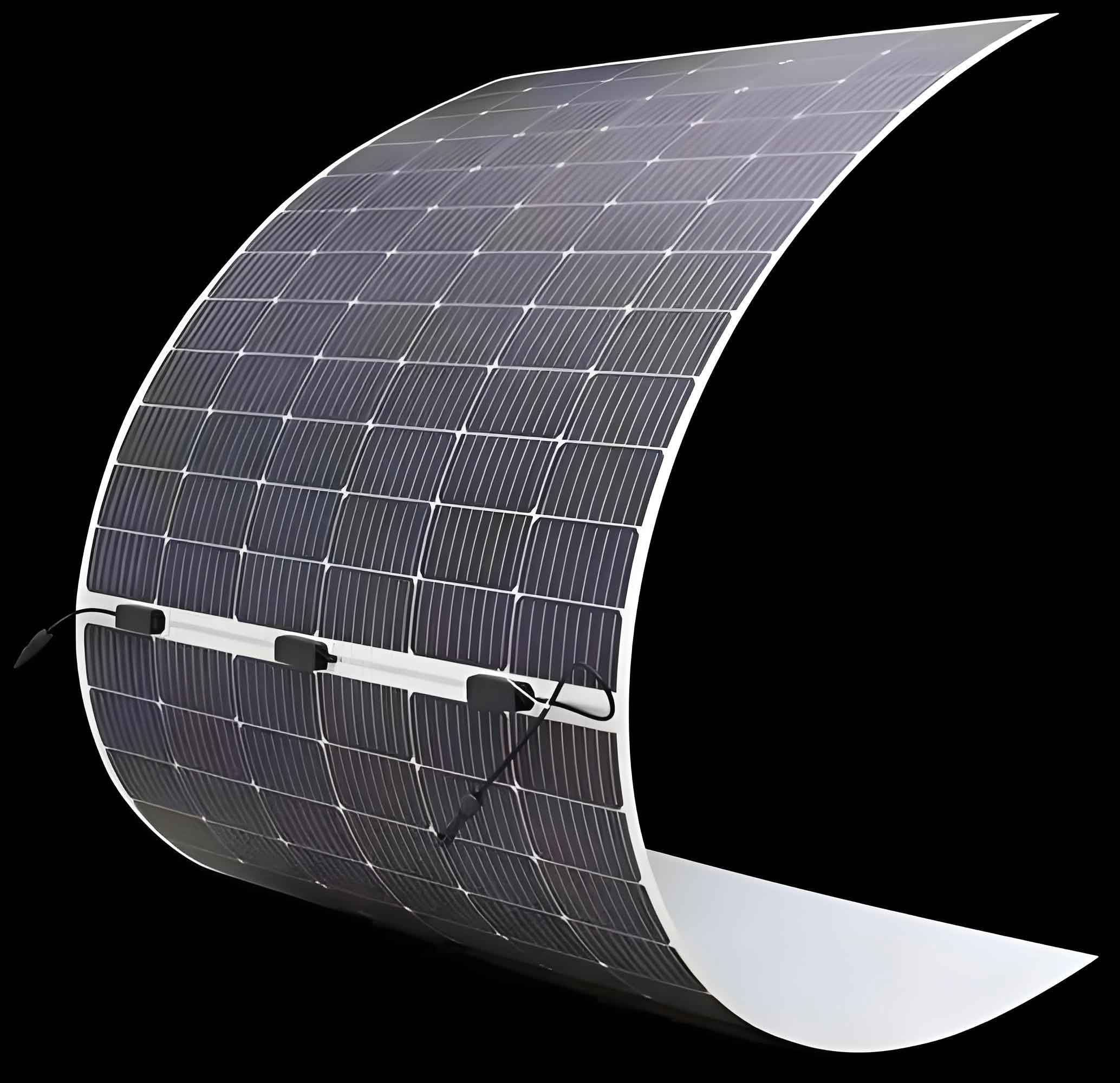
Furthermore, the manufacturing of flexible thin film solar panels is compatible with continuous roll-to-roll (R2R) processing, a high-throughput, low-energy technique analogous to printing newspapers. This contrasts with the batch processing of silicon ingots and wafers. The potential for low-temperature deposition on lightweight, flexible substrates unlocks applications impossible for rigid glass modules: building-integrated photovoltaics (BIPV) on curved surfaces, portable power for electronic devices, vehicle-integrated solar, and large-scale deployments on lightweight structures. The mechanical flexibility is often quantified by the minimum bending radius Rmin before efficiency degradation, which is related to the substrate and layer stack’s tensile strain ε:
$$R_{min} = \frac{t_{substrate}}{2\varepsilon_{critical}}$$
where tsubstrate is the substrate thickness and εcritical is the maximum strain the semiconductor layer can withstand. Advanced thin film solar panels on polymer substrates can achieve Rmin values of just a few millimeters.
Operational Principles and Efficiency Metrics
At its core, a thin film solar panel operates on the principle of the photovoltaic effect within a semiconductor p-n junction. When photons with energy greater than the semiconductor’s bandgap (Eg) strike the absorber layer, they excite electrons from the valence band to the conduction band, creating electron-hole pairs (EHPs). The built-in electric field at the p-n junction then separates these charges, driving electrons toward the n-type layer and holes toward the p-type layer, thereby generating a photocurrent.
The performance of a thin film solar panel is evaluated by several key parameters under standard test conditions (STC: AM1.5G spectrum, 1000 W/m², 25°C):
- Open-Circuit Voltage (VOC): The maximum voltage available from the panel at zero current. It is fundamentally limited by the bandgap and interface quality: $$V_{OC} \approx \frac{E_g}{q} – \frac{n k T}{q} \ln\left(\frac{J_{00}}{J_L}\right)$$ where q is the electron charge, n is the ideality factor, k is Boltzmann’s constant, T is temperature, J00 is the reverse saturation current density prefactor, and JL is the light-generated current density.
- Short-Circuit Current Density (JSC): The current density when the voltage is zero. It depends on the absorber’s spectral response and the panel’s optical design: $$J_{SC} = q \int_{\lambda} EQE(\lambda) \cdot \Phi_{photon}(\lambda) \, d\lambda$$ where EQE(λ) is the external quantum efficiency and Φphoton(λ) is the photon flux from the sun.
- Fill Factor (FF): A measure of the “squareness” of the current-voltage (J-V) curve, affected by series (Rs) and shunt (Rsh) resistances. $$FF = \frac{V_{mp} \cdot J_{mp}}{V_{OC} \cdot J_{SC}} \approx \frac{v_{oc} – \ln(v_{oc} + 0.72)}{v_{oc} + 1}, \quad \text{where } v_{oc} = \frac{q V_{OC}}{n k T}$$
- Power Conversion Efficiency (η): The ultimate metric, defined as the ratio of maximum electrical power output to incident solar power. $$\eta = \frac{V_{OC} \cdot J_{SC} \cdot FF}{P_{in}} \times 100\%$$
The quest for higher η in thin film solar panels drives research in bandgap engineering, defect passivation, and light management (e.g., via textured interfaces and back reflectors).
Mainstream Compound Semiconductor Thin Film Technologies
The family of compound semiconductors provides a rich palette of materials with tunable electronic and optical properties for thin film solar panels. The most developed technologies are based on CdTe, ClGSe, and GaAs.
| Technology | Absorber Material | Bandgap Eg (eV) | Record Lab Cell η (%) | Commercial Panel η (Avg. %) | Notable Strengths | Primary Challenges |
|---|---|---|---|---|---|---|
| Cadmium Telluride (CdTe) | CdTe | ~1.45 | 22.1% (First Solar) | 17-19% | Lowest cost/Watt, mature production, high absorption. | Cd toxicity concerns, Te scarcity. |
| Copper Indium Gallium Selenide (CIGS) | Cu(In,Ga)Se2 | 1.0-1.7 (tunable) | 23.4% (Solar Frontier) | 14-18% | High efficiency potential, tunable bandgap, good weak-light response. | Complex stoichiometry control, In/Ga scarcity, use of Cd in buffer layer. |
| Gallium Arsenide (GaAs) | GaAs (single/multi-junction) | 1.42 (single) | 29.1% (single, Alta) 39.2% (triple, NREL) | 24-30% (for space/niche) | Highest efficiency, excellent radiation resistance, high temperature performance. | Very high material and epitaxial growth cost. |
Cadmium Telluride (CdTe) Thin Film Solar Panels
CdTe thin film solar panels are the most successful commercially, holding the largest market share among thin film technologies. The typical superstrate structure is Glass/SnO2:F (FTO)/CdS (n-type window)/CdTe (p-type absorber)/back contact. The primary deposition method is close-spaced sublimation (CSS) or vapor transport deposition (VTD), enabling high-rate, high-quality film growth. The main efficiency-limiting factors include the conduction band offset at the CdS/CdTe interface and the difficulty in achieving low-resistance, stable back contacts due to the high work function of p-CdTe. Recent breakthroughs involve alloying the absorber with Se to form CdSexTe1-x, which improves the interface quality and carrier lifetime, helping push VOC above 1 V. The long-term sustainability of this thin film solar panel technology hinges on efficient closed-loop recycling of modules to recover Cd and Te, and lifecycle analyses show its Cd emissions are lower than those from coal-fired power plants.
Copper Indium Gallium Selenide (CIGS) Thin Film Solar Panels
CIGS thin film solar panels offer the highest efficiency potential among commercial thin film technologies on flexible substrates. The typical substrate structure is flexible metal foil (e.g., stainless steel)/Mo back contact/CIGS absorber/CdS or (Zn,Mg)O buffer/i-ZnO/ZnO:Al front contact. The bandgap is tuned by the [Ga]/([Ga]+[In]) ratio: $$E_g^{CIGS}(x) \approx (1 – x)E_g^{CIS} + xE_g^{CGS} – bx(1-x)$$ where x is the Ga ratio, EgCIS ≈ 1.04 eV, EgCGS ≈ 1.68 eV, and b is the bowing parameter. This tunability allows for optimization for specific spectral conditions. Research focuses on replacing the CdS buffer with eco-friendly alternatives like Zn(O,S,Se) and on developing simplified, selenization-free co-evaporation processes to improve manufacturing control and yield for flexible CIGS thin film solar panels.
Gallium Arsenide (GaAs) Based Thin Film Solar Panels
While traditionally associated with high-cost space applications, GaAs technology has entered the realm of flexible thin film solar panels through epitaxial lift-off (ELO) techniques. High-efficiency III-V layers are grown epitaxially on a reusable GaAs wafer, then separated and transferred to a lightweight flexible substrate. This process, though costly, produces the world’s most efficient single-junction and multi-junction thin film solar panels. For a multi-junction cell with N junctions, the ideal efficiency under concentrated light is given by detailed balance: $$\eta_{ideal} = \frac{\sum_{i=1}^{N} \left[ J_{sc,i} \cdot V_{oc,i} \cdot FF_i \right]}{P_{in}}$$ where each junction i is optimized for a different part of the solar spectrum. Their exceptional efficiency (>30% for flexible dual-junction panels) makes them ideal for power-critical applications like unmanned aerial vehicles (UAVs) and portable electronics, where high power-to-weight ratio is paramount, demonstrating a unique niche for advanced thin film solar panels.
Emerging and Alternative Materials
The search for abundant, non-toxic, and high-performance absorbers continues to fuel research into new compound semiconductors for the next generation of thin film solar panels.
| Material Class | Example | Bandgap (eV) | Record η (%) | Advantages | Research Focus |
|---|---|---|---|---|---|
| Kesterites | Cu2ZnSn(S,Se)4 (CZTSSe) | 1.0-1.5 | 12.6% | Abundant, low-toxicity elements. | Suppressing cation disorder and secondary phases to improve VOC. |
| Chalcogenides | Sb2(S,Se)3, GeSe | 1.1-1.7 | 7.5% (Sb2Se3), ~1.5% (GeSe) | Abundant, simple binary/ternary, high absorption. | Film quality, phase purity, and heterojunction engineering. |
| Perovskites (Hybrid) | CH3NH3PbI3 | ~1.55 | 25.7% (rigid) | Rapid efficiency rise, excellent optoelectronic properties. | Stability under heat/moisture, lead toxicity, scaling for flexible panels. |
For instance, GeSe is a promising candidate due to its suitable bandgap (~1.14 eV), high absorption coefficient, and high hole mobility. The film quality challenge has been addressed by techniques like rapid thermal sublimation (RTS), which leverages the high vapor pressure difference between GeSe and its common impurities. The efficiency of these nascent technologies, while currently low, demonstrates a proof of concept. Their evolution follows a learning curve often modeled by: $$\eta(t) = \eta_{max} – (\eta_{max} – \eta_0) e^{-t/\tau}$$ where ηmax is the theoretical maximum efficiency, η0 is the initial efficiency, t is time (or R&D effort), and τ is the time constant for improvement. The success of any new thin film solar panel technology depends on simultaneously improving η, stability (τdegradation), and manufacturability.
Manufacturing, Integration, and Future Outlook
The future dominance of thin film solar panels hinges on advanced manufacturing and seamless integration. R2R processing for flexible panels involves sequential deposition of all layers—front electrode, absorber, buffer, and back electrode—onto a moving web. The uniformity and quality control in such a dynamic process are critical and can be described by statistical process control metrics. For building integration, the value proposition of a thin film solar panel extends beyond simple energy generation (kWh) to include architectural function (replacing cladding), thermal insulation, and even aesthetics (semi-transparency). The levelized cost of energy (LCOE) for an integrated thin film BIPV system must account for these dual benefits: $$LCOE_{BIPV} = \frac{C_{capex} + \sum_{t=1}^{n} \frac{C_{opex,t}}{(1+r)^t}}{\sum_{t=1}^{n} \frac{E_{gen,t} + \Delta B_{t}}{(1+r)^t}}$$ where Ccapex is capital cost, Copex,t is operational cost in year t, Egen,t is generated electricity, ΔBt represents other building-related benefits (e.g., reduced HVAC load, material savings), r is the discount rate, and n is the system lifetime.
The performance of thin film solar panels is also influenced by real-world conditions. Their lower temperature coefficient compared to silicon, often expressed as β (%/°C), is a significant advantage in hot climates: $$P_{loss} = \beta \cdot (T_{module} – T_{STC})$$ where Tmodule is the operating temperature. Furthermore, their better performance under diffuse light (low-light conditions) means a higher daily energy yield per rated watt in many geographical locations.
| Factor | Impact on Thin Film Solar Panels | Mitigation/Enhancement Strategy |
|---|---|---|
| Material Scarcity (In, Te, Ga) | Potential long-term cost increase & supply chain risk. | Thinner absorber layers (< 1 µm), material recycling, development of kesterite (CZTS) alternatives. |
| Toxicity (Cd, Pb) | Regulatory and public acceptance hurdles. | Robust encapsulation, mandatory end-of-life take-back & recycling programs (e.g., EU WEEE Directive). |
| Flexibility & Lightweight | Enables new applications: BIPV, vehicles, portable electronics. | Development of durable, high-barrier flexible substrates and transparent conductive oxides (TCOs). |
| Manufacturing Scalability | Key to achieving ultralow LCOE. | Refinement of R2R deposition techniques (sputtering, co-evaporation, printing) for high speed and yield. |
In conclusion, compound semiconductor thin film solar panels are not merely an alternative but a necessary evolution in photovoltaics, addressing the needs for lower cost, greater application versatility, and higher integration. From the commercial maturity of CdTe and CIGS to the high-efficiency promise of flexible GaAs and the exploratory potential of emerging chalcogenides, the field is vibrant and progressing rapidly. The convergence of improved efficiency, advanced roll-to-roll manufacturing, and innovative product integration is poised to significantly expand the addressable market for solar energy. The future cityscape may well be powered not by conspicuous solar farms, but by the very skins of our buildings, vehicles, and devices, all enabled by the ubiquitous, lightweight, and adaptable thin film solar panel.