
The relentless pursuit of sustainable and cost-effective energy solutions has placed photovoltaic technology at the forefront of scientific and industrial innovation. Among the various technologies, thin film solar panels represent a critical pathway, promising significant reductions in material usage, weight, and manufacturing energy compared to traditional silicon-based photovoltaics. For years, the landscape of commercial and high-efficiency thin film solar panels has been dominated by compound semiconductors such as cadmium telluride (CdTe) and copper indium gallium selenide (CIGS). These materials have demonstrated impressive performance, with efficiencies surpassing 22% in laboratory settings, validating the immense potential of the thin film approach.
However, this promise is tempered by substantial material-related constraints. Cadmium (Cd), a key component of CdTe, is a highly toxic heavy metal, raising significant environmental and health concerns throughout the product lifecycle—from production to potential end-of-life leakage. Furthermore, tellurium (Te) and indium (In) are among the least abundant elements in the Earth’s crust. Their scarcity presents a fundamental barrier to the terawatt-scale deployment envisioned for global solar energy adoption. The economic and supply chain risks associated with these rare elements inherently limit the long-term viability and scalability of these otherwise efficient thin film solar panels.
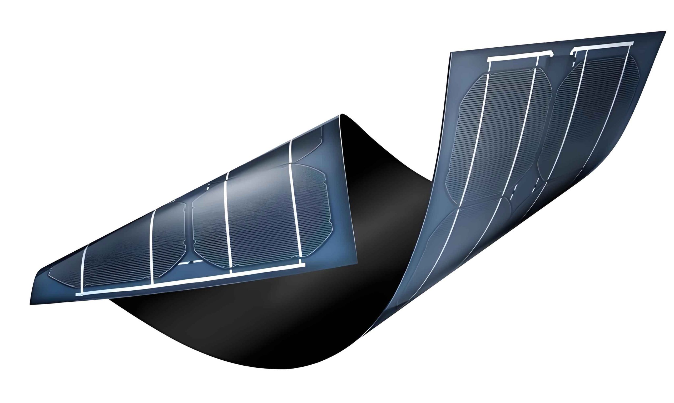
This pressing need for earth-abundant, non-toxic alternatives fueled intensive research into quaternary compounds like copper zinc tin sulfur/selenide (CZTSSe). As a kesterite-structured material composed of readily available elements, CZTSSe emerged as a champion for sustainable photovoltaics. Its bandgap is tunable (approximately 1.0-1.5 eV), and it possesses a high absorption coefficient (> 104 cm-1), making it theoretically suitable for high-performance thin film solar panels. The record efficiency for CZTSSe devices stands around 13%, a testament to its potential. Yet, progress has plateaued, largely due to the intrinsic complexity of this quinary system (Cu-Zn-Sn-S-Se). The thermodynamic stability region for the pure kesterite phase is narrow, leading to persistent issues with secondary phases (e.g., ZnS, Cu2SnS3) and a high concentration of detrimental point defects, such as CuZn antisites and SnZn defects. These defects act as recombination centers, severely limiting the open-circuit voltage (VOC)—a phenomenon known as the “VOC deficit.” The complex interplay of four cations makes precise stoichiometric and defect control during deposition and annealing extremely challenging, hindering further efficiency breakthroughs.
This context sets the stage for a paradigm shift: moving from complex multiinary compounds back to simpler, binary systems. The ideal candidate would combine elemental abundance, low toxicity, excellent optoelectronic properties, and straightforward synthetic control. It is within this search that germanium selenide (GeSe) has recently surged as a profoundly promising absorber material for the next generation of thin film solar panels.
Why Germanium Selenide (GeSe)? A Material-Centric Analysis
GeSe crystallizes in an orthorhombic structure (space group Pnma) and belongs to the group IV-VI semiconductors. Its appeal for photovoltaic applications can be quantitatively broken down into several key parameters, as summarized in the table below, comparing it with established and emerging thin film absorbers.
| Material | Bandgap (eV) | Absorption Coefficient α (cm-1) at E > Eg | Carrier Mobility μ (cm²/V·s) | Elemental Abundance & Toxicity | Theoretical S-Q Limit Efficiency (%)* |
|---|---|---|---|---|---|
| GeSe | ~1.14 | > 104 | ~128 (hole) | Abundant, Low-toxicity | >30 |
| CIGS | 1.0-1.7 (tunable) | > 105 | 10-100 | In, Ga scarce | ~33 |
| CdTe | ~1.45 | > 105 | ~10-100 | Cd toxic, Te scarce | ~32 |
| CZTSSe | ~1.0-1.5 | > 104 | ~1-10 | All abundant | ~33 |
| c-Si | ~1.12 | ~103 (indirect) | ~1500 (electron) | Abundant | ~33 |
* S-Q: Shockley-Queisser detailed-balance limit under AM1.5G spectrum.
1. Optimal Photovoltaic Bandgap: The Shockley-Queisser (S-Q) limit provides the theoretical maximum efficiency for a single-junction solar cell as a function of bandgap (Eg). The efficiency η is given by:
$$ \eta = \frac{J_{sc}V_{oc}FF}{P_{in}} $$
where Jsc is the short-circuit current density, Voc is the open-circuit voltage, and FF is the fill factor. Voc is fundamentally limited by the bandgap:
$$ V_{oc} \approx \frac{E_g}{q} – \frac{kT}{q} \ln\left(\frac{J_{00}}{J_{ph}}\right) $$
where J00 is the reverse saturation current density prefactor and Jph is the photocurrent density. The S-Q calculation shows a broad maximum for Eg between 1.1 eV and 1.4 eV. GeSe, with a direct bandgap of approximately 1.14 eV, sits perfectly within this optimal range, enabling efficient absorption of the solar spectrum while providing a high theoretical Voc potential.
2. Superior Optoelectronic Properties:
- High Absorption Coefficient (α): GeSe exhibits a direct bandgap transition with an absorption coefficient exceeding 104 cm-1 for photons with energy above its bandgap. This means that a film thickness of only about 1-2 μm is sufficient to absorb over 90% of the above-bandgap sunlight, fulfilling a primary requirement for cost-effective thin film solar panels. The absorption can be described by:
$$ \alpha(h\nu) = A(h\nu – E_g)^{1/2} $$
for a direct allowed transition, where A is a constant. - High Carrier Mobility (μ): Perhaps one of GeSe’s most distinguishing features is its exceptionally high hole mobility, reported to be around 128 cm²/V·s in high-quality crystals. High mobility reduces series resistance and improves carrier collection efficiency, especially in devices with less-than-perfect material quality. The conductivity σ is related to mobility and carrier concentration (p) by:
$$ \sigma = p e \mu_p $$
where e is the elementary charge. High μp allows for good conductivity even with moderate doping levels, reducing transport losses.
3. Material Simplicity and Stability: As a binary compound, GeSe sidesteps the phase stability quagmire of quaternary systems like CZTSSe. Its phase diagram is significantly simpler, reducing the probability of forming secondary phases during synthesis. Furthermore, GeSe exhibits remarkable ambient stability. Devices fabricated from GeSe have demonstrated negligible performance degradation over several months when stored in air without encapsulation, indicating a chemically stable and robust material—a critical practical advantage for thin film solar panels intended for long-term outdoor operation.
The Synthesis Challenge and the Innovative Rapid Thermal Sublimation (RTS) Solution
The potential of any material is only realized through the development of a scalable, high-quality fabrication process. For GeSe thin film solar panels, the primary synthesis challenge has been the control of phase purity. During conventional growth processes from the melt or via co-evaporation/sputtering, the formation of undesired phases like elemental germanium (Ge) or germanium diselenide (GeSe2) is thermodynamically competitive. These secondary phases act as recombination centers or create shunting paths, drastically degrading device performance.
A transformative solution to this problem emerged with the development of the Rapid Thermal Sublimation (RTS) technique. This method ingeniously leverages the unique sublimation characteristics of GeSe itself to achieve self-regulated, high-purity film growth. The core principles and advantages of RTS are as follows:
1. Self-Purification via Vapor Pressure Differential:
The RTS process involves placing a solid source of GeSe (which may initially contain impurities like Ge or GeSe2) in a closed or semi-closed chamber and rapidly heating it. The key lies in the significantly different saturation vapor pressures (Psat) of GeSe versus its common impurities. The vapor pressure of a solid follows the Clausius-Clapeyron relation:
$$ \ln P_{sat} = -\frac{\Delta H_{sub}}{RT} + C $$
where ΔHsub is the enthalpy of sublimation, R is the gas constant, T is the temperature, and C is a constant. The species with the highest vapor pressure at a given temperature will sublime preferentially. Experimental and theoretical data show that GeSe(s) sublimes at a substantially lower temperature and higher rate than Ge(s) or GeSe2(s). Therefore, during controlled RTS, the GeSe component selectively vaporizes, leaving behind most impurities in the source. The re-condensed film on the substrate is consequently of higher purity than the starting source material.
2. Defect Mitigation through Molecular Sublimation:
A profound insight into the sublimation mechanism reveals that GeSe sublimes not as monatomic Ge and Se vapors, but primarily as diatomic GeSe molecules:
$$ \text{GeSe}_{(s)} \rightarrow \text{GeSe}_{(g)} $$
This molecular sublimation pathway is crucial. If Ge and Se were to sublime independently, their recombination on the substrate would be stochastic, easily leading to point defects such as antisites (GeSe or SeGe) and vacancies (VGe, VSe). In contrast, the arrival of pre-bonded GeSe molecules onto the substrate surface promotes the direct incorporation of correct Ge-Se pairs into the growing crystal lattice. This “molecular delivery” mechanism intrinsically suppresses the formation of these detrimental point defects, leading to films with superior electronic quality and lower defect density (Nt), which is vital for achieving high VOC.
3. Unprecedented Growth Rate and Scalability:
Due to its high vapor pressure, GeSe can be sublimed and deposited at remarkably high rates. The RTS process has demonstrated deposition rates exceeding 4.8 μm/min. This is orders of magnitude faster than typical vacuum deposition techniques like thermal evaporation or sputtering. The implications for manufacturing thin film solar panels are substantial:
- Dramatically Reduced Energy Input: The process time per panel is minimized, lowering the thermal budget and overall energy consumption per watt produced.
- High Throughput: Fast deposition is a direct enabler for high-volume production, a critical economic factor for competing in the photovoltaic market.
- Simplified Process Control: The self-purifying nature reduces the need for extremely precise stoichiometric control of the source, simplifying the manufacturing workflow.
The successful application of RTS led to the fabrication of the first GeSe-based thin-film solar cell, which achieved a power conversion efficiency (PCE) of 1.48%. While this initial efficiency is modest, it represents a crucial proof-of-concept. More importantly, the device demonstrated a remarkably low VOC deficit in its early stage of development, suggesting that with optimized device architecture and interface engineering, there is a vast, relatively untapped potential for rapid efficiency gains.
Device Architecture, Loss Analysis, and Pathways to Higher Efficiency
The initial GeSe solar cells employed a simple substrate configuration: Glass/Mo/GeSe/CdS/i-ZnO/ITO. In this structure, molybdenum (Mo) serves as the back contact, GeSe is the p-type absorber, CdS is the n-type heterojunction partner forming the p-n junction, and the i-ZnO/ITO stack acts as the transparent conducting oxide (TCO) front contact. This structure immediately highlights areas for strategic improvement to push the efficiency of these thin film solar panels toward their theoretical limit.
| Loss Channel | Physical Origin | Quantitative Impact | Potential Mitigation Strategy |
|---|---|---|---|
| Low Short-Circuit Current (JSC) | Incomplete absorption; parasitic absorption in window layers (CdS); poor carrier collection. | Limits maximum photocurrent. Theoretical Jsc for Eg=1.14 eV is ~40 mA/cm². | Optimize GeSe thickness & texturing; replace CdS with wider-bandgap buffer (e.g., Zn(O,S), (Zn,Mg)O); improve minority carrier diffusion length Ln. |
| Low Open-Circuit Voltage (VOC) | Interface recombination at GeSe/buffer layer; bulk recombination via deep defects. | VOC deficit = (Eg/q) – VOC. The primary target for improvement. | Interface passivation (ALD Al2O3); post-deposition treatments (e.g., Sb doping, Se/Ge flux annealing); alternative heterojunction partners. |
| Low Fill Factor (FF) | High series resistance (Rs); low shunt resistance (Rsh); non-ideal diode behavior. | FF = (JmpVmp)/(JscVoc). Reduced by parasitic resistances. | Optimize TCO and back contact conductivity; reduce contact barriers; eliminate pinholes and secondary phases to increase Rsh. |
| Optical Losses | Reflection at air/TCO and TCO/buffer interfaces. | Can account for >5% absolute efficiency loss. | Implement anti-reflection coatings (MgF2, nanostructures); use light-trapping schemes. |
Key Strategies for Advancement:
1. Band Alignment Engineering: The conduction band offset (CBO) between GeSe and the buffer layer (e.g., CdS) is critical. A “spike”-type alignment (positive CBO) can block electron backflow but may also impede electron collection if too large. A “cliff”-type alignment (negative CBO) causes interface recombination. Using alternative buffers like Zn(O,S) allows tuning of the bandgap and electron affinity to achieve an optimal “flat” or small positive spike alignment, minimizing interface recombination velocity (S) and boosting VOC.
2. Defect Passivation and Doping Control: While RTS reduces defects, further post-deposition treatments can optimize the electrical properties. Controlled annealing in Se or Ge vapor can adjust the stoichiometry, reducing vacancy concentrations. Intentional doping, for instance with antimony (Sb) as an acceptor, could help achieve optimal carrier concentration (NA) for building a stronger depletion region:
$$ W = \sqrt{\frac{2\epsilon_r \epsilon_0 (V_{bi} – V)}{e N_A}} $$
where W is the depletion width, Vbi is the built-in potential, and V is the applied bias. An optimal NA ensures a wide enough W for carrier generation while maintaining a high Vbi.
3. Advanced Device Architectures: Moving beyond the simple substrate structure, superstrate configurations (where light enters through the glass substrate) could offer advantages. Furthermore, the exploration of hole transport layers (HTLs) at the back contact and electron transport layers (ETLs) at the front could evolve GeSe devices toward a more efficient p-i-n or graded structure, mimicking strategies from perovskite and organic photovoltaics.
Future Outlook and Broader Impact
The advent of high-quality GeSe thin films via techniques like RTS marks the opening of a new and exciting chapter in photovoltaic materials science. GeSe’s compelling combination of an ideal bandgap, high mobility, elemental abundance, and binary simplicity addresses the core limitations of both established (CdTe, CIGS) and emerging (CZTSSe) thin film technologies. Its demonstrated ambient stability further strengthens its case for practical application.
The initial efficiency of 1.48% is merely the starting point. The historical learning curves of other thin film technologies show that once a viable material system and fabrication method are identified, focused research on device physics and engineering can lead to exponential efficiency gains over a relatively short period. The primary focus for GeSe thin film solar panels will be on closing the VOC deficit through interface and bulk defect engineering. Given its high starting mobility and optimal bandgap, the pathway to efficiencies surpassing 15% and eventually approaching 20% is clearly delineated.
Beyond single-junction cells, the 1.14 eV bandgap of GeSe makes it an nearly ideal candidate for the bottom cell in a tandem configuration. A wide-bandgap top cell (e.g., perovskite with Eg ~ 1.7-1.8 eV) combined with a GeSe bottom cell could theoretically surpass the S-Q limit for single junctions, targeting efficiencies well above 30%. This potential for tandem applications significantly amplifies the long-term strategic importance of developing GeSe photovoltaic technology.
In conclusion, GeSe emerges not just as another experimental material, but as a fundamentally well-positioned contender with the inherent attributes needed for sustainable, high-performance, and scalable photovoltaics. Its development embodies the critical search for green, earth-abundant solutions in the renewable energy transition. As research intensifies on optimizing film quality, heterojunction interfaces, and device architectures, germanium selenide is poised to become a central focus in the quest to produce the next generation of efficient, reliable, and commercially viable thin film solar panels.