
In recent years, perovskite solar cells have emerged as a promising photovoltaic technology due to their excellent light absorption, tunable bandgaps, long carrier diffusion lengths, and low manufacturing costs. Among various configurations, p-i-n type wide-bandgap perovskite solar cells are particularly critical for developing perovskite/silicon tandem solar cells, which have the potential to exceed 35% efficiency. However, wide-bandgap perovskite films often suffer from high surface defect densities, leading to significant open-circuit voltage losses and reduced stability. In this study, we propose a novel interfacial passivation strategy using a mixture of 2-thiopheneethylamine iodide (TEAI) and methylamine iodide (MAI) to form a two-dimensional/three-dimensional (2D/3D) heterostructure on the perovskite surface. This approach effectively reduces defect states and improves charge transport, resulting in enhanced performance and stability of wide-bandgap perovskite solar cells.
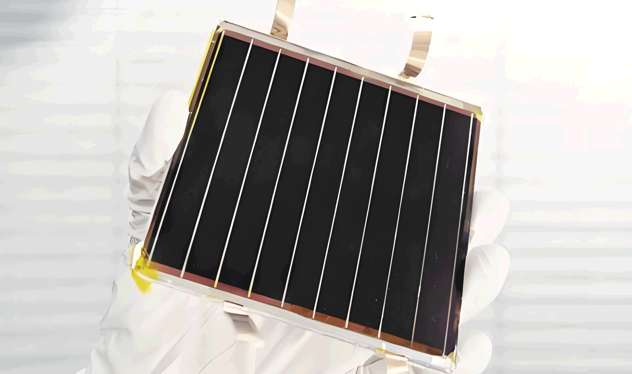
We fabricated perovskite solar cells with a structure of ITO/NiOx/perovskite/PC61BM/BCP/Au. The wide-bandgap perovskite layer, with a composition of FA0.78Cs0.22Pb(I0.85Br0.15)3 and a bandgap of 1.68 eV, was prepared by introducing additional CsCl and PbCl2. For passivation, we applied a solution containing TEAI and MAI in isopropanol onto the perovskite surface, followed by annealing. We compared three sample groups: control (unmodified), TEI (TEAI-only treated), and MTEI (TEAI and MAI co-treated). The surface morphology was characterized using atomic force microscopy (AFM), as shown in the following image:
The AFM results revealed that the TEI and MTEI treatments induced the formation of sheet-like structures, indicating the presence of a new perovskite phase. The root-mean-square (RMS) roughness decreased from 15.6 nm for the control to 10.3 nm for TEI and 9.39 nm for MTEI, suggesting smoother surfaces that facilitate better contact with charge transport layers. To investigate the crystallographic changes, we performed grazing-incidence X-ray diffraction (XRD). The control sample showed typical 3D perovskite peaks, while the TEI sample exhibited a new peak at 5.56°, corresponding to an n=1 2D perovskite phase. In contrast, the MTEI sample showed peaks at 4.03° and 8.23°, indicating an n=2 2D perovskite phase. This shift in n-value is attributed to the incorporation of MAI, which alters the A-site cation ratio and promotes the formation of higher-n 2D structures.
X-ray photoelectron spectroscopy (XPS) was used to analyze the chemical interactions. The Pb 4f peaks showed a significant shift for TEI and MTEI samples compared to the control, suggesting strong coordination between TEAI and uncoordinated Pb2+ ions, likely via sulfur atoms. This interaction passivates deep-level defects associated with Pb2+. Ultraviolet photoelectron spectroscopy (UPS) was employed to determine the energy level alignment. The calculated energy levels are summarized in Table 1, showing that the MTEI treatment resulted in a conduction band minimum (CBM) closer to that of the 3D perovskite, reducing energy level mismatch and minimizing interfacial recombination.
| Sample | Work Function (eV) | Valence Band Maximum (eV) | Conduction Band Minimum (eV) |
|---|---|---|---|
| Control | -3.95 | -5.19 | -3.51 |
| TEI | -4.38 | -5.50 | -3.14 |
| MTEI | -4.36 | -5.80 | -3.59 |
Steady-state photoluminescence (PL) and time-resolved photoluminescence (TRPL) measurements were conducted to study carrier dynamics. The PL intensity increased significantly for TEI and MTEI samples, indicating reduced non-radiative recombination. The TRPL decay curves were fitted using a bi-exponential function:
$$ y = A_1 \exp\left(-\frac{t}{\tau_1}\right) + A_2 \exp\left(-\frac{t}{\tau_2}\right) $$
where $\tau_1$ and $\tau_2$ represent fast and slow decay components, and $A_1$ and $A_2$ are their respective amplitudes. The average carrier lifetime $\tau_{\text{ave}}$ was calculated as:
$$ \tau_{\text{ave}} = \frac{A_1 \tau_1 + A_2 \tau_2}{A_1 + A_2} $$
The fitting parameters are listed in Table 2. The control sample had an average lifetime of 353.70 ns, which increased to 489.02 ns for TEI and 805.60 ns for MTEI, confirming effective passivation.
| Sample | $\tau_1$ (ns) | $\tau_2$ (ns) | $A_1$ (%) | $A_2$ (%) | $\tau_{\text{ave}}$ (ns) |
|---|---|---|---|---|---|
| Control | 8.35 | 353.83 | 1.54 | 98.46 | 353.70 |
| TEI | 35.91 | 490.06 | 3.02 | 96.98 | 489.02 |
| MTEI | 45.20 | 806.72 | 2.55 | 97.45 | 805.60 |
We evaluated the photovoltaic performance of the devices. The current density-voltage (J-V) curves under AM 1.5G illumination are shown in Figure 1b, and the key parameters are summarized in Table 3. The control device had an open-circuit voltage ($V_{\text{OC}}$) of 1.12 V, a short-circuit current density ($J_{\text{SC}}$) of 20.32 mA/cm², a fill factor (FF) of 78.77%, and a power conversion efficiency (PCE) of 17.99%. The TEI-treated device showed improved $V_{\text{OC}}$ (1.18 V) but reduced $J_{\text{SC}}$ (19.86 mA/cm²) and FF (77.79%), yielding a PCE of 18.08%. In contrast, the MTEI-treated device achieved a $V_{\text{OC}}$ of 1.20 V, $J_{\text{SC}}$ of 20.30 mA/cm², FF of 82.94%, and PCE of 20.19%. The hysteresis index (HI) was calculated as:
$$ \text{HI} = \frac{\text{PCE}_{\text{forward}} – \text{PCE}_{\text{reverse}}}{\text{PCE}_{\text{forward}}} \times 100\% $$
The HI values were 4.22% for control, 3.71% for TEI, and 2.53% for MTEI, indicating reduced hysteresis. External quantum efficiency (EQE) spectra confirmed the $J_{\text{SC}}$ values, with integrated currents of 19.01 mA/cm², 18.73 mA/cm², and 20.20 mA/cm² for control, TEI, and MTEI, respectively. Stability tests under maximum power point tracking showed that the MTEI device retained 96.68% of its initial PCE after 1000 s, compared to 94.45% for TEI and 83.14% for control.
| Sample | Scan Direction | $J_{\text{SC}}$ (mA/cm²) | $V_{\text{OC}}$ (V) | FF (%) | PCE (%) |
|---|---|---|---|---|---|
| Control | Forward | 20.32 | 1.12 | 78.77 | 17.99 |
| Reverse | 20.33 | 1.11 | 76.28 | 17.23 | |
| TEI | Forward | 19.86 | 1.18 | 76.79 | 18.08 |
| Reverse | 19.78 | 1.15 | 76.50 | 17.41 | |
| MTEI | Forward | 20.30 | 1.20 | 82.94 | 20.19 |
| Reverse | 20.31 | 1.18 | 82.13 | 19.68 |
To further understand the charge transport and recombination mechanisms, we performed electrochemical impedance spectroscopy (EIS). The Nyquist plots were fitted with an equivalent circuit model consisting of a series resistance ($R_s$), a recombination resistance ($R_{\text{rec}}$), and a constant phase element (CPE). The MTEI sample exhibited the highest $R_{\text{rec}}$, indicating suppressed non-radiative recombination. Space-charge-limited current (SCLC) measurements were used to quantify the trap density ($n_{\text{trap}}$) using the equation:
$$ n_{\text{trap}} = \frac{2 \varepsilon \varepsilon_0 V_{\text{TFL}}}{e L^2} $$
where $\varepsilon$ is the relative permittivity, $\varepsilon_0$ is the vacuum permittivity, $e$ is the elementary charge, $L$ is the perovskite thickness, and $V_{\text{TFL}}$ is the trap-fill limit voltage. The $V_{\text{TFL}}$ values were 0.256 V, 0.175 V, and 0.128 V for control, TEI, and MTEI, respectively, corresponding to trap densities of $4.32 \times 10^{15}$ cm⁻³, $2.95 \times 10^{15}$ cm⁻³, and $2.16 \times 10^{15}$ cm⁻³. This reduction in trap density is attributed to the coordination between TEAI and Pb2+ ions, which passivates surface defects. Dark J-V curves showed lower leakage currents for passivated devices, confirming reduced recombination. Mott-Schottky analysis revealed that the built-in potential ($V_{\text{bi}}$) increased from 1.02 V for control to 1.18 V for MTEI, enhancing the charge extraction efficiency.
In summary, we developed a synergistic passivation strategy using TEAI and MAI to form an n=2 2D/3D heterostructure on wide-bandgap perovskite films. This approach improved energy level alignment, reduced defect density, and enhanced charge transport, leading to a high-performance perovskite solar cell with a PCE of 20.19%, $V_{\text{OC}}$ of 1.20 V, and excellent operational stability. Our findings provide a effective pathway for advancing wide-bandgap perovskite solar cells in tandem applications.