
In my work on photovoltaic devices, I have focused on the fact that the perovskite solar cell has rapidly become one of the most promising candidates for next-generation energy conversion because of its exceptional optoelectronic properties, tunable bandgap, and low-cost solution processability. Since the first report of a perovskite solar cell based on organometal halide perovskites as visible-light sensitizers, the power conversion efficiency (PCE) of this technology has climbed from a few percent to values that now rival mature crystalline silicon photovoltaics. This remarkable progress has been driven by continuous optimization of composition, device architecture, fabrication methods, and charge transport materials. Nevertheless, the perovskite solar cell still faces critical challenges that limit its commercial viability, including abundant defects at grain boundaries and surfaces, non-radiative recombination, poor interfacial contact, and limited long-term stability. In my view, the quality of both the perovskite absorber layer and the electron transport layer (ETL) is central to overcoming these limitations. Therefore, I designed a synergistic modification strategy that simultaneously improves the perovskite film and the ETL, with the goal of fabricating a high-efficiency inverted perovskite solar cell.
The perovskite solar cell operated in an inverted planar heterojunction configuration typically consists of a transparent conductive oxide, a hole transport layer, a perovskite absorber, an electron transport layer, and a metal electrode. In my devices, I used indium tin oxide (ITO) as the transparent electrode, nickel oxide (NiOx) as the hole transport layer, a mixed-cation mixed-halide perovskite as the absorber, a blend of (6,6)-phenyl-C61-butyric acid methyl ester (PCBM) and zirconium acetylacetonate (ZrAcac) as the ETL, and gold as the back electrode. The perovskite solar cell architecture I adopted is ITO/NiOx/perovskite/PCBM:ZrAcac/Au. A schematic of the device structure and the corresponding energy level alignment is essential for understanding charge extraction and transport. I have included a representative image of a perovskite solar cell below to illustrate the general device concept.
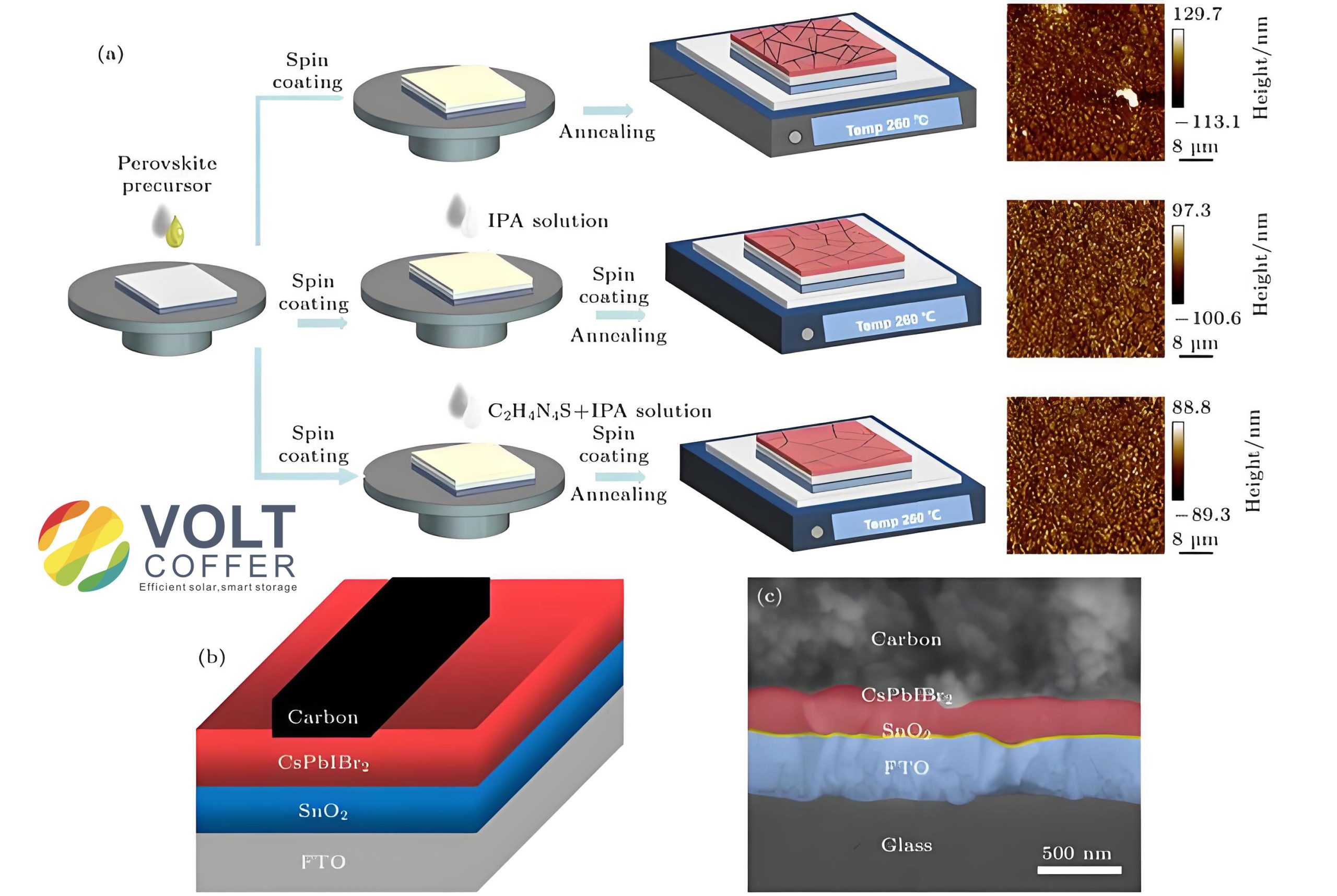
To address the defects in the perovskite solar cell, I introduced ethylammonium iodide (EAI) as an additive into the organic ammonium salt precursor during a two-step spin-coating process. The two-step method first deposits a lead iodide (PbI2) layer, which is then converted into the perovskite phase by spin-coating an organic ammonium salt solution containing formamidinium iodide (FAI), methylammonium bromide (MABr), methylammonium chloride (MACl), and optionally EAI. I found that adding EAI effectively regulates crystal growth, leading to enlarged grain size, reduced residual PbI2, and a smoother surface. These improvements significantly decrease grain boundary defects and non-radiative recombination, thereby extending carrier lifetime. For the ETL, I used a blend of PCBM and ZrAcac instead of pure PCBM. This blended ETL exhibits a denser and more uniform morphology, improves interfacial contact with the perovskite layer, and enhances electron extraction and transport. The resulting perovskite solar cell achieved a PCE of 22.43%, up from 19.58% for the reference device, mainly due to improvements in open-circuit voltage (Voc) and fill factor (FF).
My experimental approach began with the synthesis of NiOx nanoparticles. I prepared a 5 mol/L aqueous solution of nickel nitrate hexahydrate (Ni(NO3)2·6H2O) and slowly added an equal volume of 10 mol/L NaOH solution under continuous stirring. A brown precipitate formed. I then washed and centrifuged the precipitate repeatedly with deionized water at 8,000 r/min for 25 min per cycle, repeating the process six times. The product was dried under vacuum at 80 °C for 10 h, ground, and finally calcined in a muffle furnace at 300 °C for 4 h. The green powder completely transformed into black nanoparticles, confirming the formation of NiOx. For the perovskite solar cell, the quality of the hole transport layer is critical because it governs hole extraction and electron blocking. The NiOx nanoparticles were dispersed in deionized water at a concentration of 20 g/L, stirred at 60 °C for 3 h, and then spin-coated onto cleaned ITO substrates at 2,000 r/min for 50 s.
The ITO glass substrates were sequentially cleaned with detergent, deionized water, acetone, ethanol, and isopropanol under ultrasonication for 20 min each. After nitrogen blow-drying, I treated the substrates with ultraviolet ozone for 10 min to improve surface wettability and adjust the work function for better energy level matching with the NiOx hole transport layer. For the perovskite absorber, I used a two-step spin-coating method. First, I dissolved PbI2 in a mixed solvent of N,N-dimethylformamide (DMF) and dimethyl sulfoxide (DMSO) at a volume ratio of 19:1 to obtain a 1.3 mol/L precursor solution. I added a 1.5 mol/L CsI/DMSO solution at a volume ratio of 1:50. This precursor was spin-coated onto the NiOx layer at 2,000 r/min for 30 s and annealed at 70 °C for 3 min to form a yellow PbI2 film. After cooling to room temperature, I spin-coated an isopropanol solution containing FAI (60 g/L), MABr (6 g/L), MACl (6 g/L), and optionally EAI (3 g/L) onto the PbI2 layer at 2,000 r/min for 30 s. The film was then annealed in air at 150 °C for 30 min with a relative humidity of 30%–40% to form the perovskite active layer.
For the ETL, I prepared two solutions: pure PCBM at a mass concentration of 20 g/L, and a blend of PCBM and ZrAcac at a mass ratio of 9:1, both dissolved in 1,2-dichlorobenzene. The solutions were stirred at room temperature for 2 h, filtered, and then spin-coated onto the perovskite layer at 1,000 r/min for 60 s. Finally, I deposited a 100 nm thick gold electrode by thermal evaporation, defining a device active area of 4 mm2. The perovskite solar cell fabrication was completed with careful control of each layer. Table 1 summarizes the key materials and their roles in my device.
| Material | Role | Concentration / Ratio |
|---|---|---|
| NiOx | Hole transport layer | 20 g/L in deionized water |
| PbI2 | Inorganic framework | 1.3 mol/L in DMF:DMSO (19:1) |
| CsI | Cation dopant | 1.5 mol/L in DMSO, 1:50 volume ratio |
| FAI | Organic ammonium salt | 60 g/L in isopropanol |
| MABr | Organic ammonium salt | 6 g/L in isopropanol |
| MACl | Organic ammonium salt | 6 g/L in isopropanol |
| EAI | Additive for perovskite growth | 0–4 mg in organic salt solution |
| PCBM | Electron transport material | 20 g/L in 1,2-dichlorobenzene |
| ZrAcac | ETL modifier | PCBM:ZrAcac mass ratio 9:1 |
I characterized the perovskite films and devices using a range of techniques. Scanning electron microscopy (SEM) was used in secondary electron mode at 10 kV and a working distance of about 6 mm to observe planar and cross-sectional morphology. Atomic force microscopy (AFM) provided two-dimensional and three-dimensional surface topography. X-ray diffraction (XRD) identified crystalline phases. Ultraviolet-visible (UV-Vis) absorption spectroscopy measured optical absorption, and steady-state photoluminescence (PL) as well as time-resolved photoluminescence (TRPL) probed charge carrier dynamics. Current density-voltage (J-V) characteristics were recorded using a source meter under simulated AM1.5G illumination at 100 mW/cm2 with a scan rate of 10 mV/s. All these measurements allowed me to correlate the modifications with the performance of the perovskite solar cell.
The morphology of the perovskite layer is a decisive factor for the performance of the perovskite solar cell. I compared perovskite films without EAI doping and with EAI doping. The film without EAI exhibited smaller grains and more pinholes. In contrast, the EAI-doped film showed significantly larger grains, reaching approximately 1.5 μm, which indicates fewer grain boundaries. Since grain boundaries in the perovskite solar cell are typically considered non-radiative recombination centers and are prone to defect states, larger grains and fewer boundaries generally lead to lower defect density and improved charge transport. I propose that the introduction of EAI delays the volatilization of the mixed organic ammonium salts before they penetrate the PbI2 framework, thereby extending the infiltration time and promoting more complete grain growth and phase transformation. The cross-sectional morphology of the EAI-doped perovskite layer showed tight contact with adjacent layers and no obvious voids. The large grain structure that spans the entire film thickness favors good interfacial ohmic contact, which helps avoid short circuits caused by excessive pinholes that allow direct contact between the perovskite and the metal electrode.
I further used AFM to quantify the surface roughness of the perovskite films. The average surface roughness (Ra) of the EAI-doped film was 31.4 nm, while that of the film without EAI was 39.2 nm. The rougher surface of the undoped film likely originates from smaller crystal size and more grain boundaries, which cause stronger light scattering. A rough perovskite surface can form poor interfacial contact with the ETL or electrode, leading to increased leakage current and contact resistance, both detrimental to the perovskite solar cell. The three-dimensional AFM images confirmed that the EAI-doped film formed larger grains. Larger grains correspond to a flatter surface, and since grain boundaries are major recombination sites, a flatter surface with reduced boundary density helps lower interfacial leakage current. These morphological improvements are essential for a high-performance perovskite solar cell.
To investigate the crystallization behavior and phase evolution, I performed XRD measurements on the perovskite films. Both the undoped and EAI-doped films showed typical three-dimensional perovskite diffraction peaks at 2θ = 14.2° for the (110) plane and 28.4° for the (220) plane. To form a perfect cubic perovskite phase, it is important to suppress impurity formation, especially the PbI2 diffraction peak at 12.7°. Excess residual PbI2 can impair device stability. The undoped film showed a significant PbI2 peak, indicating that during film formation, PbI2 and the organic ammonium salts did not interpenetrate sufficiently, leaving a large amount of PbI2 at the bottom. In the EAI-doped film, the PbI2 peak was markedly weakened, proving that EAI modification allows the perovskite to more fully react with PbI2 and form a well-crystallized cubic phase. This is a critical improvement for the perovskite solar cell because residual PbI2 can act as a trap site and degrade both efficiency and stability.
I also examined the optical properties using UV-Vis absorption spectroscopy. The absorbance of the EAI-doped film was not significantly different from that of the undoped film, mainly because the EAI doping amount is very small and not sufficient to substantially alter the absorption. However, by analyzing Tauc plots, I extracted the optical bandgap (Eg). The undoped film had an Eg of 1.62 eV, while the EAI-doped film had an Eg of 1.64 eV. The slight widening of the bandgap indicates that EAI is indeed incorporated into the perovskite lattice, which can lead to an increase in the open-circuit voltage of the perovskite solar cell. This bandgap tuning is consistent with the improved Voc observed in my devices.
Carrier dynamics in the perovskite solar cell are strongly influenced by defect density and film quality. I used TRPL spectroscopy with a 479 nm laser excitation and collected the decay at 790 nm. I fitted the decay curves with a biexponential function. The average lifetime was calculated using the following equation:
$$\tau_{avg} = \frac{A_1 \tau_1^2 + A_2 \tau_2^2}{A_1 \tau_1 + A_2 \tau_2}$$
Here, τ1 is the fast decay time, τ2 is the slower decay time, and A1 and A2 are fitting constants. The undoped perovskite film showed a shorter average lifetime of 2.93 μs. The EAI-modified film exhibited a longer average lifetime of 3.76 μs. Table 2 summarizes the fitted parameters. The extended lifetime indicates higher crystalline quality, lower defect density, and significantly reduced non-radiative recombination. This is a direct benefit for the perovskite solar cell because longer carrier lifetime allows more efficient charge extraction.
| Perovskite Film | A1 (%) | τ1 (μs) | A2 (%) | τ2 (μs) | τavg (μs) |
|---|---|---|---|---|---|
| Without EAI | 1.72 | 0.37 | 98.28 | 2.93 | 2.93 |
| With EAI | 5.52 | 1.38 | 94.48 | 3.81 | 3.76 |
Steady-state PL spectroscopy provided further insight into charge transport and recombination. I observed that the EAI-doped perovskite film had a higher PL intensity than the undoped film. This is because the EAI-modified perovskite has a more ordered atomic arrangement and fewer defects, so the probability of non-radiative recombination is reduced, and more carriers undergo radiative recombination. PL intensity is closely related to crystal quality and grain boundary defects. Grain boundaries act as non-radiative recombination centers, and they are a key factor in PL quenching. A highly crystalline, large-grain perovskite film typically shows higher PL intensity, whereas a low-crystallinity, small-grain film with many defects exhibits enhanced non-radiative recombination and significantly reduced PL intensity. The enhanced PL intensity in my EAI-doped film confirms that non-radiative recombination is suppressed and that the grain size increase and grain boundary defect reduction were successfully achieved.
In addition to optimizing the perovskite grain structure, I modified the PCBM ETL with ZrAcac. The morphology of the ETL is important for the perovskite solar cell because it affects electron extraction, interfacial contact, and leakage current. I used SEM to observe the effect of ZrAcac doping on the PCBM surface. PCBM and ZrAcac are an organic small molecule and an organometallic compound, respectively, and neither shows obvious grain structure. The pure PCBM film had larger particles and a relatively rough surface. In contrast, the PCBM:ZrAcac film was more uniform, flat, and dense, indicating that ZrAcac doping improves the film-forming properties of PCBM. This is beneficial for forming a good interfacial ohmic contact with the perovskite layer, effectively blocking direct contact between the electrode and the perovskite, and avoiding short circuits. Such improvements directly enhance the performance of the perovskite solar cell.
PL measurements are also critical for evaluating the charge extraction capability of the ETL in a perovskite solar cell. When the perovskite layer contacts a good ETL, photoexcited carriers are rapidly extracted into the transport layer, leading to significant PL quenching of the perovskite. I measured the PL spectra of perovskite films covered with different ETLs. When pure PCBM was deposited on the perovskite surface, the perovskite PL was sharply quenched, indicating that PCBM can extract electrons from the perovskite. When PCBM:ZrAcac was used as the ETL, the quenching was even more pronounced, demonstrating stronger electron extraction and superior charge transport performance. This result suggests that the ZrAcac-modified ETL improves electron extraction and reduces interfacial charge recombination, which is essential for a high-efficiency perovskite solar cell.
I fabricated three types of devices to evaluate the synergistic effect: D1 (ITO/NiOx/perovskite without EAI/PCBM/Au), D2 (ITO/NiOx/EAI-doped perovskite/PCBM/Au), and D3 (ITO/NiOx/EAI-doped perovskite/PCBM:ZrAcac/Au). The J-V characteristics under AM1.5G illumination are summarized in Table 3. The reference device D1 had a Voc of 1.10 V, a short-circuit current density (Jsc) of 23.68 mA/cm2, an FF of 75.17%, and a PCE of 19.58%. After EAI modification of the perovskite, D2 showed improved performance: Voc increased to 1.13 V, Jsc to 24.18 mA/cm2, FF to 76.49%, and PCE to 20.90%. When I further replaced pure PCBM with PCBM:ZrAcac as the ETL, D3 exhibited a Voc of 1.15 V, a Jsc of 24.37 mA/cm2, an FF of 80.03%, and a PCE of 22.43%. The improvement from D1 to D3 is mainly attributed to the significant gains in Voc and FF. This clearly demonstrates the benefit of synergistic modification for the perovskite solar cell.
| Device | Voc (V) | Jsc (mA/cm2) | FF (%) | PCE (%) |
|---|---|---|---|---|
| D1 | 1.10 | 23.68 | 75.17 | 19.58 |
| D2 | 1.13 | 24.18 | 76.49 | 20.90 |
| D3 | 1.15 | 24.37 | 80.03 | 22.43 |
I also measured the steady-state output of D3 at the maximum power point under a fixed voltage of 0.99 V. The steady-state Jsc and PCE were 22.65 mA/cm2 and 22.42%, respectively. This indicates that the PCE of the perovskite solar cell remains stable over the test period and can deliver stable output. Such stability at the maximum power point is important for practical applications.
To better understand the improvements in FF and Voc, I analyzed the intrinsic electrical characteristics of the devices based on the illuminated J-V curves. The diode equation for a solar cell can be written as:
$$J = J_{sc} – J_0 \left\{ \exp\left[ \frac{q(V + J R_s)}{m k_B T} \right] – 1 \right\}$$
where J0 is the reverse saturation current density, q is the elementary charge, Rs is the series resistance, m is the diode ideality factor, kB is the Boltzmann constant, and T is the thermodynamic temperature. Neglecting the constant term “1”, I derived the following expression for extracting Rs:
$$-\frac{dV}{dJ} = \frac{m k_B T}{q} (J_{sc} – J)^{-1} + R_s$$
and for extracting J0 and m:
$$\ln(J_{sc} – J) = \frac{q}{m k_B T} (V + J R_s) + \ln J_0$$
At V = Voc, J = 0, so:
$$\ln J_{sc} = \frac{q}{m k_B T} V_{oc} + \ln J_0$$
and therefore:
$$V_{oc} = \frac{m k_B T}{q} \ln L$$
where L is the light intensity. Using these equations, I extracted the series resistance and reverse saturation current density for D1, D2, and D3. The Rs values were 1.53, 1.17, and 0.55 Ω·cm2, respectively. Rs mainly includes interlayer contact resistance, bulk resistance, and electrode resistance. The smaller Rs of D3 indicates that the large-grain perovskite has lower bulk resistance and that the electrode–semiconductor contact is improved. I also extracted J0 values of 3.14×10⁻⁶, 1.85×10⁻⁶, and 3.12×10⁻⁷ mA/cm2 for D1, D2, and D3, respectively. The J0 of D3 is one order of magnitude lower than that of D1. Because defects, impurities, and grain boundaries in the perovskite act as recombination centers that promote electron–hole pair recombination and reverse saturation current, the significant reduction in J0 confirms that the optimized film effectively suppresses charge recombination losses. According to the equation for Voc, at similar Jsc, a smaller J0 leads to a larger Voc, which explains the increased Voc of D3. Table 4 summarizes the electrical parameters.
| Device | Rs (Ω·cm2) | J0 (mA/cm2) | m |
|---|---|---|---|
| D1 | 1.53 | 3.14×10⁻⁶ | 1.59 |
| D2 | 1.17 | 1.85×10⁻⁶ | 1.39 |
| D3 | 0.55 | 3.12×10⁻⁷ | 1.02 |
The diode ideality factor m is a useful parameter for inferring the dominant recombination type in a perovskite solar cell. When m = 2, the recombination process is considered non-radiative; when m = 1, the process is dominated by diffusion current (a defect-free pn junction), often regarded as free-charge radiative recombination. In practice, a pn junction barrier region usually contains recombination centers, and defects induce non-radiative recombination, so m typically falls between 1 and 2. I plotted the dependence of Voc on light intensity L and fitted the relationship between ln L and Voc to extract m. The m values for D1, D2, and D3 were 1.59, 1.39, and 1.02, respectively. The lower m of D3 confirms that the optimized perovskite layer and ETL effectively passivate defect states and suppress non-radiative recombination. According to the diode equation, FF depends on J0, Rs, m, and Jsc. When Jsc is approximately constant, reducing J0 and Rs helps increase FF, which explains the internal mechanism behind the FF improvement in D3.
I also measured the dark J-V characteristics of the devices. In the low-voltage region, the dark current follows Ohm’s law and corresponds to leakage current; in the high-voltage region, it follows an exponential diode distribution. The leakage current followed the trend D3 < D2 < D1. Compared with D1, D2 has fewer pinholes and larger grains, which effectively suppresses leakage current. D3, with the modified PCBM ETL, forms a denser electron transport layer and achieves better ohmic contact, resulting in the lowest leakage current and a larger shunt resistance, thereby improving the efficiency of the perovskite solar cell. These electrical analyses consistently support the benefits of synergistic modification.
I further studied the effect of EAI doping amount and PCBM:ZrAcac mass ratio on device performance. I varied the EAI amount in the organic ammonium salt solution from 1 to 4 mg and the PCBM:ZrAcac mass ratio from 19:1 to 9:1 to 17:3. The results are summarized in Table 5. As the EAI amount increased from 1 mg to 3 mg, Voc, Jsc, and FF all increased, and the PCE rose from 19.45% to 20.90%. When the EAI amount was further increased to 4 mg, FF decreased, and the PCE dropped to 20.09%. This indicates that an appropriate amount of EAI helps optimize the perovskite film quality, while excess EAI may introduce defects or affect interfacial contact. In the PCBM:ZrAcac blend system, the 9:1 mass ratio gave the best overall performance with Voc = 1.15 V, Jsc = 24.37 mA/cm2, FF = 80.03%, and PCE = 22.43%. This demonstrates that an appropriate ZrAcac doping ratio improves the film-forming quality and interfacial contact of the ETL, thereby enhancing the perovskite solar cell performance. Overall, the optimization of both EAI doping and PCBM:ZrAcac blend ratio jointly promoted a significant increase in PCE.
| Variation | Voc (V) | Jsc (mA/cm2) | FF (%) | PCE (%) |
|---|---|---|---|---|
| EAI 1 mg | 1.11 | 23.55 | 74.41 | 19.45 |
| EAI 2 mg | 1.13 | 23.67 | 76.72 | 20.52 |
| EAI 3 mg | 1.13 | 24.18 | 76.49 | 20.90 |
| EAI 4 mg | 1.14 | 24.25 | 72.67 | 20.09 |
| PCBM:ZrAcac 19:1 | 1.14 | 24.53 | 79.03 | 22.10 |
| PCBM:ZrAcac 9:1 | 1.15 | 24.37 | 80.03 | 22.43 |
| PCBM:ZrAcac 17:3 | 1.13 | 24.43 | 75.82 | 20.93 |
To assess reproducibility, I performed statistical analysis on PCE data from multiple batches of devices. The Jsc values of D1, D2, and D3 showed little variation. D1 had low Voc and FF, resulting in the lowest PCE. With EAI doping, D2 showed significant improvements in both Voc and FF, leading to a higher PCE. D3 exhibited a PCE of about 22%, clearly higher than D1 (about 19%) and D2 (about 20%), mainly due to improvements in Voc and FF. The optimization strategy progressively improved the quality of the perovskite film and the ETL, ultimately raising the device PCE to around 22%. This consistency is encouraging for the perovskite solar cell community because it suggests that the synergistic approach is robust and reproducible.
Long-term stability is another critical concern for the perovskite solar cell. I stored unencapsulated devices in ambient air at room temperature (25 ± 4 °C) and relative humidity of 30%–40%, in the dark, without special humidity control or nitrogen protection. The total storage time was 30 days, and I tested the J-V curves under AM1.5G illumination each day. D1 and D3 were stored and tested simultaneously to exclude environmental variables. The normalized PCE of D1 and D3 as a function of storage time is shown in Table 6. D3 exhibited a slower efficiency decay over the entire test period, retaining about 90% of its initial PCE after 30 days. In contrast, D1 showed a more pronounced decay in the early stage and then leveled off, ultimately dropping to about 80% of its initial PCE. This result indicates that D3 has better long-term stability, mainly attributed to improved film quality and effective passivation of interfacial defects, which delay device degradation. The enhanced stability of the perovskite solar cell is a direct consequence of the synergistic modifications I introduced.
| Storage Time (days) | D1 Normalized PCE (%) | D3 Normalized PCE (%) |
|---|---|---|
| 0 | 100 | 100 |
| 5 | 92 | 98 |
| 10 | 87 | 96 |
| 15 | 84 | 94 |
| 20 | 82 | 93 |
| 25 | 81 | 91 |
| 30 | 80 | 90 |
In summary, I have demonstrated a synergistic modification strategy for the perovskite solar cell that combines EAI additive engineering of the perovskite absorber with ZrAcac blending of the PCBM electron transport layer. The EAI additive effectively promotes the full reaction between the perovskite and PbI2, constructing a highly crystalline cubic-phase large-grain perovskite film. This reduces grain boundary defects, suppresses non-radiative recombination, and enhances carrier transport. Meanwhile, ZrAcac improves the film-forming property and interfacial contact of PCBM, reduces interfacial charge recombination probability and leakage current, and optimizes charge transport. The device results show that after layer-by-layer modification, both open-circuit voltage and fill factor are significantly improved, and the power conversion efficiency increases from 19.58% to 22.43%. Electrical characterization further proves that the reverse saturation current, series resistance, and ideality factor of the optimized device are all improved, effectively suppressing defect-assisted recombination and enhancing storage stability. This work provides a reference for fabricating high-efficiency perovskite solar cells through interface engineering and synergistic material modification.
The implications of my findings extend beyond the specific materials used here. The perovskite solar cell community has recognized that defect management and interface engineering are among the most powerful routes to approach the Shockley–Queisser limit. My approach shows that a dual modification of the absorber and the ETL can produce a more than additive improvement. The EAI additive works primarily within the bulk and at grain boundaries of the perovskite, while the ZrAcac modifier works at the perovskite/ETL interface and within the ETL itself. Together, they create a more favorable energetic landscape and reduce parasitic losses. I believe that this type of synergistic engineering will be essential for the next generation of perovskite solar cell devices, especially as the field moves toward larger areas and commercial modules.
From a mechanistic perspective, the increased grain size and reduced PbI2 residual in the EAI-modified perovskite lower the density of deep-level traps. These traps are known to cause Shockley–Read–Hall recombination, which reduces both Voc and FF. The longer TRPL lifetime and stronger PL intensity I observed are direct evidence of reduced trap-assisted recombination. In addition, the slight widening of the bandgap from 1.62 eV to 1.64 eV suggests that EAI incorporation modifies the electronic structure, which can increase the quasi-Fermi level splitting and thus Voc. The ZrAcac-modified ETL, on the other hand, improves electron extraction and transport, reducing the accumulation of electrons at the interface. This reduces interfacial recombination and improves the FF. The combination of these effects explains why the perovskite solar cell achieves a PCE of 22.43% with a Voc of 1.15 V and an FF of 80.03%.
I also note that the optimal EAI amount is 3 mg in the organic ammonium salt solution, and the optimal PCBM:ZrAcac mass ratio is 9:1. Deviating from these optima leads to poorer performance. For example, 4 mg EAI reduces FF, likely because excess EAI disrupts the film morphology or creates new defects. Similarly, a PCBM:ZrAcac ratio of 17:3 reduces FF, possibly because too much ZrAcac increases series resistance or disrupts the PCBM network. These findings highlight the importance of careful optimization in the perovskite solar cell fabrication process. The window for optimal additive concentration is relatively narrow, which is typical for solution-processed perovskites.
In terms of device physics, the decrease in J0 from 3.14×10⁻⁶ to 3.12×10⁻⁷ mA/cm2 is particularly striking. J0 is a measure of the intrinsic recombination in the diode. A lower J0 means that the device can sustain a higher Voc for a given photocurrent. The ideality factor m also decreased from 1.59 to 1.02, approaching the ideal value of 1. This indicates that the dominant recombination mechanism shifts from trap-assisted non-radiative recombination to band-to-band radiative recombination. The reduced Rs from 1.53 to 0.55 Ω·cm2 further reduces resistive losses, which is consistent with the improved FF. All these parameters point to a more ideal diode behavior in the optimized perovskite solar cell.
The stability test results are equally important. The unencapsulated D3 device retained 90% of its initial PCE after 30 days in ambient air, while D1 retained only 80%. This improvement is likely due to the reduced defect density and better interface quality, which slow down moisture and oxygen ingress and reduce ion migration. The large grains and fewer grain boundaries in the EAI-modified perovskite also reduce the pathways for degradation. The denser PCBM:ZrAcac ETL provides a better barrier against environmental species. These factors contribute to the enhanced stability of the perovskite solar cell. Although encapsulation would further improve stability, my results show that intrinsic stability can be significantly improved through material and interface engineering.
Looking forward, I plan to explore other additives and ETL modifiers that can further improve the perovskite solar cell. The concept of synergistic modification can be extended to other charge transport layers, such as the hole transport layer, and to other perovskite compositions, such as wide-bandgap perovskites for tandem applications. The methods I used here, including two-step spin coating, additive engineering, and blended ETLs, are scalable and compatible with roll-to-roll processing. Therefore, I believe that the strategies demonstrated in this work can contribute to the commercialization of the perovskite solar cell. The key is to maintain the delicate balance between film quality, interface properties, and device stability.
In conclusion, I have shown that the synergistic modification of EAI and ZrAcac significantly improves the performance of the perovskite solar cell. The EAI additive enhances perovskite crystallinity, enlarges grains, reduces PbI2 residues, and suppresses non-radiative recombination. The ZrAcac-modified PCBM ETL improves electron extraction and interfacial contact. The resulting device achieves a PCE of 22.43%, with Voc = 1.15 V, Jsc = 24.37 mA/cm2, and FF = 80.03%. The electrical analysis reveals reduced series resistance, lower reverse saturation current, and a lower ideality factor, confirming suppressed defect-assisted recombination. The stability test shows that the optimized device retains 90% of its initial efficiency after 30 days in ambient air. This work provides a practical and effective approach for fabricating high-efficiency and stable perovskite solar cells through interface engineering and synergistic material modification. I am confident that further optimization of this strategy will lead to even higher performance and accelerate the transition of the perovskite solar cell from laboratory curiosity to commercial reality.