
The core control chip of this solar micro-inverter is TI’s TMS320F28035 chip. The software functions of this solar inverter mainly include maximum power point tracking, phase-locked loop, digital power conversion algorithm, and state machine.
1. State machine
The state machine is used to determine the operating mode of the solar inverter system. The interrupt service routine is executed once every 100us within the timer.There are three system states: system error, system start, and day mode.
When powered on, the system status is initialized to: system error.
When the ON/OFF switch is turned off, or any of the following faults occur, the state machine will switch to the system error mode:
(1) PV undervoltage/overvoltage;
(2) Grid undervoltage/overvoltage;
(3) Grid under-frequency/over-frequency;
(4) Drive power supply under/overvoltage;
(5) flyback MOSFET overcurrent;
(6) Flyback output overvoltage;
(7) 2.5V reference undervoltage/overvoltage;
(8) AC current detection offset;
(9) Solar inverter output overcurrent;
(10) Hardware zero crossing;
(11) The system is overheated.
When the ON/OFF switch is turned on and the system does not detect a fault within 500ms, the state machine will switch to the system start state.At this point, when the total number of zero crossing events exceeds 60, the system state machine switches to the day mode.
Day mode is the normal working mode of solar micro-inverters.Load sharing and maximum power point are both invoked in this mode.During this period, if the ON/OFF switch is switched to the OFF position or fails, the system will switch to the system error mode.
2. Device peripheral configuration
The TMS320F28035 provides the following intelligent peripherals: a high-speed analog comparator module, a high-speed PWM module, and a high-speed 10-bit ADC module for controlling comparator fault handling, high-resolution PWM, and flexible ADC triggering.
Three analog comparator modules are used to protect the inverter system: one for flyback output overvoltage protection, and two for flyback overcurrent protection.For overvoltage protection ISR, all PWM channels are placed in a rewrite state, followed by setting a critical fault flag.When the system is operating in day mode, the reference voltage is updated in the system state machine.
The system uses three PWM generators: one drives the full-bridge de-bounce circuit, and the other two drive the interleaved active clamp flyback converters.The PWM configuration of the full-bridge de-bounce circuit is to switch at four times the flyback converter frequency (228KHZ).One PWM channel performs switching operations during half a cycle, and the other half is placed in a rewrite state.The active clamp flyback PWM generator is configured with a dead zone time of 50ns and a standby dead zone time of 250ns.When an overcurrent condition occurs, the analog comparator will trigger the PWM module to turn off. To prevent accidental turn-off caused by noise generated by the switching of field-effect transistors, leading edge blanking (LEB) has been enabled, with a configuration time of 240ns.
PWM1 and PWM2 trigger the ADCs at precise times, allowing them to sample and convert the four ADC pairs.PWM1 triggers ADC pair 0, and PWM2 triggers the other three: ADC pairs 1, 3, and 5. ADC pair 0 has the highest priority.The ADC interrupt (ADCP3) is used to read the ADC result buffer. When this interrupt occurs, pairs 0, 1, and 3 are available, while pair 5 is still in the sampling and conversion process.
3. Maximum power point tracking (MPPT) algorithm and its programming
3.1 Maximum Power Point Tracking (MPPT) Algorithm
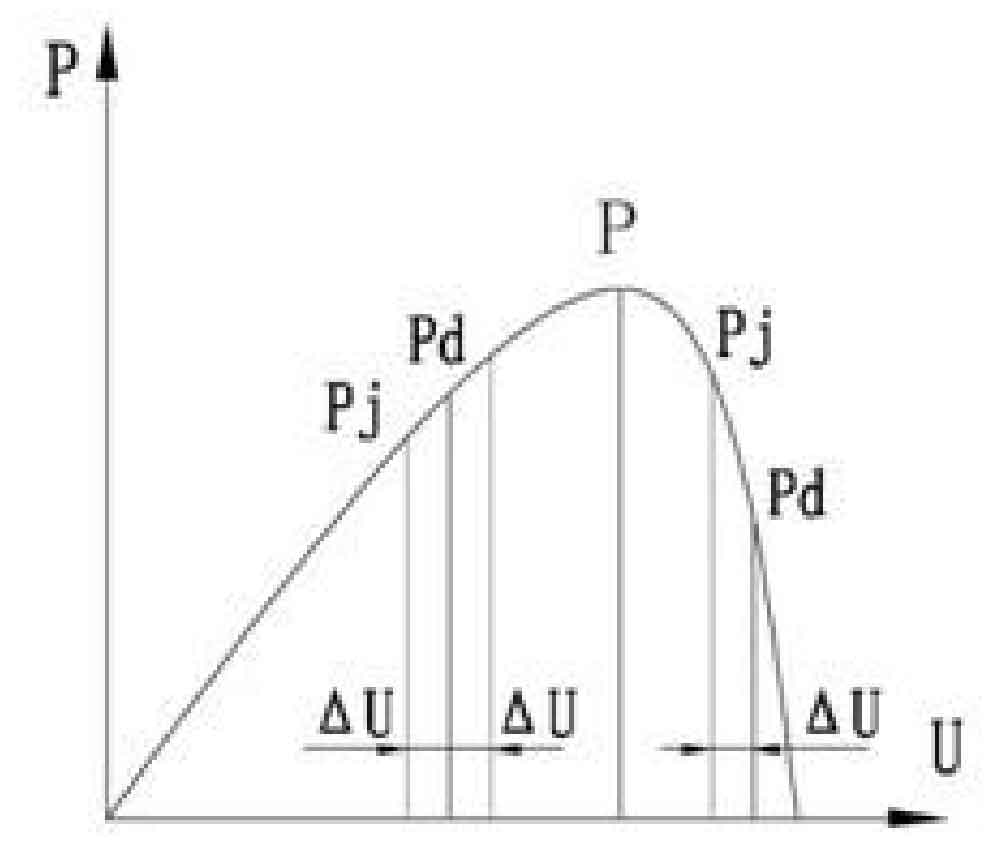
There are two commonly used methods to achieve MPPT: perturbation observation method and incremental conductance method.Both methods actually use ΔP instead of dp, resulting in dp/du=0, which means the reciprocal of power to voltage is zero.The only difference between the two methods is that the perturbation observation method uses ΔP=P(k)-P(k-1), which approximates dp by the difference between the power of the previous and current time.The curve composed of voltage and power is a parabola, as shown in Figure 1. When the voltage increases, if ΔP>0, it indicates that point k is on the left side of the maximum power point, and the voltage should be increased.Similarly, if ΔP<0 when increasing the voltage, it indicates that point k is on the right side of the maximum power point, and the voltage should be decreased.Ultimately, it will be at the maximum power point.
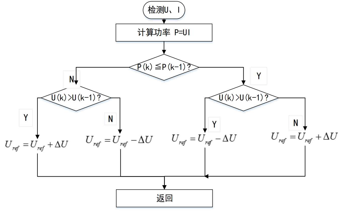
The flowchart of the fixed step disturbance observation method is shown in Figure 2.
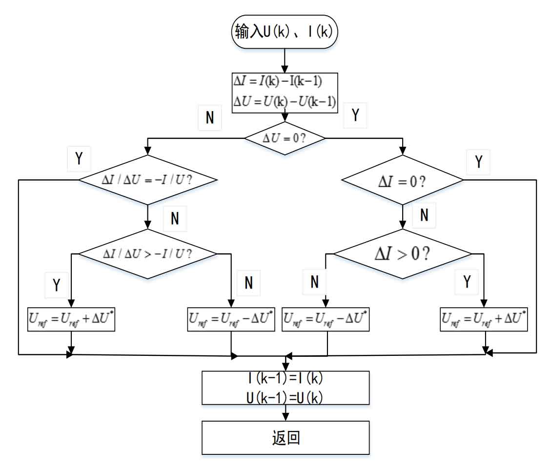
The so-called conductance increment method is to approximate dP with the total differential ΔP=U*ΔI+I*ΔU.The instantaneous output power of the photovoltaic cell is P=I*U.Derivating both sides with respect to U, we obtain: dP/dU = I + U dI/dU.When dP/dU=0, the output power of the photovoltaic cell reaches its maximum, at which point: dI/dU = -I/U.In practical calculations, dI/dU is often approximated by ΔI/ΔU, based on the following criteria:
When ΔP/ΔU>0, it means that the reciprocal of power to voltage is greater than zero, and point k is on the left of the maximum power point at the current power point;
When ΔP/ΔU=0, it means that the reciprocal of power to voltage is equal to zero, and point k is at the maximum power point at the current power point;
When ΔP/ΔU<0, it means that the reciprocal of power to voltage is less than zero, and point k is on the right side of the maximum power point at the current power point;
The flowchart of the conductance incremental method is shown in Figure 3.
3.2 Programming related to maximum power point tracking (MPPT)
The DSP integrated development environment CCS (Code Composer Studio) from TI is used for programming. This software integrates code writing, compiling, debugging, FLASH programming, and other functions, and is widely used due to its real-time and high-efficiency characteristics.
The main program mainly performs the following functions: measuring the working state, determining the start and stop, initializing and monitoring the system, and waiting for interruptions.Among them, the initialization of the system refers to the initialization of general purpose registers, event management modules, and special function registers.
The DC-DC and DC-AC links of the photovoltaic inverter are both controlled using closed-loop control, with a pulse width modulation (PWM) conversion frequency of 50KHZ for the interrupt service program to control the DC flyback and AC inverter, and 1KHZ for the interrupt service subroutine to drive the state machine, maximum power point tracking, and power measurement functions.
The program for MPPT in the DC-DC stage consists of the following four parts:
(1) Main program part: mainly completes application initialization, peripheral configuration, application management, slower background program loop, and task timing arrangement;
(2) The initialization of external devices such as clocks, phase-locked loops, and general-purpose IO interfaces, as well as enabling the clock for external devices;
(3) Setting of global variables
(4) Nested part of the program
4. Solar inverter output current and grid voltage in phase method
This solar inverter mainly achieves two functions: obtaining electrical energy from solar panels and making the output current of the solar inverter in phase with the grid voltage.Among them, the maximum power point tracking (MPPT) technology involved in obtaining electrical energy from solar panels has been described in detail earlier.Next, we will detail how to study the in-phase relationship between the output current of the solar inverter and the grid voltage.
The known expression for the grid voltage is: U=U0Sin(ωt+ψ)
To make the solar inverter output current in phase with the grid voltage, simply make: I=I0Sin(ωt+ψ)
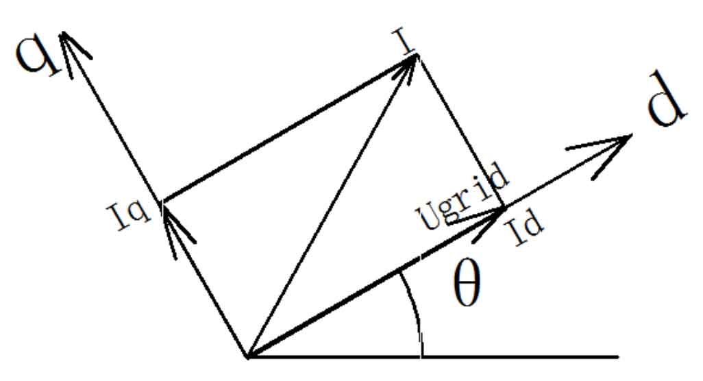
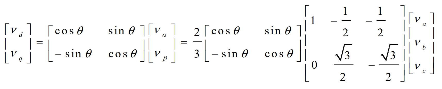
First, a phase-locked loop is used to make the phase angle of the solar inverter output current equal to the phase angle of the grid voltage ωt (θ in Figure 4), and then a PI control is used to make the projection Iq of the inverter output current I on the q-axis equal to 0.
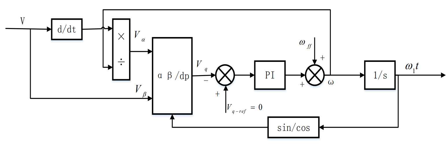
This article uses a single-phase phase-locked loop scheme based on differential virtual two-phase to make the phase angle of the solar inverter output current the same as that of the grid voltage. The control structure is shown in Figure 5.
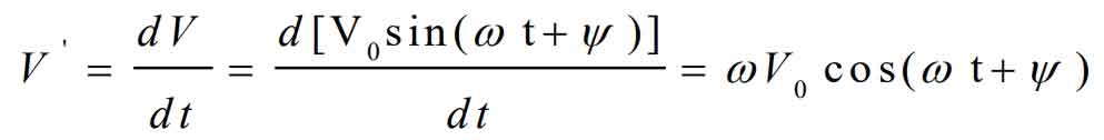
The output voltage of the solar inverter is V=V0Sin(ωt+ψ), and its derivative with respect to time is:
The values of Vd and Vq are obtained by using the transformation formulas between α, β, and d, q, and then the value of Vq is set to zero by using a PI regulator.As shown in Figure 4, when the projection of the given voltage value on the q-axis is zero, it is in phase with the grid voltage, with a phase angle of ωt(θ).
As this article focuses on the household-sized small inverters proposed by the “Solar Roof Program”, only the single-phase case needs to be studied. Figure 4 shows the relationship between the output current of the solar inverter and the grid voltage.
Among them,
I—indicates the output current of solar inverter;
Ugrid – represents the grid voltage;
Id—represents the projection of the solar inverter output current I on the d-axis;
Iq—represents the projection of solar inverter output current I on the q-axis;
θ—indicates the phase angle of the grid voltage.
The output voltage of a solar inverter is V=V0Sin(ωt+ψ), which is differentiated with respect to time, yielding:
PI feedback control is used to make Iq equal to 0, and its control structure is shown in Figure 6.
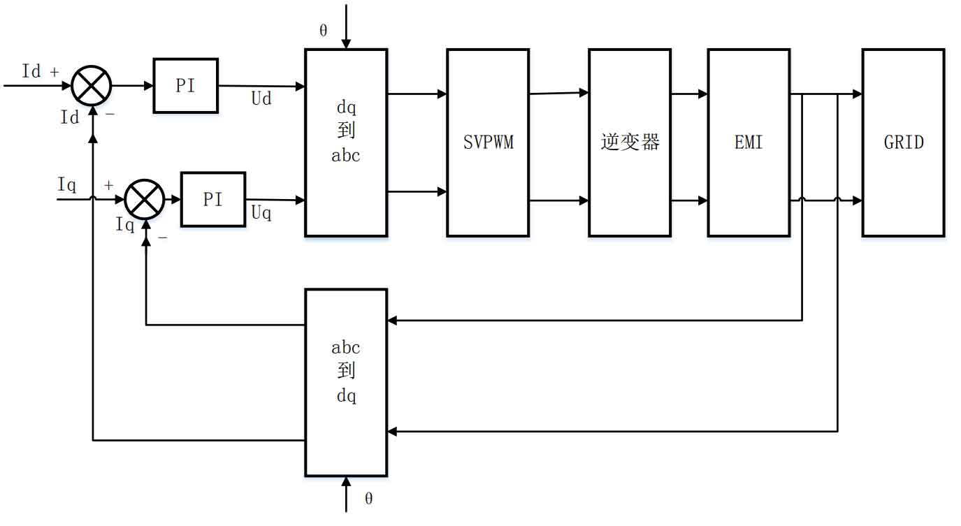
The corresponding relationship between d, q and a, b, c is:
According to the power formula:
P=U*I
Where, P represents the power feedback from the solar inverter to the grid;
U – indicates the output voltage of the solar inverter;
I—indicates the current of solar inverter inputting to the grid.
As the solar inverter is a household solar inverter based on the “Solar Roof Program”, the output voltage is constant at 220V, so the current input to the grid from the solar inverter is proportional to the load (the power fed back to the grid). When the load changes, I changes accordingly, and ultimately the output current of the solar inverter is made in phase with the grid voltage through a phase-locked loop and PI control.
When the solar inverter outputs current I, due to its single-phase nature, it can be decomposed into Id and Iq on the d and q axes.The current signal is converted into a voltage signal through a PI controller, and the change in voltage signal is used to regulate the change in current.The adjusted output voltage signal is then transformed through a space vector coordinate system to convert the d and q direction signals to the a, b, and c axes (the θ angle is given).The converted a, b, and c signals are then passed through the solar inverter’s interleaved flyback circuit and full bridge circuit, and then through an electromagnetic interference filter before being sent to the grid.During the process of sending it to the grid, a negative feedback regulation is involved. The current value output by the electromagnetic interference filter is fed back to the d and q axes through the coordinate transformation from the a, b, and c coordinate system to the d and q axes, in order to regulate the solar inverter so that its output current value is in phase with the grid voltage.
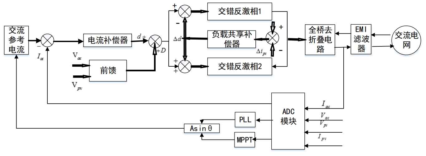
5. Compensator design
The control structure of solar micro-inverters is shown in Figure 7, using a feedforward and feedback structure. The internal current loop controller controls the AC current transmitted to the grid under joint power factor.The current loop has a fast response and a wider bandwidth than the external maximum power point tracking power loop.
6. Design of other auxiliary functions
6.1 Limitation of output power
When the system operates continuously for more than one minute at less than 15% of its rated output power, the burst mode will be enabled.The burst mode means that the system will provide three times the maximum power during one complete AC cycle, and then turn off for two complete AC cycles.During the off period, the large-capacity capacitor is charged to provide high-capacity charging for the load in the next burst cycle.
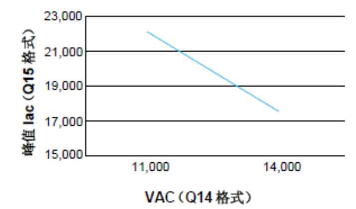
In order to ensure that the output power of the micro solar inverter does not exceed 215W, a software clamp is specially designed to allow the maximum output current.The peak output current of the solar inverter can be determined by the following formula:
y=-1.567x+39530
Converting 1.567 to Q14 format, we obtain Figure 8:
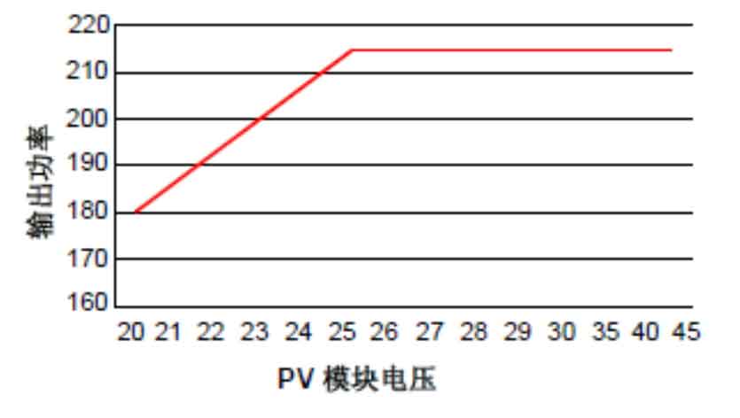
To prevent the saturation of the flyback transformer in PV modules, the power derating function is used to clamp the output current of the solar inverter.Figure 9 shows the functional relationship between output power derating and input voltage:
6.2 Fault management
The main parameters of the TMS320F28035 monitoring system, such as PV panel power, solar inverter output voltage/current, reference voltage, etc. When any signal exceeds the standard, the system will enter an error state.We can observe the fault type by observing the number of flashes of the LED (LED D27) on the PCB.Table 1 shows the fault types corresponding to the number of flashes of the LED:
| Fault | LED flashing frequency | Serious malfunction |
| PV panel undervoltage/overvoltage | 1 | |
| Inverters under/over frequency | 2 | |
| VAC undervoltage/overvoltage | 3 | |
| Lac overcurrent iridium | 4 | Y |
| Flyback overcurrent (ADC/CMP) | 5 | Y |
| Superheat | 6 | |
| Drive power supply overvoltage/undervoltage | 7 | |
| Flyback output voltage (CMP) | 8 | Y |
| 2.5V reference overvoltage/undervoltage | 9 | |
| AC current offset | 10 | |
| Hardware zero crossing fault | 11 |
The on-chip analog comparator is used to implement flyback overvoltage protection and overcurrent protection.When a flyback overvoltage occurs, an analog comparator interrupt will be generated, which disables the PWM output through the PWM rewrite function and sets a critical fault flag.When a flyback overcurrent occurs, the PWM will be locked for 20ns, generating a comparator interrupt to indicate the fault and setting a critical fault flag.
7. Summary
This article mainly introduces the software architecture of the single-phase photovoltaic grid-connected controller, including the state machine, device peripheral configuration, maximum power point tracking algorithm, compensator design, and other auxiliary functions.Among them, the state machine section focuses on the interrelationships between the three states of system error, system startup, and daytime mode.The maximum power point tracking algorithm mainly includes the following two methods: disturbance observation method and incremental conductance method.The compensator design mainly includes: the design of the current loop compensator, the design of the feedforward compensator, and the design of the load sharing compensator.Other auxiliary functions mainly include: the design of the phase-locked loop, fault management, and the limitation of the input power size.