
In recent years, perovskite solar cells have garnered significant attention in both academic and industrial sectors due to their exceptional photovoltaic performance and solution processability. The theoretical efficiency limit of perovskite solar cells can reach up to 43%, with laboratory efficiencies already surpassing 30%. Moreover, their compatibility with solution-based processing techniques, which eliminate the need for high-temperature treatments and high-vacuum equipment, presents a substantial cost advantage. The large-scale, high-quality fabrication of perovskite thin-film active layers, along with functional layers such as electron transport layers, hole transport layers, and insulating layers, is crucial for the commercial application of perovskite solar cells. Various printing and coating technologies, including blade coating, inkjet printing, slot-die coating, spray coating, and screen printing, have been employed for the preparation of perovskite films and solar cell modules.
Among these techniques, screen printing stands out due to its wide applicability, simple equipment and processes, ease of patterning, low cost, high efficiency, strong ink adaptability, and adjustable film thickness. For perovskite solar cells, all functional layers—including the perovskite active layer, mesoporous/compact electron transport layer, carbon electrode, insulating layer, and hole transport layer—can now be fabricated using screen printing. The concept and realization of fully screen-printed perovskite solar cells highlight the immense potential and development prospects of screen printing in this field. In this article, I will discuss the latest advancements in screen printing for perovskite solar cells, address the current challenges, and explore future trends.
Basic Structure of Perovskite Solar Cells
The structure of perovskite solar cells can be broadly classified into mesoporous and planar configurations. Key components include the transparent conductive substrate, electron transport layer, perovskite active layer, hole transport layer, and metal counter electrode. The transparent conductive substrate typically consists of glass or other transparent materials coated with indium-doped tin oxide (ITO) or fluorine-doped tin oxide (FTO) transparent conductive oxide (TCO) films. These substrates offer high light transmittance and electrical conductivity, facilitating light introduction and photogenerated carrier collection. The electron transport layer (ETL) commonly employs inorganic semiconductors like zinc oxide or titanium dioxide, known for their excellent chemical stability and electron mobility, to transport electrons from the perovskite active layer to the transparent conductive electrode. The perovskite active layer, with its ABX3 crystal structure (where A is an organic cation, B is a metal ion, and X is a halide group), serves as the core for photoelectric conversion. It exhibits high light absorption coefficients and carrier mobility, enabling efficient photon absorption and electricity generation. The hole transport layer (HTL) uses materials such as Spiro-OMeTAD or PEDOT:PSS, which possess superior hole mobility, to block electrons while effectively extracting and transporting photogenerated holes. The metal counter electrode, made of gold, silver, or aluminum, reflects transmitted photons back to the perovskite active layer for reabsorption and collects photogenerated charges to connect with external circuits.
The general formula for the perovskite structure is expressed as:
$$ABX_3$$
where A represents organic cations like methylammonium (MA+) or formamidinium (FA+), B denotes metal ions such as lead (Pb2+) or tin (Sn2+), and X is a halide anion like iodide (I−), bromide (Br−), or chloride (Cl−). The photoconversion efficiency (PCE) of a perovskite solar cell can be calculated using the following equation:
$$\text{PCE} = \frac{J_{sc} \times V_{oc} \times FF}{P_{in}}$$
where \(J_{sc}\) is the short-circuit current density, \(V_{oc}\) is the open-circuit voltage, \(FF\) is the fill factor, and \(P_{in}\) is the incident light power density.
Screen Printing Process
Screen printing is a technique that involves transferring ink through the open mesh areas of a screen onto a substrate under the pressure of a squeegee. The screen consists of a mesh where the image areas are permeable to ink, while the non-image areas are blocked. During printing, ink is applied at one end of the screen, and a squeegee moves across the screen, applying pressure to force the ink through the mesh onto the substrate, thereby transferring the pattern. By adjusting parameters such as ink properties (e.g., solid content, composition, viscosity), screen parameters (e.g., mesh count, wire diameter, emulsion thickness), squeegee parameters (e.g., pressure, angle, hardness), and printing conditions (e.g., speed, number of passes), along with substrate treatment and environmental control, the thickness and quality of the printed film can be precisely controlled. Screen printing is compatible with various inks, including water-based, oil-based, and those containing coarse particles, and it can be applied to rigid and flexible substrates like glass, plastic, and paper, as well as flat, curved, or spherical surfaces. Its simplicity in equipment and process makes it highly advantageous for low-cost, high-efficiency, large-area manufacturing.
The flow behavior of ink during screen printing can be described by the Herschel-Bulkley model, which accounts for shear-thinning or shear-thickening properties:
$$\tau = \tau_0 + K \dot{\gamma}^n$$
where \(\tau\) is the shear stress, \(\tau_0\) is the yield stress, \(K\) is the consistency index, \(\dot{\gamma}\) is the shear rate, and \(n\) is the flow behavior index. For optimal printing, the ink viscosity \(\eta\) should be tailored to the screen mesh and substrate, often following the relationship:
$$\eta = \frac{\tau}{\dot{\gamma}}$$
Table 1 summarizes key parameters in screen printing for perovskite solar cells and their typical ranges.
| Parameter | Description | Typical Range |
|---|---|---|
| Mesh Count | Number of threads per inch | 100-400 |
| Ink Viscosity | Resistance to flow (Pa·s) | 1-50 |
| Squeegee Pressure | Force applied by squeegee (N) | 10-100 |
| Printing Speed | Speed of squeegee movement (mm/s) | 10-100 |
| Film Thickness | Thickness of printed layer (μm) | 0.5-20 |
Screen Printing of Functional Layers in Perovskite Solar Cells
The development of specialized inks and optimization of printing processes are central to the screen printing of functional layers in perovskite solar cells. Below, I detail advancements in screen printing for the electron transport layer, perovskite active layer, and hole transport layer, with a focus on fully screen-printed devices.
Electron Transport Layer
Titanium dioxide (TiO2) is a widely used material for the electron transport layer in perovskite solar cells. In screen printing, the separation mechanism of TiO2 ink between the screen and substrate is critical for producing defect-free, smooth, and high-performance films. Studies have shown that adjusting the rheological properties of the ink, such as viscosity and elasticity, can significantly influence ink transfer and film morphology. For instance, high-speed imaging has been used to evaluate inks with different solvent dilutions and rheological behaviors, revealing that optimized viscosity and elasticity improve TiO2 film uniformity and enhance the wetting properties of perovskite precursors. This optimization leads to a notable increase in open-circuit voltage and fill factor, boosting the power conversion efficiency of large-area perovskite solar cell modules by over 10%.
The electron transport in TiO2 can be modeled using the drift-diffusion equation:
$$J_n = q \mu_n n E + q D_n \frac{dn}{dx}$$
where \(J_n\) is the electron current density, \(q\) is the elementary charge, \(\mu_n\) is the electron mobility, \(n\) is the electron concentration, \(E\) is the electric field, and \(D_n\) is the electron diffusion coefficient. Table 2 compares different electron transport layer materials and their properties relevant to screen printing.
| Material | Bandgap (eV) | Electron Mobility (cm²/V·s) | Compatibility with Screen Printing |
|---|---|---|---|
| TiO2 | 3.2 | 0.1-1 | High |
| ZnO | 3.3 | 1-10 | Moderate |
| SnO2 | 3.6 | 10-100 | High |
Perovskite Active Layer
Screen printing of the perovskite active layer has been challenging due to the low viscosity of traditional organic solvent-based perovskite inks, which are unsuitable for the process. However, innovative approaches, such as using tunable ionic liquid-based perovskite inks, have enabled precise control over film formation and facilitated fully screen-printed perovskite solar cells. These inks offer adjustable viscosity and composition, allowing for the deposition of high-quality perovskite films. For example, research has demonstrated that ionic liquid inks can achieve uniform perovskite crystallization within mesoporous scaffolds, resulting in devices with efficiencies up to 17% and improved stability. The crystallization kinetics of perovskite films can be described by the Avrami equation:
$$X(t) = 1 – \exp(-k t^n)$$
where \(X(t)\) is the fraction of crystallized material at time \(t\), \(k\) is the rate constant, and \(n\) is the Avrami exponent. Table 3 outlines typical ink formulations for screen-printed perovskite active layers.
| Ink Component | Function | Concentration Range |
|---|---|---|
| Perovskite Precursor (e.g., MAPbI3) | Light absorption and charge generation | 1-2 M |
| Solvent (e.g., DMF, DMSO) | Dissolution and viscosity control | 50-90 wt% |
| Additive (e.g., ionic liquids) | Morphology and stability enhancement | 1-10 wt% |
Counter Electrode and Other Functional Layers
To address issues like metal atom migration in noble metal electrodes (e.g., Au, Ag), screen-printable carbon-based counter electrodes have been developed. These electrodes offer excellent stability and are compatible with the screen printing process. In one approach, a conductive substrate is sequentially screen-printed with layers of TiO2 nanocrystals, ZrO2 insulation, and carbon counter electrode, followed by infiltration of the perovskite active material. This method has yielded devices with efficiencies around 18%, demonstrating the viability of carbon electrodes in perovskite solar cells. The sheet resistance \(R_s\) of the electrode can be calculated as:
$$R_s = \frac{\rho}{t}$$
where \(\rho\) is the resistivity and \(t\) is the thickness. For large-area modules, the total resistance \(R_{total}\) is given by:
$$R_{total} = R_s \frac{L}{W}$$
where \(L\) is the length and \(W\) is the width of the electrode.
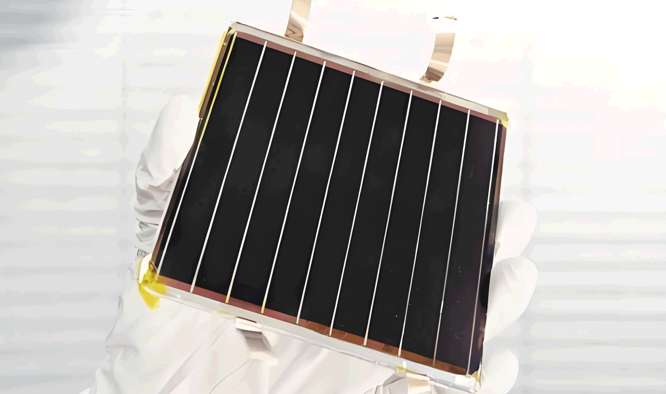
Fully Screen-Printed Perovskite Solar Cells
The concept of fully screen-printed perovskite solar cells has been realized, showcasing the technology’s potential for scalable manufacturing. This approach involves screen printing all functional layers—electron transport layer, perovskite active layer, hole transport layer, and counter electrode—on a single substrate. Advances in ink design and process optimization have enabled efficiencies exceeding 17% in lab-scale devices, with ongoing efforts to scale up to industrial levels. The overall device performance can be analyzed using the diode equation:
$$J = J_0 \left( \exp\left(\frac{qV}{nkT}\right) – 1 \right) – J_{ph}$$
where \(J_0\) is the reverse saturation current density, \(V\) is the voltage, \(n\) is the ideality factor, \(k\) is Boltzmann’s constant, \(T\) is the temperature, and \(J_{ph}\) is the photocurrent density. Challenges in fully screen-printed devices include achieving uniform layer thickness, minimizing interfacial defects, and ensuring long-term stability under operational conditions.
Challenges and Future Perspectives
Despite progress, several challenges remain for screen-printed perovskite solar cells. The uniformity of functional layers over large areas needs improvement to enhance efficiency and reproducibility. Interface engineering is crucial to reduce charge recombination and improve carrier extraction. Stability issues, such as degradation under moisture, oxygen, and light exposure, require the development of advanced encapsulation materials and techniques. Additionally, for applications in wearable electronics, lightweight and flexible designs must be optimized to withstand bending and mechanical stress. Future research should focus on novel ink formulations, in-situ monitoring during printing, and integration with roll-to-roll processes for high-throughput production.
The economic viability of screen-printed perovskite solar cells can be assessed using the levelized cost of electricity (LCOE) formula:
$$\text{LCOE} = \frac{\sum_{t=1}^{n} \frac{I_t + M_t}{(1+r)^t}}{\sum_{t=1}^{n} \frac{E_t}{(1+r)^t}}$$
where \(I_t\) is the investment cost in year \(t\), \(M_t\) is the maintenance cost, \(E_t\) is the energy output, \(r\) is the discount rate, and \(n\) is the lifetime of the system.
Conclusion
In summary, screen printing has emerged as a promising technique for the fabrication of perovskite solar cells, offering advantages in cost, scalability, and versatility. Recent advancements in ink development and process control have enabled the screen printing of all functional layers, leading to fully printed devices with competitive efficiencies. However, challenges related to uniformity, stability, and flexibility must be addressed to accelerate commercial adoption. Ongoing research and innovation in screen printing technology will play a pivotal role in realizing the full potential of perovskite solar cells for sustainable energy solutions.