
Solar energy is no longer an emerging technology, but a technology that is undergoing significant technological changes and is becoming increasingly mature. We are moving towards grid parity, where the cost of solar energy is comparable to that of traditional energy generation, and the goal of improving the composition of traditional energy generation is getting closer, as the process of converting direct current in panels into usable alternating current becomes more efficient and cost-effective.
However, although the prices of solar panels have significantly decreased in recent years, the next wave of solar development will be driven by new technologies in power converter systems. The rise of advanced and complex multi-level power switch topologies will be based on silicon carbide (SiC) and gallium nitride (GaN) materials, coupled with higher operating voltages (up to 1600 VDC), to achieve faster power switching and significantly improve performance compared to traditional systems. A higher switching frequency means that the passive components of the power converter, such as induction coils and capacitors, can be significantly reduced in size, thereby reducing weight and cost. These two are key advantages for further expansion of the solar energy market. The new power switch topology is driving the transformation of devices that can provide relevant control and support. Smaller and faster systems require improvements in the entire power conversion signal chain, faster processing, and better device integration. However, as modern solar photovoltaic inverters become smaller and smaller, these innovations exacerbate the challenge of addressing the important safety issues inherent in power conversion. That is to say, due to the downsizing of these systems, the physical isolation of hazardous voltages becomes more complex.
In addition, official security certification is a requirement faced by all developers. Many regulations regarding safe disconnection (and reconnection) must be followed. The speed at which the system must respond, how to handle power outages, quick disconnections, and arc detection must all be addressed. In many cases, the solutions vary for each country/region. Due to the increased development time (cost) associated with certification, certified devices and methods are highly attractive and require sufficient flexibility to adapt to multiple evolving regional safety regulations.
Fortunately, these issues can be easily solved by using a power solar photovoltaic inverter platform that can integrate advanced hybrid signal control processors and be surrounded by complementary isolation current detection and gate driver technology.
1.Fault safety of solar photovoltaic inverters
For safety critical applications such as AC monitors and isolators for solar photovoltaic inverters, in addition to monitoring equipment, safety standards require redundant monitoring components to ensure single fault safety. In traditional solar photovoltaic inverters, this is achieved by adding a monitoring processor to the system, which acts as a redundant monitoring element and then controls relay K2. In Figure 1, in traditional solar photovoltaic inverter control hardware, a separate monitoring processor is responsible for redundant safety component K2 and related monitoring. Both processors run some security software and communicate through standard I/O facilities.
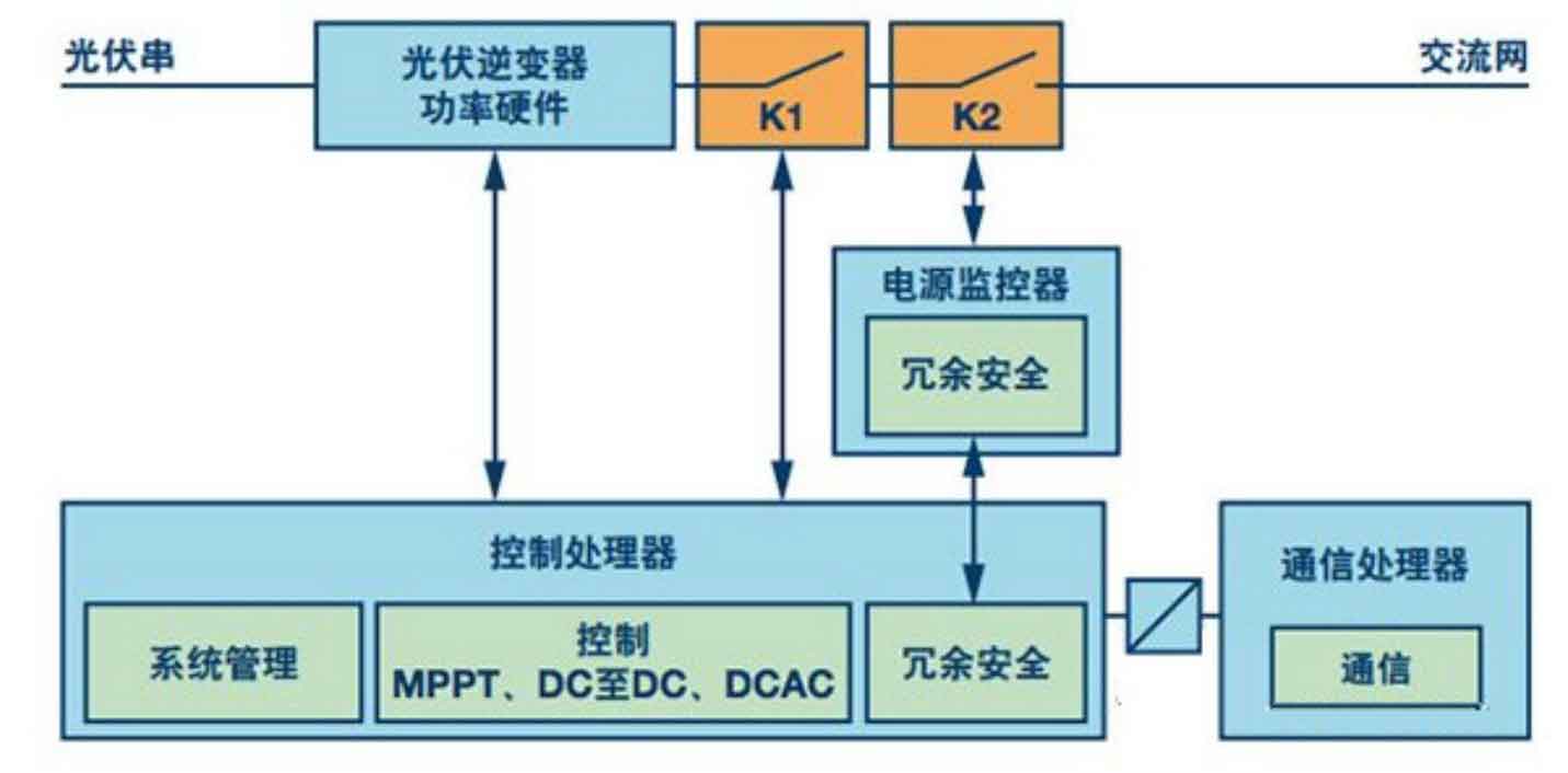
It is easy to see that this significantly increases the overall cost of system control hardware, as although the monitoring components actually include processors with good performance requirements, additional supporting infrastructure must also be added. On the other hand, the separation of redundant components in this configuration is obvious, so it is an easy to understand security layout when conducting qualified audits by security agencies.
Although solar photovoltaic inverter manufacturers strive to improve the performance of solar photovoltaic inverters, the global market’s demand for reducing the total operating cost of solar photovoltaic systems is constantly putting pressure on manufacturers and forcing them to strengthen research to improve the topology of solar photovoltaic inverters and reduce the cost of safety critical components of solar photovoltaic inverters. Therefore, in order to minimize costs as much as possible, the redundant monitoring components of safety isolators have become components that should be strictly audited.
2. Advantages of dual core design
The desire to simultaneously simplify and enhance the operation of solar photovoltaic inverters has driven the development of a series of innovative hybrid signal control processors, the ADSP-CM41x series. The core of ADSP-CM41x design is the breakthrough independent dual core security concept, which can integrate security redundancy and functionality into a single chip. This unprecedented architecture does not require external monitoring components (which is the current standard), which can save a lot of development time and system costs. The all-new ADSP-CM41x solves today’s power conversion problems through a set of features specifically designed for renewable energy conversion system requirements, including integrated and optimized hardware accelerators, aimed at improving kernel processing capabilities. In addition, the onboard arc fault detection function of the equipment can simplify design and enhance safety through intelligent decision-making, thereby improving reliability and accuracy. By adding an independent M0 monitoring kernel to the main M4 control kernel on a single chip, the design of a single fault tolerant system with redundant monitoring and control signal paths has been significantly simplified, while reducing overall system costs. Figure 2 shows that the dual core design greatly simplifies the design of redundant security components by integrating independent M0 monitoring cores. The processor communicates through a dedicated email system, including the transmission of heartbeat signals.
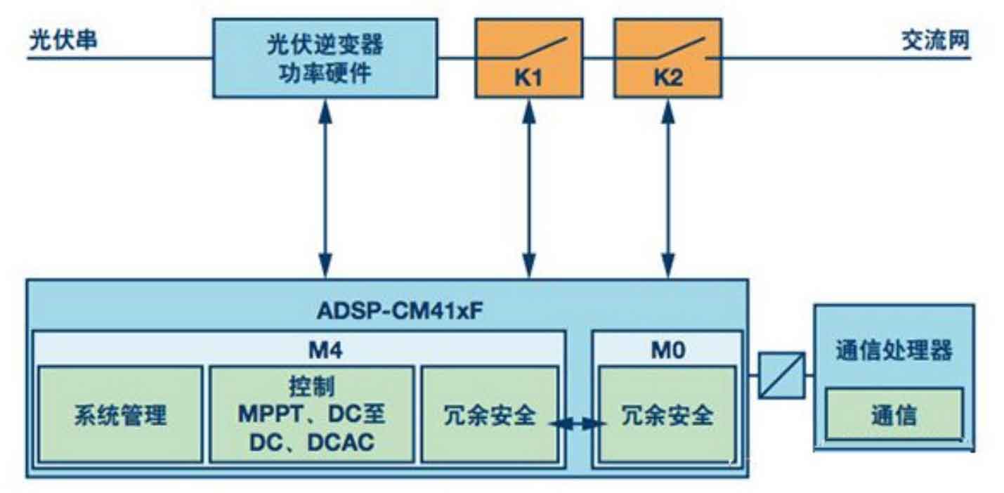
Although the M0 and M4 cores are on the same wafer, the cost is the least from a security perspective. But the kernel is physically separated through innovative system architecture design, and the process parameters obtained through redundancy can be independently checked and verified through inter processor communication through dual port RAM mailboxes.
3. Code Security
In addition to physical power supply safety, it is important to be cautious to ensure that the algorithms running these systems are correctly interpreted; The working state where process disruption can lead to reduced safety. In addition, it is advantageous to use a mailbox communication system that can separate the functions of the processor core to isolate communication between processors. The mailbox system allows any kernel to isolate reading/writing data at any time, rather than directly exchanging signals for sending and receiving communication. For code security, the M4 kernel has 1 MB of flash memory and up to 160 kB SRAM, while the M0 has 32 kB SRAM. M4 and M0 processors L1 SRAM, flash memory, and mailbox storage are protected with zero wait state SECDED ECC, and native protection of 32-bit memory elements. Writing 8-bit and 16-bit data in appropriate places will cause automatic backend reading, modification, and writing of ECC updates, usually without observable processor pauses. Refreshing auxiliary hardware can periodically handle single bit errors. Multi bit error detection can also be used to trigger interrupts and/or faults. In addition, for error detection, the cyclic redundancy check (CRC) hardware module is used to calculate the CRC of the data block. It is based on the CRC32 engine and can calculate the CRC value of the 32-bit data words passed to it. Specifically, CRC units can be used to validate flash memory content, i.e. constant data blocks (text or code) in SRAM.
As an example of how to use a dual core design to achieve AC power grid monitoring using a dual core mixed signal control processor, let’s take a look at the working principle of AC power grid monitoring in solar photovoltaic inverters. AC power grid monitoring mainly includes two functions: frequency monitoring and voltage monitoring.
For frequency monitoring, it is necessary to strictly allow time based measurements, which may be difficult to achieve when using RC oscillators as backup time bases. Therefore, the processor uses a single oscillator or crystal oscillator (XTAL) as the main system clock (SYSCLK) input, and uses other XTAL on M0 to monitor the drift of the main clock source through the mailbox. Clock faults on the SYSCLK line, except for drift, are directly handled by the internal oscillator comparator unit (OCU). It uses an external low-frequency oscillator (LFO) to detect various conditions, such as clock disappearance and clock frequency overruns, and can generate several events to notify the processor of related violations. When a fault event is detected, the clock malfunction signal (CLKNG) can be configured to place the chip in a reset state, and it can also initialize the GPIO pin safety state mechanism.
AC voltage monitoring must ensure that the phase voltage is within the required tolerance range and can also be used for functional self testing of two isolation switch relays. To achieve single fault voltage withstand monitoring, the analog front-end (AFE) of the processor includes two separate ADCs, each with its own ADC controller, reference voltage, and multiple power paths. Of course, one ADC is controlled by M4 and the other by M0 to achieve fully redundant voltage measurement and integrity check of the mailbox system. In addition, before connecting the solar photovoltaic inverter to the grid, the onboard DAC can be used for all devices that individually apply AFE signal chains internally.
4. Platform examples of solar photovoltaic inverters
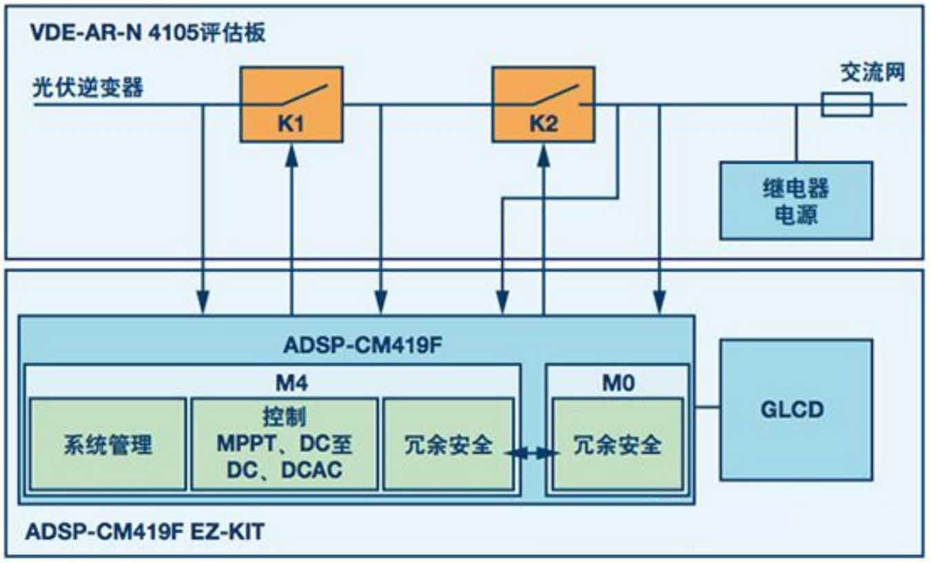
In addition to hybrid signal processors, there are many other key components in photovoltaic systems that need to be used together to safely communicate, control, and transmit data and current. Figure 3 shows the VDE-AR-N-4105 technology demonstration device, which includes the VDE-AR-N-4105 evaluation board and ADSP-CM419FEZ-KIT. The design adopts the concept of redundant signal paths, including redundant references, ADC and XTAL, as well as internal oscillators and voltage monitoring units and the mailbox system between the processor, allowing for the complete elimination of other external monitoring components from the monitoring system. The graphical LCD provides all relevant status information at a glance, and the complete calibration cycle of the entire system can be performed with just one click of a button. This unit is equipped with widely validated software packages. The technical demonstration device adopts two series power relays that constitute the main AC power supply path, as well as four independent high-precision isolated voltage measurement channels for redundant monitoring of AC power supply voltage, solar photovoltaic inverter output, and relay to relay voltage in single-phase systems.
The prospects for the solar energy industry are bright, but continuous progress is not enough. The intelligent integration of various technologies at the entire platform level will ensure the efficiency and safety of power converter design. Each device must be designed specifically based on the safety, efficiency, and cost requirements of the energy market. Providing a complete and robust platform, not just devices, will allow manufacturers of future power converter products to create clean, safe, and cost-effective systems.
5. Conclusion
Due to cost reduction efforts that can easily weaken the required level of system security, it is necessary to consider integrating monitoring components as a second processor onto the same silicon chip as the main processor to address potential security issues. Another consideration is the minimum requirements that such dual core processors must meet in order to comply with regulatory standards for safe disconnection of AC power on solar photovoltaic inverters. This series is equipped with a set of features specifically designed for the power conversion requirements of renewable energy conversion systems, including all necessary safety components, to form an AC circuit breaker that fully meets safety requirements.
In addition, to support security, the power conversion platform is based on its digital isolator technology and integrates gate drivers and current sensors. The digital isolator utilizes a low stress thick film polyimide insulation layer to achieve thousands of volts of isolation, which can be integrated with standard silicon ICs to form single channel, multi-channel, and bidirectional configurations.