
The working circuit of a string solar inverter is mainly divided into a front-end DC/DC boost circuit and a back-end DC/AC inverter circuit. For a series photovoltaic system with a voltage level of 1000 V, a simple two-level Boost circuit can be selected for the front-end DC/DC boost scheme to meet the design requirements. The power switch device adopts Si IGBT module, which is convenient to select and affordable in price. However, for a series photovoltaic system with a voltage level of 1500 V, if a two-level Boost circuit is used, it is necessary to choose Si IGBT modules or SiC MOSFET modules with higher voltage withstand levels, which will greatly increase product costs and circuit losses. A three-level Boost circuit with advantages such as reducing switch device voltage stress and increasing switching frequency can solve this problem. The common three-level Boost circuits include symmetrical three-level Boost and flying capacitor three-level Boost. Among them, the flying capacitor three-level Boost has advantages such as frequency doubling characteristics and low demand for magnetic components [6-8], and is suitable for string solar inverters. Therefore, it is of great significance to study and design the flying capacitor three-level Boost circuit.
This article will analyze in detail the working principle of the flying capacitor three-level Boost from the aspects of circuit structure and working mode; Simultaneously design a fly over three-level Boost main circuit scheme suitable for mainstream photovoltaic panel characteristics, calculate the input filtering inductance, input filtering capacitance, fly over capacitance, power switch device losses and other parameters of the fly over Boost main circuit, and propose a control strategy for the fly over Boost circuit under dynamic working conditions; By simulating and verifying the effectiveness and accuracy of the circuit parameter design method and device selection, a flying boost circuit parameter design method is provided for a series solar inverter with a voltage level of 1500 V.
1. Analysis of the working principle of the Flyover Boost circuit
1.1 Flyover three-level Boost circuit structure
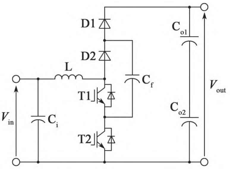
The flying three-level Boost circuit is shown in Figure 1, which includes an input filtering capacitor Ci, an input filtering inductor L, switching transistors T1 and T2, power diodes D1 and D2, a flying capacitor Cf, Vin as the input voltage, and Vout as the output voltage. During normal operation, the voltage of the flying capacitor Cf is controlled at approximately half of the output voltage, i.e. Vout/2, which reduces the withstand voltage of each switching device by about half of the output voltage.
For the convenience of analyzing the working mode of the circuit, the following assumptions are made first:
① The switching devices and inductors and capacitors in the circuit are both ideal devices; ② The voltage of the flying capacitor is maintained at half of the output voltage. In addition, the switch state variable xi of the i-th switching transistor Ti is defined as:
In the formula, a value of 0 for xi represents the disconnection of switch Ti, and a value of 1 represents the conduction of switch Ti.
1.2 Flyover Boost working mode
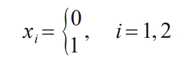
According to the switch states x1 and x2 of switch tubes T1 and T2, four different flying boost operating modes can be combined, which are:

Set S1=(0,1) as mode one, with switch tube T1 disconnected and switch tube T2 conducting; S2=(1,0) is mode two, with switch tube T1 conducting and switch tube T2 disconnected; S3=(0,0) is mode three, and switch tubes T1 and T2 are both disconnected; S4=(1,1) is mode four, and both switch tubes T1 and T2 are conducting. The equivalent circuits of these four working modes are shown in Figure 2 (the blue line in the figure indicates no conduction).
Based on reverse PWM carrier modulation, the switching tubes T1 and T2 of the flyover Boost circuit conduct 180 ° alternately with a duty cycle D. According to the size of the duty cycle D, the working state of the flyover Boost circuit can be divided into two types: when the duty cycle D is ≤ 0.5, the circuit operates in the S1-S3-S2-S3 cycle; When the duty cycle D is greater than 0.5, the circuit operates in the S1-S4-S2-S4 cycle. To study the stable and safe operation of the Flyover Boost under different duty cycles, this article compares and analyzes the two working states.
1.2.1 Working state under duty cycle D ≤ 0.5
The circuit operates in S1-S3-S2-S3 cycles, and the circuit states in each operating mode within one switching cycle T are shown in Figure 3. The specific analysis is as follows:
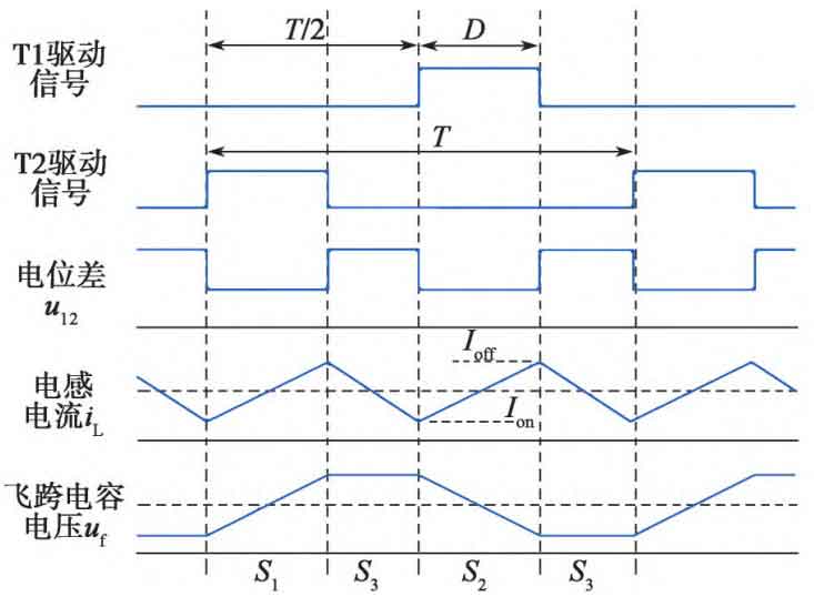
① S1: Duration D · T, T1 tube is disconnected, T2 tube is conductive, current circuit is Vin-L-D2-Cf-T2-Vin, T1 tube is subjected to voltage stress of Vcp=Vout/2, inductance current increases linearly, inductance L stores energy, and flying capacitor Cf stores energy.
② S3: Duration (0.5-D) · T, both T1 and T2 tubes are disconnected, and the current circuit is Vin-L-D21-Vout Vin. The voltage stress borne by T1 tube is Vcp=Vout/2, and the voltage stress borne by T2 tube is Vout Vcp=Vout/2. The inductance current decreases linearly, and the inductance L releases energy, while the energy of the flying capacitor Cf remains unchanged.
③ S2: Duration D · T, T1 tube conducts, T2 tube disconnects, current circuit is Vin-L-T1-Cf-D1 Out Vin, T2 tube bears voltage stress of Vout Vcp=Vout/2, inductor current increases linearly, inductor L stores energy, and flyover capacitor Cf releases energy.
④ S3: Duration (0.5-D) · T, the circuit status is consistent with the previous ②.
1.2.2 Working state with duty cycle D>0.5
The circuit operates in S1-S4-S2-S4 cycles, and the circuit states in each operating mode within one switching cycle T are shown in Figure 4. The specific analysis is as follows:
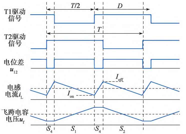
① S1: Duration (1-D) · T, T1 tube is disconnected, T2 tube is conductive, and the current circuit is Vin-L-D2-Cf-T2-Vin. The voltage stress borne by T1 tube is Vcp=Vout/2, and the inductance current linearly decreases. The inductance L releases energy, and the flying capacitor Cf stores energy.
② S4: Duration (D-0.5) · T, both T1 and T2 tubes are conducting, and the current circuit is Vin-L-T1-T2-Vin. The inductance current increases linearly, the inductance L stores energy, and the energy of the flying capacitor Cf remains unchanged.
③ S2: Duration (1-D) · T, T1 tube conducts, T2 tube disconnects, current circuit is Vin-L-T1-Cf-D1 Out Vin, T2 tube bears voltage stress of Vout Vcp=Vout/2, inductor current linearly decreases, inductor L releases energy, and flying capacitor Cf releases energy.
④ S4: Duration (D-0.5) · T, the circuit status is consistent with the previous ②.
The potential difference between the collector of T1 tube and the emitter of T2 tube is defined as u12=u1C-u2E. The comparison results of the two working modes are shown in Table 1.
| D ≤ 0.5 | D ≤ 0.5 | D ≤ 0.5 | D ≤ 0.5 | D > 0.5 | D > 0.5 | D > 0.5 | D > 0.5 | |
| Working mode | S1 | S2 | S3 | S4 | S1 | S2 | S3 | S4 |
| Duration | D·T | D·T | (0.5-D)·T | (1-D)·T | (1-D)·T | (D-0.5)·T | ||
| T1 pipe pressure drop | Vout/2 | 0 | Vout/2 | Vout/2 | 0 | 0 | ||
| T2 pipe pressure drop | 0 | Vout/2 | Vout/2 | 0 | Vout/2 | 0 | ||
| Potential difference u12 | Vout/2 | Vout/2 | Vout | Vout/2 | Vout/2 | 0 | ||
| Inductive current variation | increase | increase | reduce | reduce | reduce | increase | ||
| Inductive energy variation | storage | storage | release | release | release | storage | ||
| Energy variation of flying capacitor | storage | release | unchanged | storage | release | unchanged |
According to Table 1, regardless of the operating mode, switch tubes T1 and T2 can only withstand half of the bus output voltage at most, and the input filtering inductor current fluctuation frequency is approximately twice the switching frequency change; U12 only has two voltage values. When D ≤ 0.5, u12 is equal to Vout or Vout/2, and when D>0.5, u12 is equal to Vout/2 or 0, which can reduce the high-frequency AC component of the inductor voltage.
2. Main circuit design and selection of switching devices
To meet the requirements of mainstream photovoltaic panel parameters and string solar inverter applications, the parameter requirements for the fly across three-level Boost circuit are as follows: maximum input current is 60 A; The full load input voltage range is DC 800-1 300V; The rated output voltage is 1300 V; The switching frequency is 16 kHz.
2.1 Selection of Power Semiconductor Devices
1) According to the analysis results in Section 1.1, the rated voltage Vce and rated current Ice of the IGBT are:
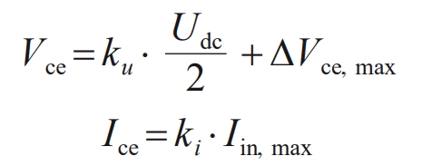
In the formula: ku is the overvoltage coefficient, taken as 1.15; Udc is the output DC bus voltage; Δ Vce, max is the turn off overvoltage, taken as 200 V; Ki is the current peak coefficient, taken as 1.1; Iin, max is the maximum input current, which is the single circuit short-circuit current.
The calculation shows that Vce=947.5 V and Ice=66 A. Select the power semiconductor module parameters of a certain brand that meet the requirements of this parameter, as shown in Table 2.
| Parameter Name | Parameter values |
| IGBT rated voltage/V | 950 |
| Rated current of IGBT/A | 145 |
| IGBT maximum current/A | 400 |
| Diode rated voltage/V | 1 200 |
| Diode rated current/A | 72 |
| Maximum diode current/A | 273 |
| IGBT junction thermal resistance/(K · W-1) | 0.34 |
| Diode junction thermal resistance/(K · W-1) | 0.57 |
| Working temperature/℃ | -40~150 |
2) Based on the selected module loss and junction temperature calculation
To verify that the actual operating temperature of the selected module meets the requirements, calculate its loss and junction temperature. When the input voltage of the Flyover Boost circuit is 800 V, the peak to peak value of the inductor ripple current can be calculated as 0.6 times the maximum input current. From Figure 3 and Figure 4, it can be seen that the turn-on current of T1 and T2 is Iin, max -0.6 Iin, max/2=42 A, and the turnoff current Ioff is Iin, max+0.6 Iin, max/2=78 A. According to the on/off loss curve of the device, it can be seen that at 125 ℃, the on/off loss of the IGBT at 42 A is 1.1 mJ, the on/off loss at 78 A is 3.6 mJ, the on/off voltage drop of the IGBT is 1.35 V, and the on/off voltage drop of the diode is 1.85 V. Combined with the module thermal resistance parameters, the chip loss and temperature rise are calculated as shown in Table 3.
| Parameter Name | Calculated value |
| Single IGBT chip power consumption/W | 102.2 |
| IGBT chip temperature rise/K | 34.75 |
| Single diode chip power consumption/W | 74 |
| Diode chip temperature rise/K | 42.18 |
| IGBT module total power consumption/W | 704.8 |
The calculation of junction temperature is an important step in the application of power devices. The IGBT module of the string solar inverter is closely attached to the surface of the heat sink, and the module junction temperature is mainly composed of the surface temperature of the heat sink and the temperature rise of the chip. Based on engineering experience, the surface temperature of the heat sink is generally set at 80 ℃. Combined with the chip temperature rise calculation results in Table 3, it can be seen that the highest junction temperature of the module is 122.18 ℃, which is lower than the maximum operating temperature of the module in Table 2 by 150 ℃. Therefore, the selected power semiconductor module meets the application requirements.
2.2 Input filtering inductance
The smaller the inductance, the greater the peak to peak value of the inductor ripple current. At this time, the electromagnetic interference problem during switching devices becomes more serious. Therefore, it is necessary to study the trend of peak to peak value changes of the inductor ripple current and use the current limit point as the design basis for input filtering inductance. From Figures 3 and 4, it can be seen that the rise and fall values of the inductor current are equal in each cycle. Taking S3 and S4 as examples, the peak to peak value of the inductor ripple current Δ IL is:
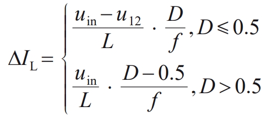
From D=1- uin/uout, it can be concluded that:
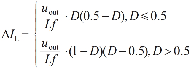
In the formula: uin represents the input voltage; Uout is the output voltage; D is the duty cycle; L is the inductance value; F is the switching frequency.
Calculate the peak to peak value of inductive ripple current Δ The relationship between IL and duty cycle D is shown in Figure 5.
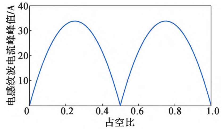
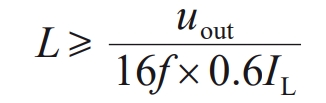
As shown in Figure 5, in a three-level flyover Boost circuit, the duty cycle D=0.25 or 0.75 is the limit point, and the maximum peak to peak value of the inductor ripple current is Δ IL, max=uout/16Lf. Normally, Δ IL, max does not exceed 0.6 times the average inductance current. Therefore, the input filtering inductance satisfies the following equation: IL is the average inductance current. If calculated based on the maximum input current of 60 A, then L ≥ 141 μ H.
Taking L=150 μ H. Substitution Δ IL, max=uout16Lf, the maximum peak to peak value of inductor ripple current can be obtained Δ IL, max=33.86 A.
2.3 Input filtering capacitor
According to Kirchhoff’s law, the input filtering capacitor current is the difference between the input current of the photovoltaic panel (PV) and the ripple current of the inductor. In practical engineering applications, the input filtering capacitor should filter out high-frequency ripple currents as much as possible to prevent ripple currents from flowing back to the battery board. That is, the DC component of the inductor ripple current is provided by the PV, and the AC component is provided by the input filtering capacitor. According to Figures 3 and 4, it can be seen that the ripple frequency of the inductor current is twice the switching frequency. Based on the shunt relationship between the capacitance of the input filtering capacitor and the internal resistance of the power supply, the input filtering capacitor Cin should meet the following requirements:
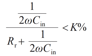
In the formula: angular frequency ω = 2 π f; Rr is the internal resistance of the power supply; K% is the proportion of ripple current flowing back to the battery board, taken as 2%.
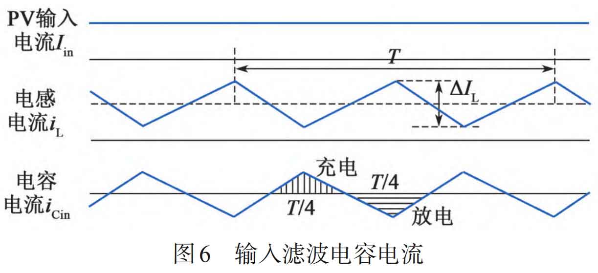
In an ideal situation, the input current of the PV has no ripple, and the input filtering capacitor current is all inductor ripple current. The peak to peak value of the capacitor ripple current is the same as that of the inductor ripple current, with opposite waveform directions. The average current is 0, and the charging and discharging time and charge phase of the capacitor within one cycle are shown in Figure 6. Therefore, the charging amount of the capacitor, Qin, is:
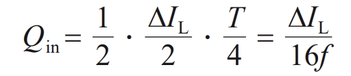
In the formula: T is the minimum period of the switch, which is twice the ripple period of the inductor.
The ripple current of the input filtering capacitor generates a pulsating voltage during the charging and discharging process, which can affect the safety of the capacitor’s operation when the PV input voltage is superimposed. According to the capacitance definition formula, the input filtering capacitor Cin should also meet the following requirements:
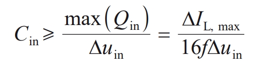
In the formula: Δ Uin is the input capacitor ripple voltage, with a value of 20 V. By combining equations (8) and (10), it can be calculated that the minimum value of Cin is 14 μ F.
2.4 Flyover capacitance
The flying capacitor charges at the average current IL in S1 mode and discharges at the average current IL in S2 mode, resulting in voltage fluctuations when the charging and discharging amounts are equal within one cycle Δ If uf should be less than 10% of the half voltage of the busbar, i.e. 65 V, then the flying capacitor Cf meets the following requirements:
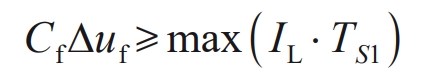
In the formula: TS1 is the duration of S1 state. Due to the different values of TS1 in the cases of D ≤ 0.5 and D>0.5, considering both cases separately, Cf should satisfy equation (12).
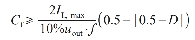
In the formula: IL, max is the maximum average charging current, taken as 60 A. When D=0.5, the value on the right side of equation (12) is the highest, and the flying capacitance Cf ≥ 28.85 μ F. Take 42 μ F.
3. Dynamic control strategy for flying across Boost circuits
To maintain stable operation of the circuit and expect the operating voltage of the switching transistor in the flyover Boost circuit to be lower than its rated voltage, it is necessary to accurately control the input filtering inductor current and flyover capacitor voltage. According to Figure 2, the dynamic equation of the fly over Boost circuit can be listed as follows:
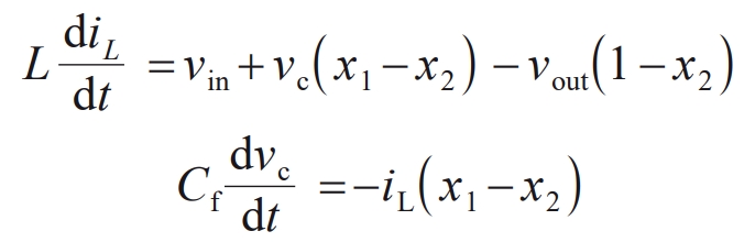
In the formula: iL is the input filtering inductor current; Vin and vout represent the input and output voltages of the Flyover Boost circuit, respectively; VC is the voltage across the flying capacitor. In a stable state, the switching states x1 and x2 of switching tubes T1 and T2 can be regarded as continuous duty cycle input variables, and x1 ≈ x2. The pulse widths of T1 and T2 tubes are basically the same. According to equation (13), ignoring small quantities δ = X1- x2, the input filtering inductor current is mainly controlled by the pulse width of the T2 transistor; According to equation (14), it can be seen that by fine-tuning the pulse width difference between T1 and T2 tubes δ, It can control the voltage of the flying capacitor to the expected value, which is the half voltage of the busbar. As shown in Figure 7, establish the following dynamic control strategy:
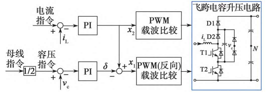
① Amplify the deviation between the input current command value and the input filtering inductor current iL to obtain the pulse width x2 of the T2 transistor;
② Using the half voltage of the busbar as the voltage command value of the flying capacitor, the deviation between the voltage command value of the flying capacitor and the detection value is amplified to obtain the pulse width difference between T1 and T2 tubes δ, The pulse width of T1 tube x1=x2+ δ。
4. Simulation calculation
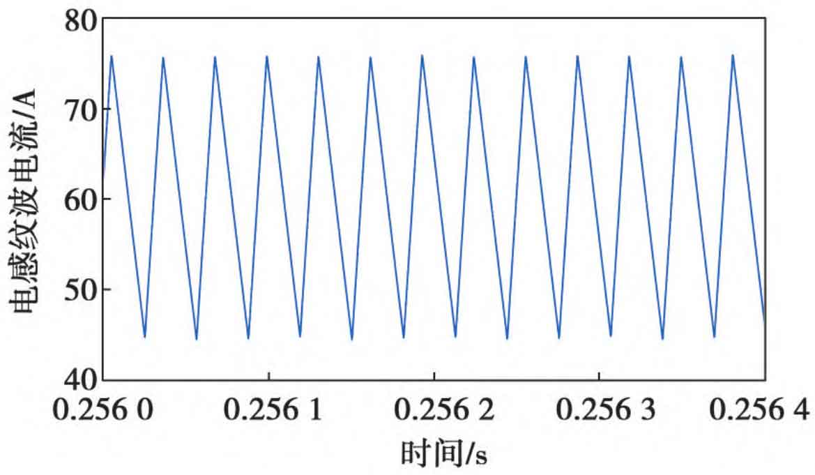
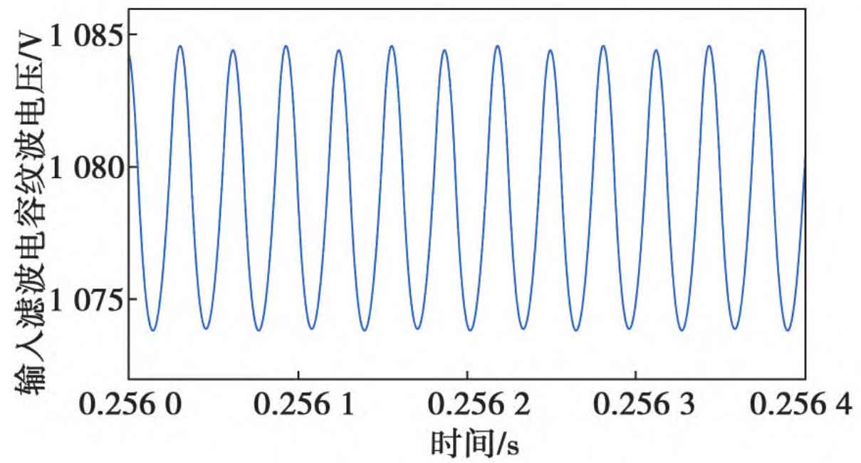
Select a certain string of photovoltaic inverters for design, and calculate the parameters of the flyover Boost main circuit through Chapter 2, as shown in the first column of Table 4; According to the dynamic control strategy, under the input voltage of 1080 V and the output DC bus voltage of 1300 V, the simulation results of the ripple current/voltage of the main circuit components are shown in the third column of Table 4, and the simulation waveforms are shown in Figures 8 to 10.
| Main circuit parameters | Calculation value of main circuit parameters | Ripple current/ripple voltage peak to peak limit | Simulation results of ripple current/ripple voltage peak to peak value |
| Input filtering inductance | 150 μH | 36 A | 31.40 A |
| Input filtering capacitor | 14 μF | 20 V | 11.17 V |
| Flying capacitor | 42 μF | 65 V | 16.14 V |
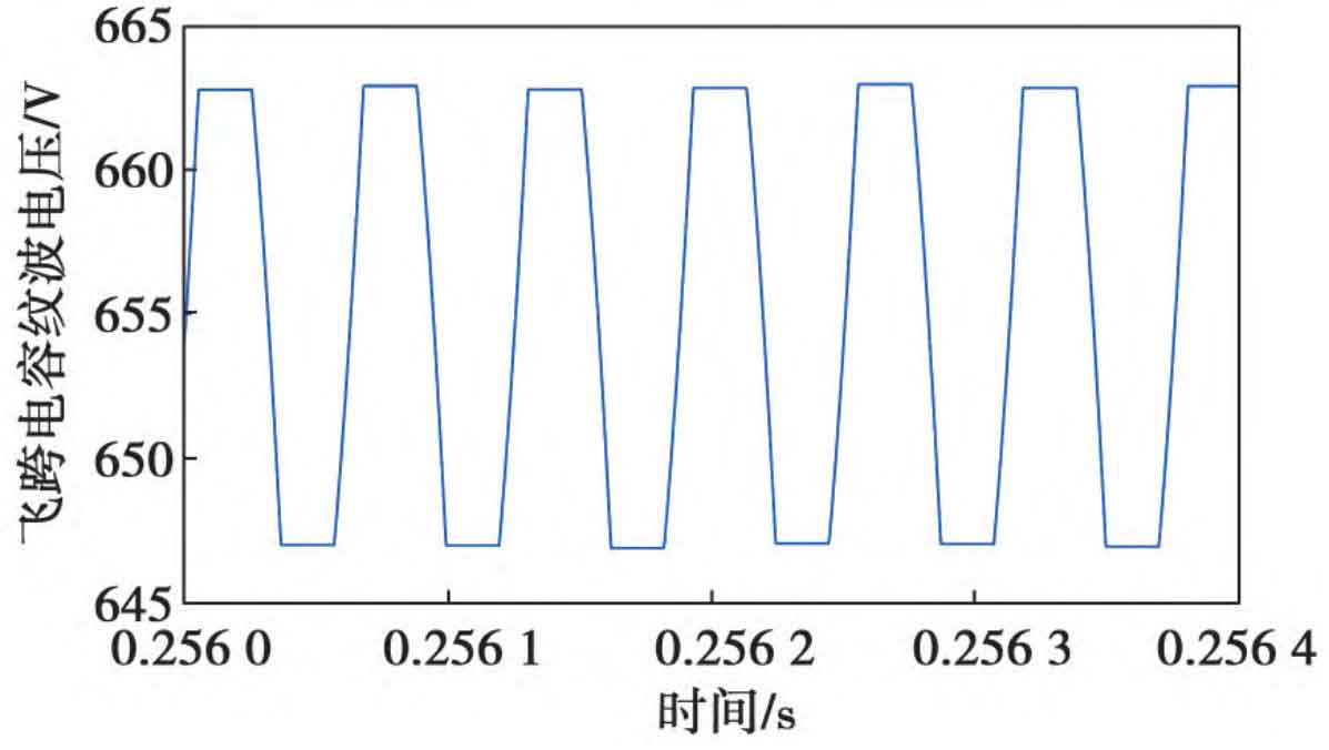
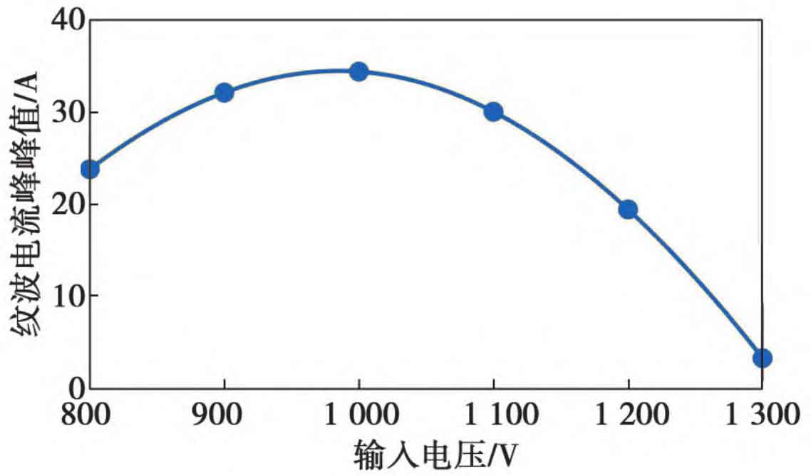
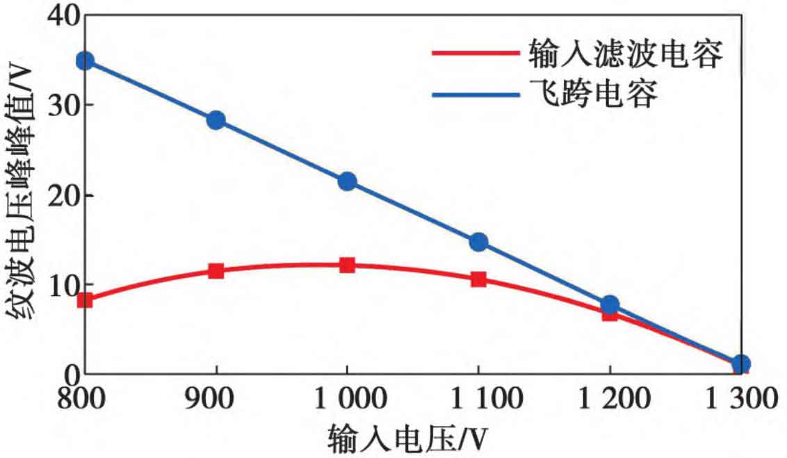
According to the simulation results, it can be seen that the actual peak to peak values of the inductor ripple current and capacitor ripple voltage in the flyover Boost circuit are both less than the limit values, and the average inductor current is stable at 60 A, while the average voltage of the flyover capacitor is stable at 655 V. This verifies the effectiveness of the main circuit parameters and control strategy. To observe the operation of the Flyover Boost circuit under the constantly changing output voltage of the front-end photovoltaic panel, the following adjustments are made: keep the input current and output DC bus voltage unchanged, and change the input voltage. The peak to peak changes of inductor ripple current, input filtering capacitor ripple voltage, and flying capacitor ripple voltage are shown in Figures 11 and 12. From Figures 11 and 12, it can be seen that the peak to peak value of the inductor ripple current first increases and then decreases with the increase of input voltage. The trend of the peak to peak value of the input filtering capacitor ripple voltage is the same, while the peak to peak value of the flying capacitor ripple voltage decreases with the increase of input voltage, but all three change within the expected design limit.
5. Conclusion
This article analyzes and studies the working principle, power switch device selection, and main circuit parameter design method of a flying capacitor three-level Boost circuit. Based on engineering examples, a series photovoltaic inverter front-end DC/DC boost main circuit was designed, and the parameters of each power switch device were calculated. The simulation results show that under the dynamic control strategy, the control of inductor current and flying capacitor voltage is stable, and the input filtering inductor ripple current, input filtering capacitor ripple voltage, and flying capacitor ripple voltage all vary within the expected design limits. This verifies the effectiveness of the main circuit design and provides a DC/DC boost solution for high power density and high voltage level string photovoltaic inverters.