
1. Introduction and Research Background
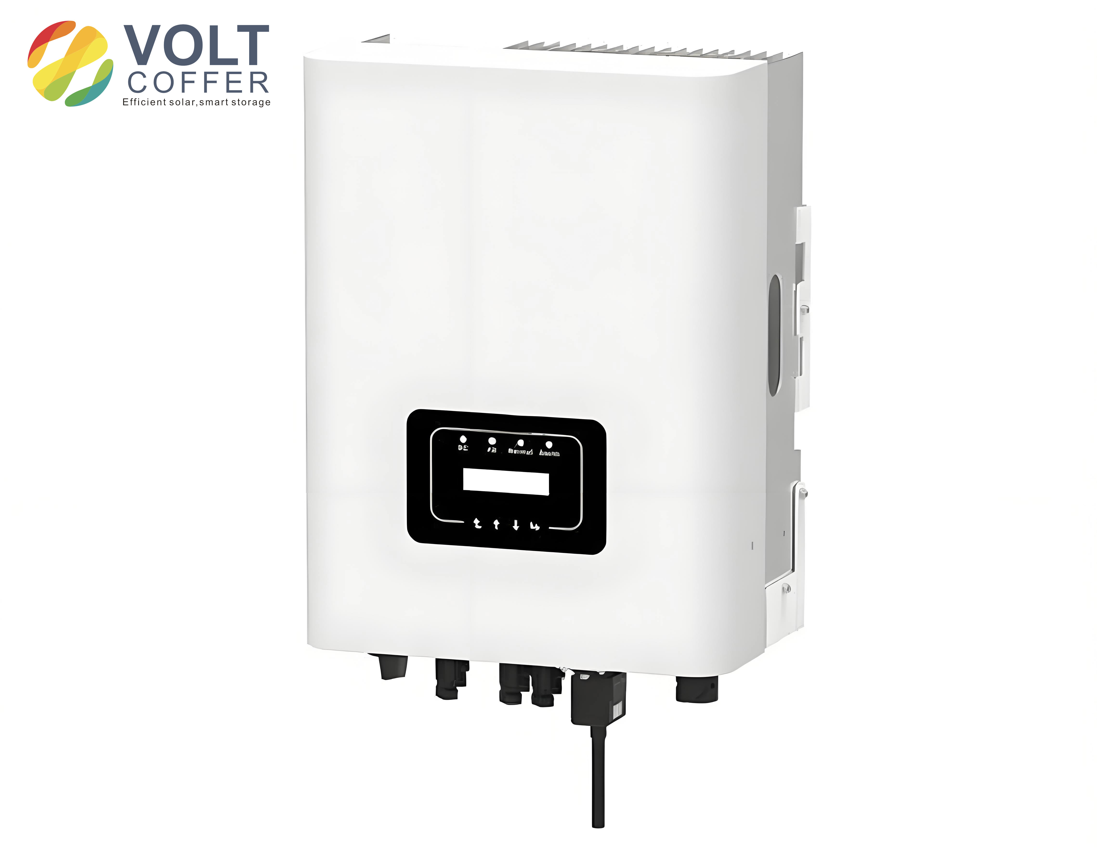
The increasing global demand for renewable energy has accelerated the development of photovoltaic power generation systems. Among various renewable energy sources, solar energy has emerged as one of the most promising alternatives due to its abundance, cleanliness, and wide distribution. In my research, I focus on grid-connected photovoltaic systems, where the inverter plays a crucial role in converting DC power from photovoltaic panels into AC power suitable for grid integration. The inverter topologies can be broadly classified into isolated and non-isolated types. Isolated inverters incorporate transformers to provide electrical isolation, while non-isolated inverters, also known as transformerless inverters, directly connect the photovoltaic array to the grid without galvanic isolation.
Non-isolated solar inverters have gained significant attention in recent years because of their relatively small size, low cost, and high conversion efficiency. However, the absence of transformer isolation introduces a critical problem: the leakage current. The photovoltaic array inherently has parasitic capacitance to the ground. In transformerless systems, this parasitic capacitance forms a closed loop with the inverter, the filter components, and the grid. When the common-mode voltage changes at high frequency, a current flows through this parasitic capacitance, which is referred to as leakage current. This leakage current poses serious threats to both equipment safety and personal safety. The magnitude and frequency of the leakage current must be strictly limited according to international standards. For instance, the VDE-0126-1-1 standard mandates that the grid should be disconnected within 0.3s if the leakage current exceeds 300mA. Therefore, my research is dedicated to investigating modulation techniques that can effectively suppress leakage current in transformerless three-phase solar inverters.
2. Generation Mechanism of Leakage Current in Solar Inverters
To better understand the leakage current issue, I established a common-mode equivalent circuit model for the transformerless system. The leakage current path is formed by the photovoltaic parasitic capacitance, the inverter switches, the filter components, and the grid impedance. The common-mode voltage is defined as the average of the output voltages of all bridge legs. For a general four-leg inverter, the common-mode voltage \( V_{CM} \) can be expressed as:
\[
V_{CM} = \frac{V_{AN} + V_{BN} + V_{CN} + V_{DN}}{4}
\]
where \( V_{AN} \), \( V_{BN} \), \( V_{CN} \), and \( V_{DN} \) are the output voltages of the four legs with respect to the negative DC bus. I analyzed the circuit in the frequency domain. The voltage across the parasitic capacitance \( V_{PV} \) is related to the common-mode voltage and the fourth-leg capacitor voltage \( V_{Cf4} \) as follows:
\[
V_{PV}(s) = a(s)V_{CM}(s) + bV_{Cf4}(s)
\]
where \( a(s) \) and \( b \) are coefficients that depend on the filter parameters and parasitic capacitance. The leakage current \( i_k \) is then obtained by:
\[
i_k = -C_{PV}\frac{dv_{PV}(t)}{dt}
\]
From the equations above, I concluded that the key to suppressing leakage current is to maintain the common-mode voltage constant. If the common-mode voltage remains stable without high-frequency components, the voltage across the parasitic capacitance will also be stable, thus minimizing the leakage current.
3. Research on Modulation Techniques for Two-Level Three-Phase Four-Leg Solar Inverters
3.1 Working Principle and Common-Mode Characteristics
My research begins with the two-level three-phase four-leg inverter, as shown in the topology I studied. It consists of eight switches forming four bridge legs. Each leg has two working states. State “1” means the upper switch is turned on, and the output voltage of that leg is \( V_{dc} \). State “0” means the lower switch is turned on, and the output voltage is 0. Therefore, there are a total of \( 2^4 = 16 \) switching states. I analyzed the common-mode voltage for each state, and the results are summarized in the table below.
Table 1: Output voltages and common-mode voltages of the two-level four-leg inverter
| Common-mode voltage | Working states |
|---|---|
| \( V_{dc} \) | 1111 |
| \( 3V_{dc}/4 \) | 1110, 1101, 1011, 0111 |
| \( V_{dc}/2 \) | 1100, 1001, 0011, 0101, 1010, 0110 |
| \( V_{dc}/4 \) | 0001, 0010, 0100, 1000 |
| 0 | 0000 |
3.2 Analysis of Existing Space Vector Modulation Techniques
I first examined the traditional space vector pulse width modulation (SVPWM) method for the two-level three-phase four-leg inverter. In a switching period, the traditional SVPWM generates eight switching actions. The common-mode voltage frequently changes among five levels: \( V_{dc} \), \( 3V_{dc}/4 \), \( V_{dc}/2 \), \( V_{dc}/4 \), and 0. This high-frequency fluctuation of the common-mode voltage results in a large leakage current. My simulations showed that the peak leakage current reaches 1.08A, which far exceeds the standard limit.
In the modified space vector pulse width modulation (MSVPWM), the zero vectors are replaced by a pair of complementary active vectors. This method reduces the switching actions to increase the number of switching actions from 8 to 12. The variation range of the common-mode voltage is reduced to \( V_{dc}/4 – 3V_{dc}/4 \). The peak leakage current is reduced to 0.85A. However, it is still far beyond the standard requirement.
For the remote-state space vector pulse width modulation (RSVPWM), only vectors with the same common-mode voltage are utilized. This method can maintain the common-mode voltage constant at \( V_{dc}/2 \). However, it has a limited DC voltage utilization rate, with the maximum modulation index being only 1, and it introduces additional switching losses with 12 switching actions per period. The leakage current peak value is 23mA.
3.3 Analysis of Existing Carrier-Based Modulation Techniques
The carrier modulation technique with Boolean logic functions (BLCM) was also investigated. It uses an XOR logic gate for the fourth leg. This strategy can effectively suppress leakage current because the common-mode voltage stays at \( V_{dc}/2 \). However, it has the disadvantage of a low DC utilization rate, and the number of switching actions varies between 8, 12, and 14 times per switching period, depending on the sector.
3.4 Proposed Improved Carrier Modulation (ICM)
In order to solve the aforementioned problems, I proposed an improved carrier modulation (ICM) strategy for the two-level three-phase four-leg solar inverter. The key idea is to flexibly choose different carrier waveforms in different sectors to achieve a constant common-mode voltage while also improving other performance parameters. I used three types of carrier waveforms: a downward sawtooth carrier \( V_{tri1} \), an upward sawtooth carrier \( V_{tri2} \), and a symmetrically centered triangular carrier \( V_{tri3} \). The control block diagram consists of adding a zero-sequence component \( V_e \) to the three-phase sinusoidal reference voltages. The zero-sequence component is calculated as:
\[
V_e = -\frac{V_{max} + V_{min}}{2}
\]
where \( V_{max} = max(V_{ma}, V_{mb}, V_{mc}) \) and \( V_{min} = min(V_{ma}, V_{mb}, V_{mc}) \). With this injection, the phase voltages can be expressed as:
\[
V_{max}^* = V_{max} – \frac{V_{max} + V_{min}}{2} = \frac{V_{max} – V_{min}}{2}
\]
\[
V_{mid}^* = V_{mid} – \frac{V_{max} + V_{min}}{2}
\]
\[
V_{min}^* = -V_{max}^*
\]
The maximum modulation index is increased to 1.15. I then compared the maximum phase voltage \( V_{max}^* \) and the minimum phase voltage \( V_{min}^* \) with the downward and upward sawtooth carriers, while the intermediate phase \( V_{mid}^* \) was compared with the symmetric triangular carrier. The fourth bridge leg control signal \( S_7 \) is obtained via the XOR gate:
\[
S_7 = S_1 \oplus S_3 \oplus S_5
\]
The sectors are identified based on the relative magnitude of the three-phase voltages. The carrier allocation for different sectors is given in the table below.
Table 2: Carrier selection for the ICM method (Combination 1)
| Carrier | Sector I | Sector II | Sector III | Sector IV | Sector V | Sector VI |
|---|---|---|---|---|---|---|
| \( V_{triA} \) | \( V_{tri1} \) | \( V_{tri3} \) | \( V_{tri2} \) | \( V_{tri2} \) | \( V_{tri3} \) | \( V_{tri1} \) |
| \( V_{triB} \) | \( V_{tri3} \) | \( V_{tri1} \) | \( V_{tri1} \) | \( V_{tri3} \) | \( V_{tri2} \) | \( V_{tri2} \) |
| \( V_{triC} \) | \( V_{tri2} \) | \( V_{tri2} \) | \( V_{tri3} \) | \( V_{tri1} \) | \( V_{tri1} \) | \( V_{tri3} \) |
With this carrier allocation, the zero vectors are eliminated, and only the states with a common-mode voltage of \( V_{dc}/2 \) are used. Consequently, the common-mode voltage remains constant, and the leakage current is effectively suppressed. In the ICM method, the total number of switching actions in one period is eight, which is the same as the traditional SVPWM. This means that my proposed method does not introduce additional switching losses while achieving leakage current suppression. Moreover, the DC voltage utilization rate is as high as 1.15.
3.5 Simulation and Experimental Verification of ICM
I conducted extensive simulations to evaluate the performance of the ICM strategy. The simulation parameters were: DC voltage 120V, switching frequency 15kHz, modulation index 0.9, parasitic capacitance 300nF, filter inductance 5mH, and filter capacitance 10μF. The simulation results showed that the common-mode voltage was kept constant at 60V. The peak leakage current was 29mA, and the RMS leakage current was 11.4mA, both well below the standard VDE-0126-1-1 limits. I also built a two-level four-leg inverter experimental platform. The ICM modulation was implemented on a FPGA-based controller. The experimental results closely match the simulations. The leakage current RMS value measured was 26.5mA, which is lower compared to other methods. I also observed the output phase voltage waveforms. In the ICM method, the fourth leg voltage changes only twice per switching period, whereas in the MSVPWM and RSVPWM methods, it changes six times. This confirms the lower switching loss characteristic of the ICM method. The comparison of the five modulation strategies for the two-level inverter is shown in the following table.
Table 3: Performance comparison of modulation strategies for two-level inverters
| Modulation Strategy | Peak leakage current (mA) | RMS leakage current (mA) | Common-mode voltage (V) | Switching actions per period | Modulation index range |
|---|---|---|---|---|---|
| SVPWM | 1080 | 671 | 0-120 | 8 | 0-1.15 |
| MSVPWM | 850 | 472 | 30-90 | 12 | 0-1.15 |
| RSVPWM | 23 | 10.2 | 60 | 12 | 0-1 |
| BLCM | 17 | 6.6 | 60 | 8/12/14 | 0-1 |
| ICM | 29 | 11.4 | 60 | 8 | 0-1.15 |
4. Research on Modulation Techniques for Three-Level Three-Phase Four-Leg Solar Inverters
4.1 Working Principle and Common-Mode Characteristics
After completing the two-level inverter study, I extended my research to the three-level three-phase four-leg solar inverter, specifically the diode-clamped topology. In this topology, each bridge leg has three working states: state “2” (output voltage \( V_{dc} \)), state “1” (output voltage \( V_{dc}/2 \)), and state “0” (output voltage 0). Therefore, the output voltage of each phase can be expressed as:
\[
V_{xN} = \frac{V_{dc}}{2} S_x \quad (x = A, B, C, D)
\]
where \( S_x \in \{0, 1, 2\} \) is the switching state of the leg. With four legs, there are \( 3^4 = 81 \) switching states. The common-mode voltage is calculated by:
\[
V_{CM} = \frac{V_{dc}}{8} (S_A + S_B + S_C + S_D)
\]
To keep the common-mode voltage constant at \( V_{dc}/2 \), the sum of the switching states must equal 4:
\[
S_A + S_B + S_C + S_D = 4
\]
I identified that there are 19 switching states that satisfy this condition and produce a constant common-mode voltage. These are listed in Table 4. The other states are categorized as invalid vectors.
Table 4: Valid switching states for constant common-mode voltage in three-level four-leg inverter
| Vector type | Working states | Common-mode voltage |
|---|---|---|
| Large vectors | 0220, 2200, 2002, 2020, 0022, 0220 | \( V_{dc}/2 \) |
| Medium vectors | 1201, 2101, 2011, 1021, 0120, 0211 | \( V_{dc}/2 \) |
| Small vectors | 1210, 1102, 2110, 1012, 1120, 0112 | \( V_{dc}/2 \) |
| Zero vector | 1111 | \( V_{dc}/2 \) |
4.2 Traditional and Existing Modulation Strategies
I analyzed two traditional carrier modulation strategies: in-phase disposition modulation (IPDM) and opposite-phase disposition modulation (OPDM). In the IPDM method, the common-mode voltage fluctuates among five levels: \( 3V_{dc}/8 \), \( V_{dc}/2 \), \( 5V_{dc}/8 \), \( 3V_{dc}/4 \), and \( 7V_{dc}/8 \). The peak-to-peak fluctuation is \( V_{dc}/2 \), which produces a leakage current with an RMS value of 328mA. This is not acceptable.
For the OPDM method, the two triangular carriers are 180 degrees out of phase. The common-mode voltage has four levels: \( 3V_{dc}/8 \), \( V_{dc}/2 \), \( 5V_{dc}/8 \), and \( 3V_{dc}/4 \). The RMS leakage current is 150mA. While this is lower than the IPDM, it still does not meet the standard requirements.
I also studied an existing leakage current suppression method called MOPDM. In this method, the fourth leg switching state is determined by:
\[
S_D = 4 – S_A – S_B – S_C
\]
This method maintains the common-mode voltage constant and effectively suppresses the leakage current. However, it requires 12 switching actions per period, which increases the switching losses.
4.3 Proposed Sawtooth Combination Modulation (SCM)
To overcome the disadvantages of the existing methods, I proposed a sawtooth combination modulation (SCM) strategy. This method shares the same philosophy as the ICM: utilizing different carrier shapes to optimize system performance without changing the output duty cycles. In the SCM method, I use an upward sawtooth carrier \( V_{tri2} \) and a downward sawtooth carrier \( V_{tri1} \). Two schemes are possible. In Scheme 1, the upper carrier \( V_{trix} \) is \( V_{tri2} \), and the lower carrier \( V_{triy} \) is \( V_{tri1} \). In Scheme 2, the upper carrier is \( V_{tri1} \) and the lower carrier is \( V_{tri2} \). The modulation signals are obtained by adding the third harmonic to the three-phase reference:
\[
V_{ma}^* = V_{ma} + V_e
\]
\[
V_{mb}^* = V_{mb} + V_e
\]
\[
V_{mc}^* = V_{mc} + V_e
\]
where \( V_e = \frac{1}{6}\sin(3\omega t) \). The fourth leg state is calculated from:
\[
S_D = 4 – S_A – S_B – S_C
\]
The SCM method filters out the invalid states and only allows the 19 states with constant common-mode voltage. As a result, the common-mode voltage remains constant at \( V_{dc}/2 \). The DC voltage utilization is high with a maximum modulation index of 1.15. In one switching period, the first three legs each switch twice, while the fourth leg switches four times. Thus, the total number of switching actions is 10, which is fewer than the 12 actions in the MOPDM method. This leads to lower switching losses.
5. Neutral Point Potential Balance Control for Solar Inverters
5.1 Problem Statement
The diode-clamped three-level four-leg inverter suffers from the neutral point potential imbalance issue, which is an inherent problem. The neutral point potential deviation is caused by the unequal charging and discharging of the DC-link capacitors. The midpoint current flows through the neutral point when any bridge leg is in state “1”. The relationship between the neutral point voltage \( V_o \) and the midpoint current \( i_o \) is:
\[
\frac{dV_o}{dt} = -\frac{i_o}{2C_{dc}}
\]
where \( C_{dc} \) is the DC-link capacitance. This unbalanced potential has several adverse effects, including distorted output voltages and increased harmonic content. More importantly, in the context of my research, I discovered that the neutral point potential fluctuation also affects the leakage current. Since the common-mode voltage includes the voltage levels of the bridge legs connected to the neutral point, any fluctuation in the neutral point potential directly causes the common-mode voltage to deviate from its constant value. This degrades the leakage current suppression effectiveness. Therefore, maintaining the neutral point potential balance is crucial for both the output power quality and the leakage current suppression.
5.2 Proposed Neutral Point Potential Balance Control
I proposed a neutral point potential balance control strategy embedded in the SCM method. The control diagram is based on the feedback of the DC capacitor voltage difference \( \Delta U_C = U_{C1} – U_{C2} \). The required average midpoint current \( i_{np0} \) is calculated as:
\[
i_{np0} = \frac{C_{dc} \Delta U_C}{T_s}
\]
where \( T_s \) is the switching period. A zero-sequence voltage \( V_0 \) is then injected into the modulation signals. This zero-sequence component is derived from the principle that the average current flowing into the neutral point should be zero. I derived the zero-sequence expression based on the sector and the polarity of the intermediate modulation signal. The general expression for the zero-sequence component is:
\[
V_0 =
\begin{cases}
-\frac{V_{max}^*(i_{max} – i_{mid}) + V_{mid}^*(i_{max} – i_{min}) + i_{np0}}{2(i_{max} – i_{mid})}, & V_{mid}^* \geq 0 \\
\frac{V_{mid}^*(i_{max} – i_{min}) + V_{min}^*(i_{mid} – i_{max}) + i_{np0}}{2(i_{mid} – i_{min})}, & V_{mid}^* < 0
\end{cases}
\]
where \( i_{max} \), \( i_{mid} \), and \( i_{min} \) are the currents corresponding to the maximum, intermediate, and minimum phase modulation signals, respectively. The zero-sequence component must satisfy the constraint:
\[
-1 – V_{min} \leq V_0 \leq 1 – V_{max}
\]
By injecting this zero-sequence component, the average midpoint current is forced to zero, thus maintaining the neutral point potential balance.
5.3 Simulation and Experimental Results for SCM and Neutral Point Control
I conducted simulations for the three-level four-leg inverter with the SCM method and the proposed neutral point potential balance control. The DC bus voltage was set to 120V, and the two DC capacitors were selected as 100μF and 68μF in separate tests. In the case of 100μF capacitors, before adding the neutral point potential balance control, the capacitor voltage fluctuation was about 10V. After the control was enabled, the fluctuation was reduced to only 0.6V, and both capacitor voltages were well balanced at around 60V. In the case of 68μF capacitors, the fluctuation was reduced from 16V to 0.8V.
I also observed the impact of neutral point potential balance on leakage current. For the 100μF capacitors, the leakage current RMS value was 17.53mA before control and 6.76mA after control. For the 68μF capacitors, the RMS value was 24.42mA before control and 6.69mA after control. These results confirm that the neutral point potential balance control effectively suppresses the leakage current in solar inverters.
I built a three-level four-leg inverter experimental platform to verify my proposed methods. The experimental results for the leakage current are summarized in the table below.
Table 5: Leakage current RMS values under different modulation strategies for the three-level four-leg solar inverter
| Modulation Strategy | RMS leakage current (mA) | Switching actions per period |
|---|---|---|
| IPDM | 560 | 8 |
| OPDM | 87.7 | 8 |
| MOPDM | 26.6 | 12 |
| SCM | 27.7 | 10 |
The experimental waveforms further confirmed that the SCM method maintains the parasitic capacitor voltage almost constant with only a small third-harmonic ripple. The output phase voltages show that the SCM method achieves a good balance between switching losses and leakage current suppression. The neutral point potential balance control was also tested experimentally. The results showed that the capacitor voltages were well balanced with a negligible fluctuation. The leakage current was further reduced after enabling the neutral point potential balance control, demonstrating the effectiveness of my proposed control strategy.
6. Conclusion
In my research, I have systematically investigated the leakage current suppression problem in transformerless three-phase solar inverters. For the two-level three-phase four-leg inverter, I proposed an improved carrier modulation strategy that flexibly selects different carrier waveforms in different sectors. This method maintains the common-mode voltage constant, effectively suppresses the leakage current, does not increase switching losses, and achieves a high DC voltage utilization rate. For the three-level three-phase four-leg inverter, I proposed a sawtooth combination modulation strategy that uses upward and downward sawtooth carriers. This method also maintains a constant common-mode voltage with lower switching losses compared to existing methods. Furthermore, I addressed the neutral point potential imbalance problem by proposing a zero-sequence injection method based on the SCM strategy. This method effectively balances the neutral point potential and further improves the leakage current suppression performance. Both simulation and experimental results have validated the correctness and effectiveness of my proposed methods. The findings of my research contribute to the safe and reliable operation of transformerless solar inverters.