
In recent years, the growing energy crisis and environmental pollution have significantly impacted human survival, driving the rapid development of renewable energy systems such as photovoltaic (PV) power generation. Solar energy, with its abundant reserves and ease of installation, is regarded as a primary direction for future energy sources. In PV systems, the grid-connected solar inverter plays a crucial role as the core device. Traditional topologies often employ two-level inverters, but these suffer from drawbacks like high output current harmonics, necessitating large filter inductors. To overcome these limitations, three-level inverters have been proposed, offering advantages such as lower harmonics and reduced electromagnetic interference. Consequently, three-level structures have become an important choice in PV power generation systems. To meet high-voltage requirements in PV systems, numerous PV panels need to be connected in series, leading to so-called single-stage inverters. However, this configuration can result in low maximum power point tracking (MPPT) efficiency. Therefore, a DC/DC converter is added at the front end of the inverter, forming a two-stage solar inverter topology. Compared to single-stage systems, two-stage solar inverters provide higher MPPT efficiency and require fewer series-connected panels.
Non-isolated PV solar inverters face the issue of leakage current, which, if not suppressed, can cause distortion in grid-connected currents. National standards mandate that for solar inverters below 30 kW, leakage current must be kept below 300 mA. In this context, I propose a two-stage single-phase three-level grid-connected solar inverter topology, where the DC/DC capacitor midpoint is connected to the three-level inverter capacitor midpoint. This approach effectively suppresses leakage current and ensures high-quality grid-connected current. Compared to traditional methods, this topology not only mitigates leakage current but also enables midpoint balance control. The rear-stage inverter utilizes a deadbeat control strategy combined with space vector modulation to achieve grid current control. The advantages of this method include effective leakage current suppression, robust grid connection even at high modulation indices, and faster dynamic response compared to PI-based control methods. The correctness of the proposed algorithm is verified through simulation and experimental results.
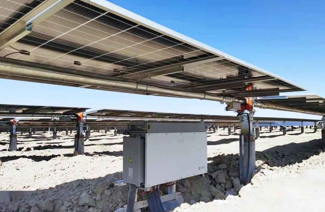
The proposed solar inverter system consists of a three-level DC/DC converter followed by a single-phase three-level inverter. The DC/DC stage is responsible for boosting the PV voltage and maintaining midpoint balance, while the inverter stage handles grid connection. To analyze the DC/DC three-level converter simply, assume steady-state conditions where the DC-side voltages \(U_{dc1}\) and \(U_{dc2}\) are equal, each at \(U_{dc}/2\). The voltage \(U_{S1}\) over one switching period \(T_s\) is defined as:
$$U_{S1}(t) = \begin{cases} 0 & \text{if } S_{1P} = 1 \\ \frac{U_{dc}}{2} & \text{if } S_{1P} = 0 \end{cases}$$
Applying Kirchhoff’s law, the voltage equation for \(U_{S1}\) over one period is:
$$L_1 \frac{di_{L1}}{dt} = U_{C1} – U_{S1}$$
This can be equivalently expressed as:
$$0 = \int_0^{T_s} (U_{C1} – U_{S1}) dt$$
Thus, the capacitor voltage \(U_{C1}\) over one period \(T_s\) is:
$$U_{C1} = \frac{1}{T_s} \int_0^{T_s} U_{S1} dt$$
Substituting the duty cycle \(D\):
$$U_{C1} = \frac{1}{T_s} \int_{DT_s}^{T_s} \frac{U_{dc}}{2} dt = \frac{U_{dc}}{2} (1 – D)$$
The voltages across capacitors \(U_{C1}\) and \(U_{C2}\) are:
$$U_{C1} = U_{C2} = \frac{U_{PV}}{2}$$
Therefore, the duty cycle for the DC/DC controller is:
$$D = 1 – \frac{U_{PV}}{U_{dc}}$$
Additionally, the balance duty cycle adjustment is given by:
$$\Delta d = K_{p,\text{balance}} (U_{dc1} – U_{dc2})$$
From this equation, it is evident that by tuning \(K_{p,\text{balance}}\), midpoint potential balance control can be achieved. The control algorithm for the three-level DC/DC midpoint balance is summarized in the following table:
| Control Component | Function | Equation |
|---|---|---|
| DC/DC Duty Cycle | Regulate PV voltage boost | \(D = 1 – \frac{U_{PV}}{U_{dc}}\) |
| Balance Adjustment | Maintain midpoint voltage balance | \(\Delta d = K_p (U_{dc1} – U_{dc2})\) |
| Leakage Current Suppression | Reduce parasitic capacitance effects | Based on topology connection |
The equivalent circuits of traditional and proposed solar inverter topologies highlight the leakage current suppression mechanism. In the proposed system, the parasitic capacitor voltage \(U_{PV}\) is decoupled from the inverter output voltage \(U_{an}\), and high-frequency components in \(U_{bn}\) are filtered by inductor \(L_2\). This significantly reduces system leakage current.
For the single-phase NPC-type three-level inverter, the grid voltage, line current, and input voltage can be expressed in terms of d-q components as:
$$\begin{cases} u_s = u_d \cos(\omega t) + u_q \sin(\omega t) \\ i_s = i_d \cos(\omega t) + i_q \sin(\omega t) \\ u_{ab} = u_{abd} \cos(\omega t) + u_{abq} \sin(\omega t) \end{cases}$$
where \(\omega\) is the grid frequency, and \(u_d\), \(u_q\), \(i_d\), \(i_q\), \(u_{abd}\), \(u_{abq}\) are the d-q axis components of grid voltage, current, and input voltage, respectively. The cosine and sine components of \(u_s\) are derived as:
$$u_s \cos(\omega t) = \frac{u_d}{2} + \frac{u_d \cos(2\omega t) + u_q \sin(2\omega t)}{2}$$
$$u_s \sin(\omega t) = \frac{u_q}{2} + \frac{u_d \sin(2\omega t) + u_q \cos(2\omega t)}{2}$$
Based on Kirchhoff’s law, the mathematical model of the three-level inverter is:
$$L \frac{di_s}{dt} = -u_s – R i_s + u_{ab}$$
Thus, the d-q axis expressions for \(u_{ab}\) are:
$$\begin{cases} u_{abd} = u_d – R i_d – L \frac{di_d}{dt} – \omega L i_q \\ u_{abq} = u_q – R i_q – L \frac{di_q}{dt} + \omega L i_d \end{cases}$$
Discretizing these equations with sampling period \(T_s\) yields:
$$\begin{cases} u_{abd}(k) = u_d(k) – R i_d(k) – L \frac{i_d(k+1) – i_d(k)}{T_s} – \omega L i_q(k) \\ u_{abq}(k) = u_q(k) – R i_q(k) – L \frac{i_q(k+1) – i_q(k)}{T_s} + \omega L i_d(k) \end{cases}$$
To account for control delays, the equations are advanced by one step:
$$\begin{cases} u_{abd}(k+1) = u_d(k+1) – R i_d(k+1) – L \frac{i_d(k+2) – i_d(k+1)}{T_s} – \omega L i_q(k+1) \\ u_{abq}(k+1) = u_q(k+1) – R i_q(k+1) – L \frac{i_q(k+2) – i_q(k+1)}{T_s} + \omega L i_d(k+1) \end{cases}$$
Transforming back to the stationary coordinate system gives the voltages for space vector modulation:
$$\begin{bmatrix} u_{ab\alpha}(k+1) \\ u_{ab\beta}(k+1) \end{bmatrix} = \begin{bmatrix} \cos(\omega t) & \sin(\omega t) \\ \sin(\omega t) & -\cos(\omega t) \end{bmatrix} \begin{bmatrix} u_{abd}(k+1) \\ u_{abq}(k+1) \end{bmatrix}$$
where \(u_{ab\alpha}\) and \(u_{ab\beta}\) are inputs to the space vector modulator. Assuming the O point of the single-phase three-level inverter as reference, each phase output voltage can be \(U_{dc}/2\), 0, or \(-U_{dc}/2\), corresponding to P, O, N states. The space vector modulation for the single-phase three-level solar inverter includes nine vectors: large, medium, small, and zero vectors. The switching states and voltage vectors are summarized in the following table:
| Vector Type | Switching States (P-type) | Switching States (N-type) |
|---|---|---|
| Zero Vectors | [PP], [OO], [NN] | – |
| Small Vectors | [PO], [OP] | [ON], [NO] |
| Large Vectors | [PN] | [NP] |
The reference voltage vector is represented as:
$$U_{\text{ref}} = u_{ab\alpha} + j u_{ab\beta}$$
Using the nearest three vectors, the duty times are calculated as:
$$\begin{cases} U_{\text{ref}} T = U_a T_a + U_b T_b + U_0 T_0 \\ T = T_a + T_b + T_0 \end{cases}$$
where \(T_0\) is the zero vector duration, \(U_0\) is the zero vector, \(U_a\) and \(U_b\) are non-zero vectors, and \(T_a\) and \(T_b\) are their respective durations. This modulation strategy minimizes switching frequency and improves efficiency in the solar inverter.
To validate the proposed two-stage single-phase three-level solar inverter topology and control algorithm, a simulation model of a 10 kW system was developed. Key parameters include: grid voltage \(e_a = 220 \, \text{V}\), DC-side voltage \(U_{dc} = 400 \, \text{V}\), DC-side capacitors \(C_{dc1} = C_{dc2} = 3300 \, \mu\text{F}\), reference currents \(i_d^* = 50/20/15 \, \text{A}\), grid-side filter inductance \(L = 3 \, \text{mH}\), grid frequency \(50 \, \text{Hz}\), DC-link capacitors \(C_1 = C_2 = 6.6 \, \mu\text{F}\), and DC-side inductance \(L_1 = 0.25 \, \text{mH}\). The system comprises the DC/DC converter, single-phase three-level inverter, filter, and grid.
Simulation results demonstrate the effectiveness of the proposed method. Leakage current waveforms comparing traditional and proposed approaches show significant suppression with the new topology. The line-to-line voltage waveforms of the single-phase three-level inverter exhibit good quality under the proposed control. In scenarios with initially unequal capacitor voltages, the proposed method achieves voltage balance control more rapidly than traditional techniques. Additionally, step changes in reference current from 15 A to 20 A highlight the faster tracking capability of the deadbeat control compared to PI control.
Experimental verification was conducted with parameters: grid voltage \(e_a = 220 \, \text{V}\), DC-side voltage \(U_{dc} = 400 \, \text{V}\), DC-side capacitors \(C_{dc1} = C_{dc2} = 3300 \, \mu\text{F}\), reference currents \(i_d^* = 22/15 \, \text{A}\), grid-side filter inductance \(L = 3 \, \text{mH}\), grid frequency \(50 \, \text{Hz}\), DC-link capacitors \(C_1 = C_2 = 6.6 \, \mu\text{F}\), and DC-side inductance \(L_1 = 0.25 \, \text{mH}\). Experimental waveforms of line-to-line voltage confirm good performance. Step responses in reference current from 8 A to 22 A show that the proposed method provides quicker tracking compared to traditional PI control, validating the dynamic response advantages of the deadbeat strategy in solar inverter applications.
In conclusion, the proposed two-stage single-phase three-level grid-connected solar inverter topology effectively addresses leakage current and midpoint balance issues. The DC/DC stage ensures midpoint potential balance and suppresses leakage current, while the rear-stage inverter employs deadbeat control and space vector modulation for efficient grid connection. Compared to conventional methods, this solar inverter system offers several benefits: substantial reduction in leakage current meeting grid standards, rapid midpoint balance control via deadbeat techniques, elimination of complex PI tuning, and robust performance even at high modulation indices. Therefore, this topology and control strategy are highly suitable for widespread application in PV grid-connected power generation systems. The integration of advanced modulation and control methods enhances the reliability and efficiency of solar inverters, contributing to the broader adoption of renewable energy.
Further research could explore scalability to higher power levels or integration with energy storage systems. The principles discussed here provide a foundation for optimizing solar inverter designs in future smart grids. As the demand for clean energy grows, innovations in solar inverter technology will continue to play a pivotal role in achieving sustainable power systems.