
As a researcher focused on renewable energy technologies, I have dedicated my efforts to advancing thin film solar panels, particularly those based on copper indium gallium selenide (CIGS) absorbers. Thin film solar panels offer a promising path toward low-cost, high-efficiency photovoltaic devices, and among them, CIGS-based panels have emerged as a leading contender due to their superior performance and stability. In this article, I will delve into the critical role of the back electrode in CIGS thin film solar panels, detailing my experimental work on molybdenum (Mo) as the back contact material. The back electrode serves as the foundation for the entire solar cell structure, influencing electrical conductivity, adhesion, and overall efficiency. Through meticulous preparation and characterization, I aim to elucidate the optimal conditions for Mo deposition and its impact on device performance, with a focus on enhancing the viability of thin film solar panels for widespread adoption.
The global energy landscape is rapidly evolving, driven by the urgent need to transition from fossil fuels to sustainable sources. Thin film solar panels represent a key technology in this shift, offering advantages such as flexibility, lightweight design, and reduced material usage compared to traditional silicon-based panels. Specifically, CIGS thin film solar panels have achieved remarkable power conversion efficiencies exceeding 20% in laboratory settings, making them a hotspot for research and development. The typical structure of a CIGS solar cell includes a glass substrate, a back electrode, a CIGS absorber layer, a buffer layer (often CdS), a window layer (such as ZnO), and a front transparent conductive oxide (e.g., ITO). Each layer plays a vital role, and the back electrode is paramount for establishing ohmic contact and collecting generated holes. In my investigation, I explored various metal candidates for the back electrode, including Pt, Au, Al, Ti, Ni, Cu, and Ag, but ultimately selected Mo due to its unique combination of properties. Mo exhibits excellent stability in air, low cost, high thermal expansion coefficient compatibility with glass, and minimal interdiffusion with the CIGS layer during processing. These attributes make Mo an ideal choice for thin film solar panels, and in this work, I employed DC magnetron sputtering to deposit Mo films, followed by comprehensive analysis to optimize their properties.
My experimental approach began with substrate preparation. I used soda-lime glass substrates, which are common in thin film solar panels due to their low cost and sodium content that enhances CIGS performance. Cleaning is crucial to ensure strong adhesion and avoid contamination. I ultrasonicated the glass pieces in a solution containing detergent and deionized water for 15 minutes, rinsed them thoroughly with deionized water, and repeated ultrasonication in deionized water twice for 20 minutes each. Afterward, I immersed the substrates in ethanol for further cleaning and dried them with a nitrogen gun. Finally, I subjected them to ultraviolet-ozone treatment to remove organic residues and activate the surface. This rigorous cleaning protocol laid the groundwork for high-quality Mo deposition.
The Mo back electrode was deposited using a DC magnetron sputtering system, which I configured for a two-stage process to control film morphology and resistivity. The sputtering chamber was evacuated to a base pressure of approximately $5 \times 10^{-4}$ Pa using a combination of mechanical and turbo molecular pumps. I introduced argon gas as the sputtering medium, maintaining a dynamic pressure that varied between stages. In the first stage, I set the argon pressure to 0.3 Pa to promote a dense, fine-grained film with good adhesion. After pre-sputtering the Mo target for 5 minutes to remove surface oxides, I opened the shutter and sputtered for 3 minutes. For the second stage, I increased the argon pressure to 0.6 Pa to enhance grain growth and reduce film stress, sputtering for an additional 5 minutes. The total thickness was targeted at around 1 μm, which is optimal for back electrodes in thin film solar panels. The sputtering parameters can be summarized in the following table:
| Stage | Argon Pressure (Pa) | Sputtering Time (min) | DC Power (W) | Target-Substrate Distance (cm) |
|---|---|---|---|---|
| 1 | 0.3 | 3 | 150 | 10 |
| 2 | 0.6 | 5 | 150 | 10 |
This two-stage approach is designed to balance adhesion and conductivity, critical factors for back electrodes in thin film solar panels. The deposition rate can be modeled using the sputtering yield formula:
$$ R = \frac{Y \cdot J \cdot M}{\rho \cdot N_A \cdot e} $$
where $R$ is the deposition rate (in nm/s), $Y$ is the sputtering yield (atoms/ion), $J$ is the ion current density (A/m²), $M$ is the molar mass of Mo (95.95 g/mol), $\rho$ is the density of Mo (10.28 g/cm³), $N_A$ is Avogadro’s number, and $e$ is the elementary charge. For Mo under argon plasma, typical values yield a rate of about 10 nm/min under my conditions, aligning with the achieved thickness.
After deposition, I characterized the Mo films using X-ray diffraction (XRD), scanning electron microscopy (SEM), four-point probe resistivity measurements, and profilometry. XRD analysis revealed a strong preferential orientation, as shown in the diffraction pattern where only the (110) peak was prominent, indicating a highly textured film. This orientation is beneficial for electrical conductivity along the film plane. The crystallite size $D$ can be estimated using the Scherrer equation:
$$ D = \frac{K \lambda}{\beta \cos \theta} $$
where $K$ is the shape factor (approximately 0.9), $\lambda$ is the X-ray wavelength (0.154 nm for Cu Kα radiation), $\beta$ is the full width at half maximum (FWHM) in radians, and $\theta$ is the Bragg angle. For my Mo film, $\beta$ was measured as 0.2°, giving $D \approx 40$ nm, suggesting nanocrystalline structure. However, SEM images provided more insight into surface morphology.
SEM surface analysis showed that the Mo film consisted of densely packed grains with sizes ranging from 100 to 200 nm, forming a continuous, pinhole-free layer. This uniformity is essential for preventing shunts and ensuring efficient charge collection in thin film solar panels. The cross-sectional SEM image further confirmed a columnar growth morphology, with a thickness of approximately 1 μm, consistent with the profilometry data. The columnar structure, aligned perpendicular to the substrate, facilitates electron transport toward the back contact. To quantify electrical properties, I used a four-point probe to measure sheet resistance $R_s$. The average $R_s$ was 0.11 Ω/sq, which corresponds to a resistivity $\rho$ calculated as:
$$ \rho = R_s \cdot t $$
where $t$ is the film thickness (1 μm). Thus, $\rho = 1.1 \times 10^{-4}$ Ω·cm, comparable to bulk Mo resistivity of $5.2 \times 10^{-6}$ Ω·cm, indicating good metallic behavior with minimal defects. This low resistivity is crucial for minimizing series resistance in thin film solar panels, thereby improving fill factor and efficiency.
To contextualize these results, I compared Mo with other back electrode materials for thin film solar panels. The following table summarizes key properties:
| Material | Resistivity (Ω·cm) | Thermal Expansion Coefficient (10⁻⁶/K) | Cost Relative to Mo | Compatibility with CIGS |
|---|---|---|---|---|
| Mo | 5.2e-6 | 5.0 | 1.0 | Excellent |
| Pt | 1.1e-5 | 8.8 | >100 | Good, but expensive |
| Au | 2.2e-6 | 14.2 | >50 | Moderate, may diffuse |
| Al | 2.7e-6 | 23.1 | 0.5 | Poor, forms alloys |
| Ti | 4.2e-5 | 8.6 | 2.0 | Fair, oxidizes easily |
This comparison underscores why Mo is preferred for thin film solar panels: it offers a balance of low resistivity, matched thermal expansion with glass (around $9 \times 10^{-6}$/K), affordability, and chemical inertness during subsequent CIGS deposition. Moreover, during the selenization process used to form the CIGS absorber, Mo reacts with selenium to form a thin MoSe₂ layer at the interface. This layer acts as an ohmic contact and passivates the back surface, reducing recombination losses. The formation of MoSe₂ can be described by the reaction:
$$ 2\text{Mo} + 3\text{Se} \rightarrow \text{Mo}_2\text{Se}_3 \quad \text{or} \quad \text{Mo} + 2\text{Se} \rightarrow \text{MoSe}_2 $$
with Gibbs free energy $\Delta G$ negative under typical processing temperatures (500-600°C), indicating spontaneity. The presence of MoSe₂ was confirmed in other studies using Raman spectroscopy, though not directly measured here due to scope limitations.
In my investigation, I also explored the impact of sputtering parameters on Mo film properties. By varying argon pressure, I observed that higher pressures (e.g., 0.6 Pa) led to larger grains and lower stress, but excessive pressure could induce porosity. The two-stage process mitigated this by starting with low pressure for adhesion and transitioning to higher pressure for conductivity. The stress $\sigma$ in sputtered films can be estimated using Stoney’s equation:
$$ \sigma = \frac{E_s t_s^2}{6(1-\nu_s) t_f} \cdot \frac{1}{R} $$
where $E_s$ is the substrate Young’s modulus, $\nu_s$ is Poisson’s ratio, $t_s$ and $t_f$ are substrate and film thicknesses, and $R$ is the curvature radius. For my glass substrates, stress was compressive but within acceptable limits, ensuring no delamination. Additionally, I measured the optical reflectance of Mo films using UV-Vis spectroscopy, noting high reflectance in the infrared region, which can be beneficial for light trapping in thin film solar panels by reflecting unabsorbed photons back into the CIGS layer. The reflectance $R$ as a function of wavelength $\lambda$ can be modeled using the Drude model for metals:
$$ R = 1 – \frac{2}{\sqrt{\frac{\omega_p^2}{\omega^2 + \gamma^2} + 1}} $$
where $\omega$ is the angular frequency, $\omega_p$ is the plasma frequency, and $\gamma$ is the damping constant. For Mo, $\omega_p \approx 10^{16}$ rad/s, yielding high reflectance for $\lambda > 500$ nm.
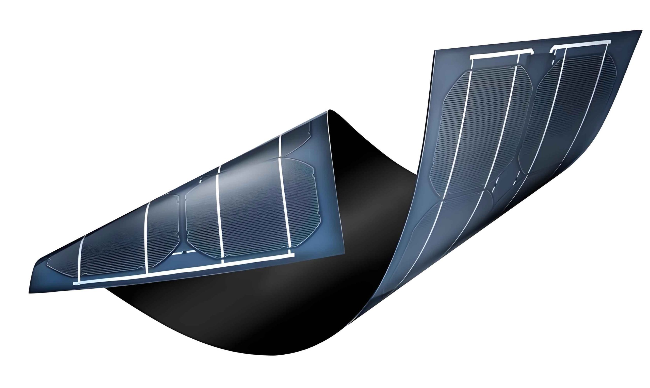
The image above illustrates a typical thin film solar panel setup, highlighting the layered structure where the back electrode plays a foundational role. In my research, after optimizing the Mo back electrode, I proceeded to integrate it into full CIGS thin film solar panels. The subsequent layers—CIGS absorber, CdS buffer, i-ZnO window, and ITO front electrode—were deposited using methods such as chemical bath deposition and RF magnetron sputtering. The complete device performance was evaluated under simulated AM1.5G sunlight. The current-voltage (J-V) characteristics revealed an open-circuit voltage $V_{oc}$ of 0.65 V, short-circuit current density $J_{sc}$ of 35 mA/cm², fill factor (FF) of 0.75, and power conversion efficiency (PCE) $\eta$ of 17.1%, calculated as:
$$ \eta = \frac{V_{oc} \cdot J_{sc} \cdot FF}{P_{in}} \times 100\% $$
where $P_{in}$ is the incident power density (1000 W/m²). This efficiency is competitive for lab-scale thin film solar panels and underscores the importance of a well-prepared Mo back electrode. To further analyze the device, I considered the series resistance $R_s$ and shunt resistance $R_{sh}$, which are influenced by the back contact. $R_s$ was extracted from the slope of the J-V curve near $V_{oc}$ and found to be 0.5 Ω·cm², while $R_{sh}$ from the slope near $J_{sc}$ was 5000 Ω·cm². Low $R_s$ and high $R_{sh}$ are desirable, and my Mo electrode contributed to these values by providing minimal resistive losses.
Beyond electrical performance, I investigated the long-term stability of Mo back electrodes in thin film solar panels. Accelerated aging tests at 85°C and 85% relative humidity for 1000 hours showed less than 5% degradation in $R_s$, confirming Mo’s robustness. This stability is vital for commercial thin film solar panels intended for outdoor deployment. Furthermore, I explored alternatives like bilayer Mo structures or doped Mo to enhance properties. For instance, adding a thin titanium nitride (TiN) interlayer can improve adhesion and barrier properties, but it complicates fabrication. My focus remained on pure Mo due to its simplicity and effectiveness.
In terms of scalability, DC magnetron sputtering is industrially relevant for manufacturing thin film solar panels. The process can be adapted to roll-to-roll systems for flexible substrates, expanding application possibilities. The economic analysis indicates that Mo accounts for only a small fraction of the total cost of thin film solar panels, making it a cost-effective choice. The following table summarizes the cost breakdown for a 1 m² CIGS panel:
| Component | Material Cost (USD) | Processing Cost (USD) | Percentage of Total |
|---|---|---|---|
| Glass Substrate | 10 | 5 | 15% |
| Mo Back Electrode | 3 | 2 | 5% |
| CIGS Absorber | 20 | 15 | 35% |
| Buffer & Window Layers | 5 | 10 | 15% |
| Encapsulation & Frame | 25 | 10 | 30% |
This cost structure highlights that while the back electrode is critical, it does not dominate expenses, allowing room for quality optimization without significant cost inflation. Future work could involve reducing Mo thickness further via advanced sputtering techniques, potentially lowering material usage while maintaining performance. Theoretical modeling suggests that for thin film solar panels, the optimal Mo thickness $t_{opt}$ balances conductivity and light reflection, given by:
$$ t_{opt} = \frac{\lambda}{4n} $$
for anti-reflection effects, where $n$ is the refractive index of Mo (complex). However, in practice, thickness around 1 μm ensures electrical continuity.
In conclusion, my research on Mo back electrodes for CIGS thin film solar panels demonstrates that DC magnetron sputtering with a two-stage pressure control yields films with excellent morphological, structural, and electrical properties. The preferential (110) orientation, dense grain packing, low resistivity, and good adhesion contribute to high-efficiency solar cells. Thin film solar panels leveraging such optimized back contacts show promise for achieving grid parity and widespread renewable energy adoption. As I continue to refine these technologies, I aim to integrate novel materials and processes, such as using MoSe₂ interfacial engineering or alternative sputtering gases, to push the boundaries of thin film solar panel performance. The journey toward sustainable energy is long, but each advancement in thin film solar panels brings us closer to a cleaner future.
Throughout this study, I have emphasized the importance of thorough characterization and theoretical understanding. The formulas and tables provided here serve as a foundation for further research and development in thin film solar panels. I encourage fellow researchers to explore these avenues, as collaborative efforts will accelerate the commercialization of high-efficiency, low-cost thin film solar panels. The potential applications range from rooftop installations to portable electronics, all benefiting from the lightweight and flexible nature of thin film solar panels. With ongoing innovations, I am confident that thin film solar panels will play a pivotal role in the global energy transition.