
1. Introduction
The global energy transition toward sustainability has intensified the demand for efficient and reliable power conversion systems. Traditional diesel generators, despite their widespread use, suffer from noise pollution, environmental hazards, and inefficiency. In contrast, energy storage inverters offer a clean, compact, and high-efficiency alternative. This paper focuses on the design and analysis of a single-phase energy storage inverter with a two-stage architecture: a front-end push-pull DC-DC converter and a rear-end full-bridge inverter. The system addresses critical challenges in voltage stabilization, switching losses, thermal management, and control strategy optimization.
2. Front-End Push-Pull DC-DC Converter
2.1 Topology and Operating Principles
The push-pull converter (Figure 1) employs a center-tapped transformer to achieve voltage amplification and galvanic isolation. Key components include MOSFETs T1 and T2, resonant capacitors Cr, and leakage inductances Ls1 and Ls2. The converter operates in three distinct modes:
- ZVS Turn-On (t0−t1): T1 conducts with zero voltage, leveraging transformer leakage inductance and resonant capacitance.
- Dead Time (t1−t2): Both switches are off; parasitic capacitors charge/discharge to prepare T2 for ZVS.
- ZCS Turn-Off (t2−t3): T2 turns off at zero current, minimizing switching losses.
The resonant frequency fr and switching frequency fs are governed by:fr=2πLsCr1,fs<fr
where Ls=Ls1=Ls2. This ensures soft-switching across varying loads.
2.2 Modeling and Control
Using the First Harmonic Approximation (FHA), the converter’s equivalent circuit (Figure 2) simplifies analysis by considering only the fundamental harmonic. The voltage gain M is expressed as:M=UinUout=1+Q2(frfs−fsfr)2n1
where Q=Req2πfrLs is the quality factor, and Req represents the load reflected to the primary side.
A voltage feedback loop with a PI controller (transfer function GT(s)) stabilizes the DC bus voltage:GT(s)=Kp(1+Tis1)
The SG3525 PWM controller generates complementary gate signals, ensuring precise duty cycle regulation.
2.3 Hardware Design
- Transformer: An EE42 core with 6 primary turns (40 strands of 0.6 mm wire) and 9 secondary turns (36 strands of 0.4 mm wire) minimizes core losses.
- Switches: IRF150P220AKMA1 MOSFETs (150 V, 203 A) handle voltage/current stresses.
- Rectification: EPU3006 ultrafast diodes (600 V, 30 A) ensure low reverse recovery losses.
3. Rear-End Full-Bridge Inverter
3.1 Topology and Modulation
The full-bridge inverter (Figure 3) converts the boosted DC voltage into 220 V/50 Hz AC. Switching states (Table 1) define four operational modes:
| Switch States (S1−S4) | Output Voltage (Uout) |
|---|---|
| 1001 | +Udc |
| 0110 | −Udc |
| 0000/1111 | 0 |
Unipolar SPWM modulation doubles the effective switching frequency, reducing harmonic distortion.
3.2 Dual-Loop Control Strategy
A voltage-current dual-loop control (Figure 4) enhances dynamic response:
- Inner Current Loop:
Gi(s)=sLf+Rfkpwmks
where kpwm is the PWM gain, Lf and Rf are filter parameters.
- Outer Voltage Loop:
Gv(s)=s(1+Tps)kp(1+Tzs)
Bode plots (Figure 5) validate stability margins (≥45∘ phase margin).
3.3 Loss Optimization
A low-frequency modulation strategy reduces switching losses by operating one bridge arm at 50 Hz and the other at 20 kHz. Conduction and switching losses are modeled as:Pcon=VCEIavg+Irms2Ron,Psw=Ts1∫0Ts(Eon+Eoff)dt
where Eon/off are energy losses per switching cycle.
4. Thermal and Loss Analysis
4.1 Power Device Loss Models
IGBT and diode losses are temperature-dependent:VCE(T)=V0,L(25∘C)+Kv0,L(Tj−25),Ron(T)=RL(25∘C)+Kr,L(Tj−25)
Thermal impedance networks (Figure 6) predict junction temperatures:ΔT=Ptotal⋅(Rth,jc+Rth,ch+Rth,ha)
4.2 Simulation and Validation
PLECS simulations (Table 2) confirm 92.3% efficiency at full load. Thermal imaging (Figure 7) shows peak temperatures below 85°C, validating heat sink design.
5. Experimental Results
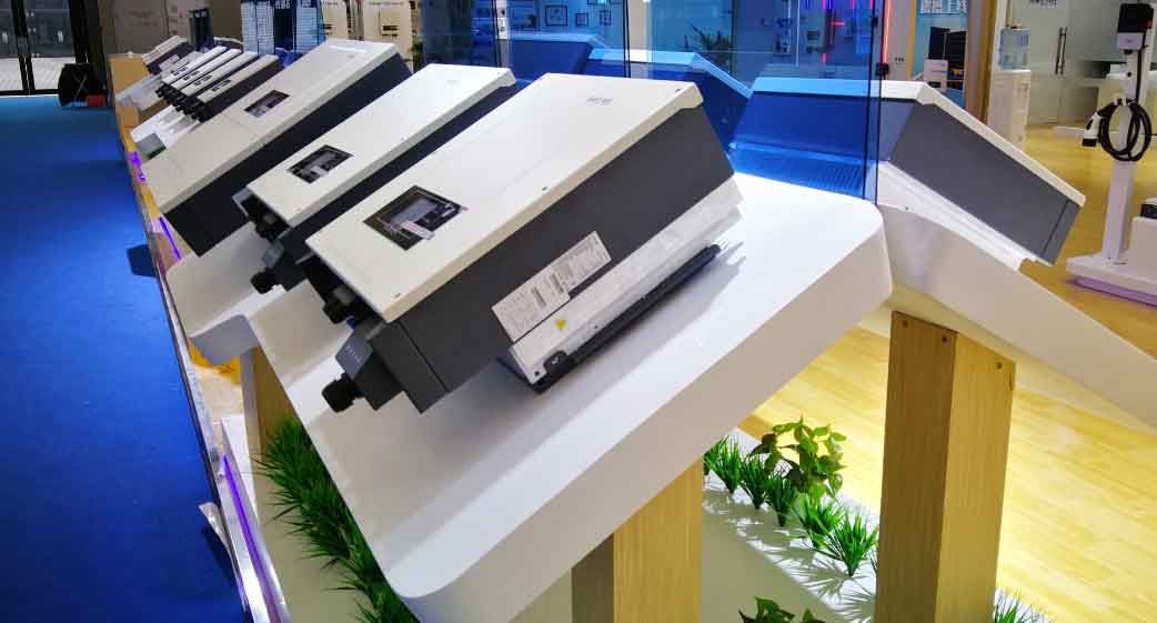
A 2 kW prototype (Figure 8) with TMS320F28335 DSP control demonstrates:
- THD: <2.5% under linear/nonlinear loads.
- Voltage Regulation: ±1.2% deviation during 0–100% load steps.
- Efficiency: 91.7% at rated power (Table 3).
6. Conclusion
This work presents a comprehensive methodology for designing high-efficiency single-phase energy storage inverters. Key innovations include:
- Soft-switching push-pull converter with LC resonance.
- Dual-loop control for robust voltage/current regulation.
- Loss-optimized modulation and thermal management.
Future work will explore wide-bandgap devices (SiC/GaN) for higher switching frequencies and bidirectional power flow capabilities.