
In my research, I focus on the reliability of the solar inverter because it is the most fragile link in a photovoltaic power system. Although photovoltaic modules can operate for more than 25 years, the solar inverter often requires replacement or major repair within 5 to 8 years. The solar inverter performs dc–ac conversion, grid synchronization, maximum power point tracking, and protection functions. Its failure directly reduces energy yield, increases maintenance cost, and weakens grid stability. Among the internal components of a solar inverter, the insulated-gate bipolar transistor (IGBT) module and the dc-link capacitor are the two most critical reliability bottlenecks. In this work, I combine electrical, thermal, and statistical methods to study the solar inverter from the system level down to the semiconductor device level, and I also propose a practical method to forecast the power loss caused by inverter failure.
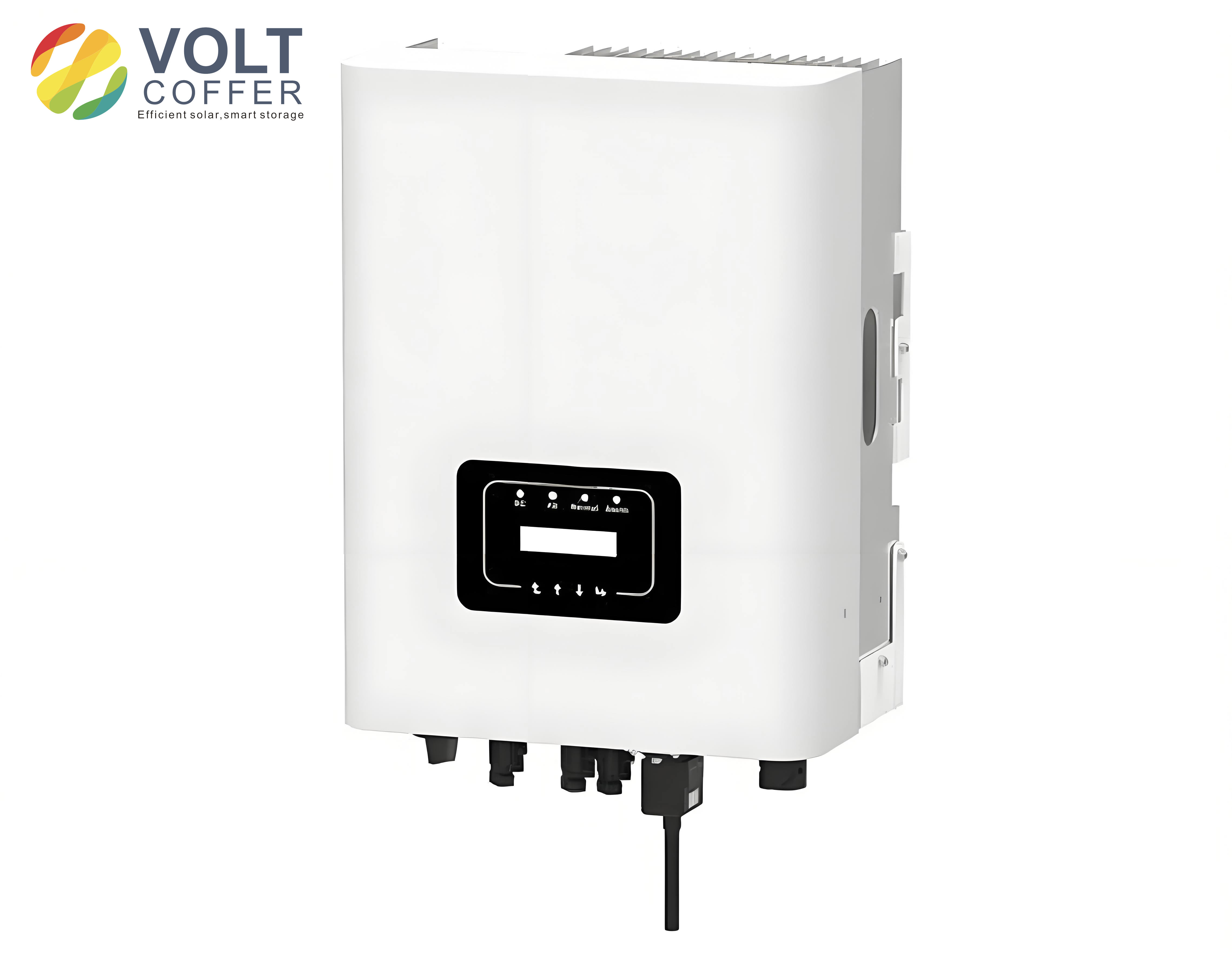
A solar inverter is not a simple dc–ac converter. It must match the photovoltaic array in voltage, current, and power. If the match is poor, the solar inverter either operates in a low-efficiency region or limits the array output. Therefore, I first analyze the selection principles of a solar inverter and then narrow the discussion to IGBT selection inside the solar inverter. This system-level perspective is important because the reliability of the solar inverter cannot be improved only by choosing a high-quality semiconductor; the operating point, thermal environment, and mission profile also determine its lifetime.
For a single-phase solar inverter, the dc-link capacitor must buffer the double-frequency power ripple. A first-order design equation for the required capacitance is
$$C_R \ge \frac{P_{PV}}{2 \omega_{grid} U_C \hat{u}_C}$$
where \(P_{PV}\) is the rated photovoltaic power, \(\omega_{grid}\) is the grid angular frequency, \(U_C\) is the average dc-link voltage, and \(\hat{u}_C\) is the allowed voltage ripple. This equation assumes that the photovoltaic current is nearly dc, the inverter output current follows a sinusoidal form, and the average dc-link voltage is constant. In practice, electrolytic capacitors are widely used because they provide large capacitance at low cost, but their lifetime is limited. At 105 °C, an electrolytic capacitor may last only 1000 to 5000 hours. Because a solar inverter is often installed outdoors, the thermal stress is severe, and the capacitor becomes a dominant failure location. Replacing electrolytic capacitors with film capacitors or other long-life capacitors can improve solar inverter reliability, but the capacitance value is usually smaller, so the control and filtering design must be re-examined.
The conversion efficiency of a solar inverter is defined as the ratio of ac output energy to dc input energy:
$$\eta = \frac{E_{AC}}{E_{DC}} = \frac{\int P_{AC}(t)dt}{\int P_{DC}(t)dt}$$
Two widely used weighted efficiencies are the European efficiency and the California efficiency. The European efficiency is
$$\eta_{EU} = 0.03\eta_{5\%} + 0.06\eta_{10\%} + 0.13\eta_{20\%} + 0.10\eta_{30\%} + 0.48\eta_{50\%} + 0.20\eta_{100\%}$$
and the California efficiency is often written as
$$\eta_{CAL} = 0.04\eta_{10\%} + 0.05\eta_{20\%} + 0.12\eta_{30\%} + 0.21\eta_{50\%} + 0.53\eta_{75\%} + 0.05\eta_{100\%}$$
These weighted efficiencies show that the solar inverter spends most of its time at partial load. If the inverter is oversized, it operates too often at very low power, where efficiency is poor. If it is undersized, it clips the array output during high irradiance. Therefore, the selection of a solar inverter must consider the actual irradiance profile, the array configuration, and the thermal environment.
I use a 6 kW photovoltaic array as an example. The array consists of monocrystalline silicon modules. The module parameters are listed in Table 1. Two candidate solar inverters with the same rated power but different input voltage windows are compared in Table 2. The goal is to determine the feasible series and parallel connection of modules for each solar inverter.
| Parameter | Value |
|---|---|
| Open-circuit voltage | 60.0 V |
| Maximum power voltage | 48.9 V |
| Short-circuit current | 5.6 A |
| Maximum power current | 5.32 A |
| Peak power | 260 Wp |
| Temperature coefficient of open-circuit voltage | −0.43%/°C |
| Temperature coefficient of short-circuit current | −0.34%/°C |
| Cell type | Monocrystalline silicon |
| Solar inverter | Model | Input voltage window | Maximum input voltage | Maximum input current |
|---|---|---|---|---|
| Inverter A | SG5KTL-D | 240–520 V | 600 V | 22 A |
| Inverter B | SG5KTL-EC | 280–800 V | 1000 V | 19.8 A |
For the module, the maximum power voltage at 60 °C is
$$V_{mpp,60} = 48.9 + (-0.0043)(60-25) \times 48.9 \approx 41.5 \text{ V}$$
and the open-circuit voltage at −10 °C is
$$V_{oc,-10} = 60.0 + (-0.0043)(-10-25) \times 60.0 \approx 69.0 \text{ V}$$
For Inverter A, the minimum number of series modules is
$$N_{s,min} = \frac{240}{41.5} \approx 5.8 \rightarrow 6$$
and the maximum number of series modules is
$$N_{s,max} = \frac{600}{69.0} \approx 8.7 \rightarrow 8$$
Thus, 6 to 8 modules can be connected in series. If 6 modules are in series and 4 strings are in parallel, the total number of modules is 24, the total power is 24 × 260 W = 6.24 kW, and the current is 4 × 5.32 A = 21.3 A, which is below the 22 A limit. The inverter-to-array ratio is 5 kW / 6.24 kW = 0.80. If 6 modules are in series and 3 strings are in parallel, the total power is 18 × 260 W = 4.68 kW, and the current is 3 × 5.32 A = 16.0 A. The ratio is 5 kW / 4.68 kW = 1.07, which is also acceptable.
For Inverter B, the minimum number of series modules is
$$N_{s,min} = \frac{280}{41.5} \approx 6.7 \rightarrow 7$$
and the maximum number of series modules is
$$N_{s,max} = \frac{1000}{69.0} \approx 14.5 \rightarrow 14$$
If 7 modules are in series and 3 strings are in parallel, the total power is 21 × 260 W = 5.46 kW, and the current is 16.0 A, which is below 19.8 A. The ratio is 5 kW / 5.46 kW = 0.92. If 7 modules are in series and 4 strings are in parallel, the current is 21.3 A, which exceeds the 19.8 A limit, so this configuration is not feasible. This example shows that voltage and current windows directly determine the feasible array layout, and the solar inverter must be selected together with the array topology.
Once the solar inverter is selected, the IGBT inside the solar inverter must be chosen. IGBTs combine the low on-state resistance of a bipolar transistor with the high input impedance of a MOSFET. In a solar inverter, the IGBT operates in a pulse-width-modulated full-bridge or three-phase bridge. The IGBT is switched at frequencies from about 10 kHz to 20 kHz, and the switching loss becomes a major part of the total loss. The IGBT types include punch-through (PT), non-punch-through (NPT), soft punch-through (SPT), and trench-gate field-stop structures. Table 3 summarizes the main features.
| IGBT type | Key feature | Typical advantage | Typical limitation |
|---|---|---|---|
| PT-IGBT | n+ buffer layer on p+ substrate | Low on-state voltage | Higher switching loss, temperature-sensitive saturation voltage |
| NPT-IGBT | Thin n− drift region without buffer | Positive temperature coefficient, rugged short-circuit behavior | Higher on-state voltage |
| SPT-IGBT | Soft punch-through field-stop layer | Thin wafer, low loss, good ruggedness | Optimized design required |
| Trench field-stop IGBT | Vertical trench gate and field-stop layer | High current density, low saturation voltage | More complex fabrication |
For a solar inverter, the IGBT must be able to withstand the dc-link voltage, the repetitive peak current, and the short-circuit current. It must also have a low saturation voltage and low switching energy. The safe operating area (SOA) of the IGBT is divided into three regions: high-voltage low-current, high-current low-voltage, and high-voltage high-current. The last region is limited by thermal heating. In a solar inverter, the IGBT experiences both conduction loss and switching loss. The total loss is
$$P_{tot} = P_{cond} + P_{sw} + P_{drive}$$
where \(P_{cond}\) is conduction loss, \(P_{sw}\) is switching loss, and \(P_{drive}\) is gate-drive loss. The conduction loss of an IGBT can be approximated as
$$P_{cond} = V_{CE0} I_C + r_C I_C^2$$
and the conduction loss of the anti-parallel diode is
$$P_{cond,D} = V_{F0} I_F + r_F I_F^2$$
where \(V_{CE0}\) and \(V_{F0}\) are threshold voltages, and \(r_C\) and \(r_F\) are on-state resistances. The switching loss of the IGBT is
$$P_{sw} = f_{sw} \left( E_{on} + E_{off} \right) \frac{V_{DC}}{V_{ref}} \left[ 1 + \alpha_T (T_j – T_{ref}) \right]$$
where \(f_{sw}\) is the switching frequency, \(E_{on}\) and \(E_{off}\) are turn-on and turn-off energies at the reference voltage \(V_{ref}\), \(V_{DC}\) is the dc-link voltage, \(T_j\) is the junction temperature, and \(\alpha_T\) is the temperature coefficient. For the diode, the reverse recovery loss is
$$P_{rr} = f_{sw} E_{rr} \frac{V_{DC}}{V_{ref}} \left[ 1 + \alpha_T (T_j – T_{ref}) \right]$$
In a full-bridge solar inverter, four IGBTs and four diodes are used. By symmetry, I only need to calculate the loss of one IGBT and one diode, and then multiply by four. For a three-phase solar inverter, the multiplier is six. The average loss over one fundamental period is
$$P_{av} = \frac{1}{T} \int_0^T P_{tot}(t) dt$$
The junction temperature is then calculated from the thermal network. I use both Foster and Cauer networks. The Foster network represents the transient thermal impedance as a sum of exponential terms:
$$Z_{th}(t) = \sum_{i=1}^{n} R_i \left( 1 – e^{-t/\tau_i} \right)$$
where \(\tau_i = R_i C_i\). The Cauer network represents the physical layers of the IGBT module. The two networks are mathematically equivalent, but the Foster network is easier to extract from finite-element simulation or measurement. The steady-state thermal resistance is
$$R_{th} = \sum_{i=1}^{n} R_i$$
The junction temperature rise is
$$\Delta T_j = P_{av} \left( Z_{thjc} + Z_{thch} + Z_{thha} \right)$$
where \(Z_{thjc}\) is the junction-to-case impedance, \(Z_{thch}\) is the case-to-heatsink impedance, and \(Z_{thha}\) is the heatsink-to-ambient impedance. The average junction temperature is
$$T_{j,av} = T_a + P_{av} R_{th,total}$$
To obtain accurate thermal parameters, I build a finite-element model of an IGBT module. I choose a 600 V / 75 A IGBT module as the object. The module is a wire-bonded package with a silicon chip, solder layer, direct-bonded copper (DBC) ceramic, baseplate, thermal grease, and heatsink. The material properties are listed in Table 4.
| Layer | Material | Thermal conductivity (W/m·K) | Specific heat (J/kg·K) | Density (kg/m³) | Thickness (mm) |
|---|---|---|---|---|---|
| IGBT chip | Si | Temperature-dependent | Temperature-dependent | 2330 | 0.18 |
| Diode chip | Si | Temperature-dependent | Temperature-dependent | 2330 | 0.38 |
| Chip solder | SnAg3.5 | 57 | 226 | 7400 | 0.08 |
| DBC copper | Cu | 390 | 380 | 8800 | 0.30 |
| DBC ceramic | Al₂O₃ | 22 | 830 | 3864 | 0.32 |
| Baseplate solder | SnCu3In0.1 | 57 | 242 | 7400 | 0.08 |
| Baseplate | Cu | 390 | 380 | 8800 | 3.00 |
For silicon, the thermal conductivity and specific heat are temperature-dependent. I use the following approximations:
$$k_{Si}(T) = \frac{1}{0.00156 + 0.0000133 T}$$
$$c_{Si}(T) = 0.1626 + 0.000425 T$$
where \(T\) is in Kelvin. In the finite-element model, I apply a volumetric heat source to the IGBT chip, use a convective coefficient of 10 W/m²·K on the side surfaces, and use a convective coefficient of 5000 W/m²·K on the bottom of the baseplate to represent a heatsink. The transient thermal impedance is extracted from the simulated junction temperature rise divided by the applied power. The simulated steady-state thermal resistance is 0.34 K/W, while the product datasheet gives 0.35 K/W. The relative error is
$$\frac{0.35 – 0.34}{0.35} \times 100\% = 2.86\%$$
which validates the finite-element model. The fitted transient thermal impedance of the IGBT chip is
$$Z_{thjc}(t) = 0.218(1 – e^{-t/0.0012}) + 0.105(1 – e^{-t/0.075})$$
where the time constants are obtained from the fitted \(R_i C_i\) products. The corresponding thermal resistances and capacitances are listed in Table 5.
| Parameter | R₁ (K/W) | C₁ (J/K) | R₂ (K/W) | C₂ (J/K) |
|---|---|---|---|---|
| IGBT chip | 0.218 | 0.0055 | 0.105 | 0.712 |
For the thermal grease and heatsink, I use published transient thermal impedance curves and fit them with the same exponential form. The heatsink and thermal grease parameters are listed in Table 6. The heatsink geometry and material properties are listed in Table 7 and Table 8.
| Parameter | R₁ (K/W) | C₁ (J/K) | R₂ (K/W) | C₂ (J/K) | R₃ (K/W) | C₃ (J/K) | R₄ (K/W) | C₄ (J/K) |
|---|---|---|---|---|---|---|---|---|
| Thermal grease | 0.00302 | 0.271 | 0.00430 | 0.562 | 0.00039 | 0.577 | 0.00021 | 0.925 |
| Heatsink | 0.1044 | 344.4 | 0.0496 | 20.56 | 0.3699 | 1634 | — | — |
| Parameter | W (mm) | L (mm) | H (mm) | m | n | k (mm) | h (mm) |
|---|---|---|---|---|---|---|---|
| Value | 140 | 390 | 50 | 4 | 3.55 | 3.55 | 5 |
| Component | Material | Thermal conductivity (W/m·K) | Specific heat (J/kg·K) | Density (kg/m³) |
|---|---|---|---|---|
| Heatsink | Aluminum | 237 | 903 | 2702 |
| Thermal grease | — | 1 | 753 | 2810 |
After obtaining the thermal network, I build an electro-thermal coupling model in MATLAB Simulink. The model represents the power loss as a current source and the thermal impedances as RC networks. The ambient temperature is a voltage source. The average power loss is calculated from the datasheet energies:
$$P_{av} = \frac{1}{T} \sum_{k=1}^{N_{sw}} \left( E_{on,k} + E_{off,k} + E_{rr,k} \right)$$
For a 50 Hz output, I use a sinusoidal half-wave power loss as the input. The peak value of the equivalent current source is
$$I_{peak} = \frac{\pi P_{av}}{2}$$
With an average power loss of 55 W, the peak current is about 86.4 A. The simulation runs until the junction temperature reaches steady state. The simulated average junction temperature is compared with the theoretical value:
$$T_{j,av} = T_a + P_{av} \left( R_{thjc} + R_{thch} + R_{thha} \right)$$
Using \(R_{thjc} = 0.35\) K/W, \(R_{thch} = 0.009\) K/W, and \(R_{thha} = 0.52\) K/W, the total thermal resistance is 0.879 K/W. If the ambient temperature is 25 °C, the theoretical average junction temperature is
$$T_{j,av} = 25 + 55 \times 0.879 = 73.3 \text{ °C}$$
The simulated average junction temperature is within 1.36% of this value, which confirms that the electro-thermal model is reliable.
Once the junction temperature is known, I can estimate the IGBT lifetime. The lifetime of an IGBT module is limited by power cycling fatigue. The most widely used model is the LESIT model:
$$N_f = A \Delta T_j^{\alpha} e^{E_a / (k_B T_{jm})}$$
where \(N_f\) is the number of cycles to failure, \(\Delta T_j\) is the junction temperature swing, \(T_{jm}\) is the mean junction temperature, \(k_B\) is Boltzmann’s constant, and \(A\), \(\alpha\), and \(E_a\) are model parameters. For the LESIT model, typical values are \(A = 3.025 \times 10^5\), \(\alpha = -5.039\), and \(E_a = 9.891 \times 10^{-20}\) J. A more comprehensive model includes the effects of pulse width, bond wire current, voltage class, and bond wire diameter:
$$N_f = A \Delta T_j^{\beta_1} T_{j,min}^{\beta_2} t_{on}^{\beta_3} I_B^{\beta_4} V_C^{\beta_5} D^{\beta_6}$$
The parameters for this model are listed in Table 9. For a 600 V / 75 A IGBT module, I use the measured bond wire diameter and the datasheet current. The junction temperature swing is obtained from the electro-thermal simulation. For a 20 s power cycle, the simulated minimum junction temperature is 45 °C and the maximum is 66 °C, so \(\Delta T_j = 21\) K. The pulse width is 10 s. Using the modified model, I calculate the number of cycles to failure. For a 50 Hz fundamental output, the actual pulse width is \(t_{on} = 0.02/2 = 0.01\) s, and the corresponding lifetime is obtained by scaling the cycle count. This lifetime is used as a reference for maintenance scheduling of the solar inverter.
| Parameter | Symbol | Unit | Range | Coefficient | Value |
|---|---|---|---|---|---|
| Technology factor | A | — | — | — | 2.03 × 10¹⁴ (standard), 9.34 × 10¹⁴ (IGBT4) |
| Temperature swing | ΔT_j | K | 45–150 | β₁ | −4.416 |
| Minimum chip temperature | T_j,min | °C | 20–120 | β₂ | 1285 |
| Pulse width | t_on | s | 1–15 | β₃ | −0.463 |
| Bond wire current | I_B | A | 3–32 | β₄ | −0.716 |
| Voltage class / 100 | V_C | V | 6–33 | β₅ | −0.761 |
| Bond wire diameter | D | μm | 75–500 | β₆ | −0.5 |
Besides lifetime prediction, I also study the consequences of solar inverter failure. When a solar inverter trips, the energy that would have been generated during the downtime is lost. Forecasting this loss is important for grid operators and asset managers. I propose a statistical method based on the correlation between historical generation data of different solar inverters in the same plant. The correlation coefficient between two inverters \(i\) and \(j\) is
$$r_{ij} = \frac{\sum_{t=1}^{N} (E_i(t) – \bar{E}_i)(E_j(t) – \bar{E}_j)}{\sqrt{\sum_{t=1}^{N} (E_i(t) – \bar{E}_i)^2} \sqrt{\sum_{t=1}^{N} (E_j(t) – \bar{E}_j)^2}}$$
If inverter \(i\) fails, I use the inverter \(j\) with the highest correlation to forecast the lost energy:
$$\hat{E}_i(t) = E_j(t) \frac{P_{rated,i}}{P_{rated,j}}$$
The absolute percentage error is
$$APE(t) = \left| \frac{\hat{E}_i(t) – E_i(t)}{E_i(t)} \right| \times 100\%$$
I validate this method using data from a 2.38 MW photovoltaic plant with 79 string inverters. The data cover two months. I test time resolutions of one hour, one day, and one week. Table 10 shows the hourly prediction results. When the correlation coefficient is about 99.9%, the hourly average error is still around 10%, which is not accurate enough for industrial use. Table 11 shows the daily prediction results. When the correlation coefficient is above 99.9%, the average error is below 10%, which is acceptable. Table 12 shows the weekly prediction results. When the correlation coefficient is above 99.9%, the average error is below 3%, which is very accurate. I also test a second plant and obtain consistent conclusions.
| Plant | Faulty solar inverter | Reference solar inverter | Correlation coefficient | Average hourly error |
|---|---|---|---|---|
| Plant A | Inverter 1 | Inverter 2 | 99.87% | 9.82% |
| Plant A | Inverter 20 | Inverter 21 | 99.89% | 10.44% |
| Plant B | Inverter 8B | Inverter 8A | 99.96% | 2.28% |
| Plant | Faulty solar inverter | Reference solar inverter | Correlation coefficient | Average daily error |
|---|---|---|---|---|
| Plant A | Inverter 1 | Inverter 2 | 99.93% | 5.44% |
| Plant A | Inverter 1 | Inverter 6 | 95.33% | 10.22% |
| Plant A | Inverter 20 | Inverter 21 | 99.88% | 8.12% |
| Plant A | Inverter 20 | Inverter 4 | 95.09% | 16.79% |
| Plant B | Inverter 8B | Inverter 7A | 99.98% | 1.10% |
| Plant | Faulty solar inverter | Reference solar inverter | Correlation coefficient | Average weekly error |
|---|---|---|---|---|
| Plant A | Inverter 1 | Inverter 2 | 99.91% | 2.46% |
| Plant A | Inverter 1 | Inverter 39 | 91.82% | 11.13% |
| Plant A | Inverter 1 | Inverter 29 | 81.73% | 23.38% |
| Plant A | Inverter 20 | Inverter 21 | 99.99% | 8.78% |
| Plant A | Inverter 20 | Inverter 7 | 90.45% | 13.51% |
| Plant A | Inverter 20 | Inverter 16 | 80.28% | 18.15% |
| Plant B | Inverter 8B | Inverter 12B | 99.99% | 2.00% |
The results show that the correlation-based method is suitable for daily and weekly forecasting when the correlation coefficient is above 99.9%. For hourly forecasting, the error is too large because the generation of a solar inverter is highly volatile at short time scales. The method is simple, data-driven, and does not require irradiance or temperature measurements. It can be integrated into a monitoring system for a solar inverter fleet.
In summary, I have studied the solar inverter reliability from three perspectives. First, I analyzed the selection and matching of the solar inverter with the photovoltaic array, including voltage, current, power, and efficiency considerations. Second, I built a thermal network of the IGBT module and extracted the transient thermal impedance using finite-element analysis. The simulated steady-state thermal resistance differed from the datasheet by only 2.86%. Third, I built an electro-thermal coupling model in MATLAB Simulink and predicted the IGBT lifetime using both the LESIT model and a modified power-cycling model. The simulated average junction temperature agreed with the theoretical value within 1.36%. Finally, I proposed a correlation-based method to forecast the power loss caused by solar inverter failure. The method was validated with real data from two photovoltaic plants. The daily and weekly forecasts were accurate when the correlation coefficient was above 99.9%, while hourly forecasts were not reliable enough for industrial use.
For future work, I recommend three directions. The first is to replace electrolytic capacitors with long-life film capacitors or other advanced capacitors to improve solar inverter reliability. The second is to develop more efficient cooling methods, such as phase-change cooling or double-sided cooling, to reduce the IGBT junction temperature and extend its lifetime. The third is to combine machine learning with the correlation-based method to improve short-term forecasting of solar inverter failure losses. These improvements will help the solar inverter achieve higher reliability, lower maintenance cost, and better grid support.
The methods and results presented here can be used by engineers and researchers who work on solar inverter design, thermal management, lifetime prediction, and photovoltaic plant operation. The thermal network and electro-thermal model can be extended to three-phase solar inverters and multi-chip IGBT modules. The forecasting method can be implemented in a supervisory control and data acquisition system to estimate lost generation after a solar inverter trip. In this way, the reliability of the solar inverter and the profitability of the photovoltaic plant can be improved together.
I also note that the solar inverter is a complex system, and its reliability is affected by many factors, including mission profile, ambient temperature, humidity, dust, grid voltage, and control strategy. A complete reliability assessment should combine physics-of-failure models with field data. In my work, I have taken a step in this direction by linking semiconductor-level thermal analysis with system-level generation forecasting. The equations and tables provided here can serve as a reference for further studies on solar inverter reliability and fault-induced power loss prediction.