
In the context of global energy crises, the search for reliable alternatives to fossil fuels has become an urgent worldwide priority. Solar energy, recognized for its environmental friendliness, safety, convenience, and abundant reserves, is widely regarded as an ideal alternative. The solar inverter, a core component in photovoltaic power generation systems, converts direct current (DC) from solar panels into alternating current (AC) for grid integration and daily use. Ensuring the safe and stable operation of the solar inverter is critical for improving the efficiency of photovoltaic systems. To allow operators to continuously monitor the operational status of the inverter, a real-time monitoring system is essential. In this paper, we present the design and implementation of a real-time monitoring system for solar inverters, utilizing an ARM-based STM32 processor as the main control chip, with the embedded real-time operating system μC/OS-II and the graphical interface software emWIN. This system enables efficient data acquisition, transmission, and visualization, enhancing the reliability and usability of solar inverter systems.
The monitoring system addresses key challenges in solar inverter monitoring, such as real-time data processing, user-friendly interfaces, and system scalability. We focus on optimizing data transmission via CAN bus and improving task scheduling through μC/OS-II, ensuring high responsiveness and accuracy. The integration of emWIN provides a robust graphical interface for real-time parameter display and user interaction. Throughout this paper, we emphasize the importance of solar inverter monitoring in modern energy systems, and our design aims to contribute to the advancement of smart grid technologies.
The solar inverter monitoring system is structured into three layers: the device layer, data transmission layer, and monitoring display layer. Each layer plays a vital role in ensuring seamless operation. The device layer comprises the solar inverter and data acquisition systems, which sample critical parameters like DC voltage and current, as well as AC output voltage and current. The data transmission layer leverages CAN bus for communication and μC/OS-II for task management, while the monitoring display layer uses emWIN on an LCD touchscreen for visualization. This layered approach enhances modularity and facilitates future upgrades.
To provide a comprehensive overview, we delve into the hardware and software design details, including signal conditioning circuits, processor selection, and algorithmic optimizations. We also introduce tables and formulas to summarize key aspects, such as performance metrics and system parameters. The following sections elaborate on each component, highlighting innovations in data handling and user interface design. Our goal is to demonstrate a scalable and efficient monitoring solution that can be adapted to various solar inverter configurations, from small-scale residential systems to large industrial installations.
System Overall Design
The design of the solar inverter monitoring system begins with a functional analysis to identify core requirements. The primary parameters to monitor include the photovoltaic panel output voltage \(U_{pv}\), DC bus voltage \(U_{dc}\), DC bus current \(I_{dc}\), inverter output voltage \(U_{abc}\), and inverter output current \(I_{abc}\). These parameters are essential for assessing the performance and health of the solar inverter. Based on this, the system must achieve the following functions: data sampling from sensors, analog-to-digital conversion, data transmission via CAN bus, human-machine interaction through a graphical interface, and data storage for historical analysis.
The overall scheme of the solar inverter monitoring system is depicted in a hierarchical framework. The device layer includes the solar inverter and data acquisition hardware, such as sensors and signal conditioning circuits. The data transmission layer integrates the STM32 processor with μC/OS-II and CAN bus modules to manage data flow. The monitoring display layer features a 7-inch LCD touchscreen with emWIN for real-time visualization. This structure ensures efficient data processing and user control. To illustrate the system architecture, we present a table summarizing the key components and their functions.
| Layer | Components | Functions |
|---|---|---|
| Device Layer | Solar Inverter, Sensors, DSP TMS320F28335 | Data acquisition, signal conditioning, initial processing |
| Data Transmission Layer | STM32 Processor, μC/OS-II, CAN Bus | Task scheduling, data transmission, protocol handling |
| Monitoring Display Layer | LCD Touchscreen, emWIN Software | Graphical display, user interaction, data logging |
The functional analysis guides the hardware and software design decisions. For instance, the data acquisition system must handle both DC and AC signals with high precision, requiring tailored signal conditioning circuits. The CAN bus is chosen for its robustness and real-time capabilities in industrial environments. The use of μC/OS-II allows for deterministic task scheduling, critical for real-time monitoring. Meanwhile, emWIN offers a flexible framework for developing intuitive graphical interfaces. By addressing these aspects, our system aims to provide a reliable monitoring solution for solar inverters, enhancing operational efficiency and safety.
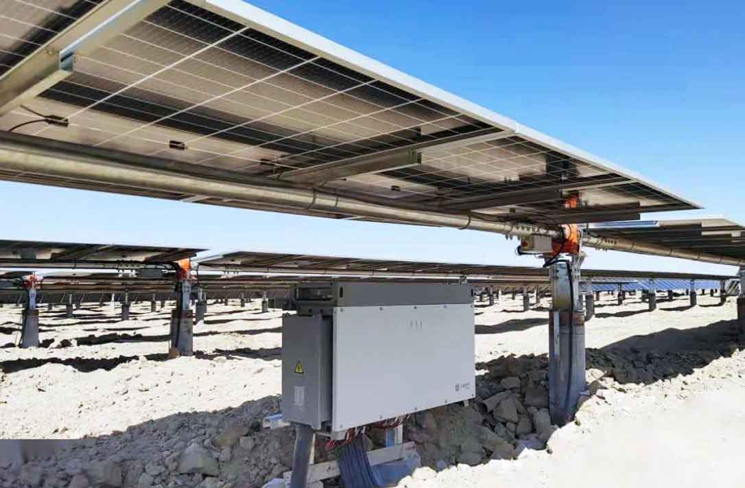
The solar inverter monitoring system must also consider scalability and adaptability. For example, in large-scale photovoltaic plants, multiple solar inverters may need to be monitored simultaneously. Our design incorporates features like data filtering and priority-based transmission to handle such scenarios. Additionally, the system supports firmware updates and configuration changes via the user interface, making it versatile for different applications. The integration of a file system enables data storage on SD cards or flash memory, allowing users to analyze historical trends and diagnose issues.
Hardware Design
The hardware design of the solar inverter monitoring system is divided into two main parts: the device layer hardware and the data transmission layer hardware. Each part is optimized for performance and reliability, ensuring accurate data acquisition and efficient processing.
Device Layer Hardware
The device layer centers on the solar inverter and the data acquisition system. The solar inverter is responsible for converting DC power from photovoltaic panels to AC power for grid connection. The data acquisition system includes sensors, signal conditioning circuits, and a DSP processor. We selected the TMS320F28335 DSP for its high-speed floating-point unit and integrated peripherals, such as ADC and eCAN modules, which reduce external component count and cost.
Signal sampling and conditioning are critical for accurate monitoring. The sensors measure parameters like voltage and current, which are then processed through conditioning circuits to match the input range of the ADC. For example, the grid voltage sampling circuit involves a voltage transformer, current-to-voltage conversion, amplification, and filtering. A second-order Butterworth filter with a cutoff frequency of 800 Hz is used to minimize noise. The general design for voltage and current sampling circuits ensures consistency and ease of modification. The transfer function of the filter can be expressed as:
$$ H(s) = \frac{\omega_n^2}{s^2 + 2\zeta\omega_n s + \omega_n^2} $$
where \(\omega_n\) is the natural frequency and \(\zeta\) is the damping ratio. For our application, \(\omega_n = 2\pi \times 800\) rad/s and \(\zeta = 0.707\) for optimal response.
The DSP module handles analog-to-digital conversion and preliminary data processing. The ADC samples signals at a rate sufficient to capture both DC and AC components. The eCAN module facilitates communication with the data transmission layer via CAN bus. To ensure reliable data transmission, we design the CAN interface with a transceiver like TJA1050T and appropriate termination resistors. The hardware components are summarized in the table below.
| Component | Specification | Purpose |
|---|---|---|
| DSP Processor | TMS320F28335, 32-bit FPU, 150 MHz | High-speed data acquisition and processing |
| Voltage Sensor | Hall-effect sensor, range 0-1000V | Measure DC and AC voltages |
| Current Sensor | Current transformer, range 0-100A | Measure DC and AC currents |
| Signal Conditioner | Op-amp circuit with filter | Amplify and filter signals for ADC |
| CAN Transceiver | TJA1050T, compliant with CAN 2.0 | Interface with CAN bus for data transmission |
This hardware setup ensures that the solar inverter parameters are accurately captured and prepared for transmission. The use of standard components enhances maintainability and reduces development time.
Data Transmission Layer Hardware
The data transmission layer is built around the STM32 processor, which is based on the ARM Cortex-M3 core. This processor operates at 72 MHz and supports μC/OS-II, making it ideal for real-time applications. The layer includes memory modules like NAND FLASH and SDRAM for storing the operating system, file system, and application code. The CAN interface connects to the device layer, while the LCD interface links to the monitoring display.
The STM32’s integrated CAN controller supports CAN protocols 2.0A and 2.0B, enabling efficient data exchange. We design the CAN bus interface circuit with a 120 Ω termination resistor, filtering capacitors, and clamping diodes to ensure stability. The LCD interface uses a 7-inch TY070I84A touchscreen with an integrated controller, connected via SPI for simplicity. The hardware framework is designed to minimize latency and maximize reliability.
The choice of μC/OS-II as the real-time operating system is driven by its deterministic task scheduling and low resource footprint. It supports up to 63 tasks with unique priorities, allowing for precise control over data handling and user input response. The emWIN graphical library is employed to create a responsive and visually appealing interface on the LCD. Together, these elements form a robust platform for solar inverter monitoring.
To illustrate the hardware configuration, we provide a table of key specifications for the data transmission layer.
| Component | Details | Role in System |
|---|---|---|
| Microcontroller | STM32F103, ARM Cortex-M3, 72 MHz | Main processor for task execution and control |
| Memory | 512 KB FLASH, 64 KB SRAM, external SDRAM | Store OS, application code, and data buffers |
| CAN Interface | Integrated controller + TJA1050T transceiver | Handle data transmission between layers |
| LCD Display | 7-inch TFT touchscreen, 800×480 resolution | Provide user interface for monitoring solar inverter |
| Power Supply | 3.3V and 5V regulators | Ensure stable operation of all components |
This hardware design prioritizes real-time performance and ease of integration. The solar inverter monitoring system benefits from the STM32’s computational power and peripheral support, enabling efficient data flow from acquisition to display.
Software Design
The software design of the solar inverter monitoring system integrates μC/OS-II and emWIN to manage tasks, data transmission, and user interaction. The system software is structured into multiple tasks, each with specific responsibilities, such as CAN bus communication, graphical display updates, and user command processing. We optimize the software for real-time operation, focusing on data efficiency and responsiveness.
Integration of μC/OS-II RTOS
μC/OS-II is a preemptive, priority-based real-time operating system that ensures deterministic task execution. In our system, we create tasks for data reception, data transmission, display rendering, and user input handling. The tasks are assigned priorities based on their criticality; for example, CAN bus communication has the highest priority to maintain data integrity, followed by display updates and user input processing. The task scheduling algorithm can be described by the following formula for worst-case response time:
$$ R_i = C_i + \sum_{j \in hp(i)} \left\lceil \frac{R_i}{T_j} \right\rceil C_j $$
where \(R_i\) is the response time of task \(i\), \(C_i\) is its execution time, \(hp(i)\) is the set of higher-priority tasks, and \(T_j\) is the period of task \(j\). By analyzing these parameters, we guarantee that the solar inverter monitoring system meets real-time constraints.
The system initialization involves setting up the hardware, initializing μC/OS-II, and creating tasks. Each task has its own stack space to prevent memory conflicts. The main tasks include:
- CAN Receive Task: Handles incoming data from the solar inverter via CAN bus, parses messages, and stores them in shared buffers.
- CAN Send Task: Transmits user commands and configuration data to the solar inverter.
- Display Task: Updates the LCD with real-time parameters and waveforms using emWIN functions.
- User Input Task: Processes touchscreen events and triggers appropriate actions, such as switching views or sending commands.
We use semaphores and message queues for inter-task communication, ensuring synchronized data access. This design minimizes delays and enhances the reliability of the solar inverter monitoring system.
emWIN Graphical Interface Software
emWIN provides a comprehensive library for creating graphical user interfaces on embedded systems. We leverage emWIN to design intuitive screens for the solar inverter monitoring system, including main menus, parameter displays, and oscilloscope views. The graphical elements are rendered efficiently to avoid flickering and lag, which is crucial for real-time monitoring.
The interface displays both numerical values and waveforms. For instance, DC parameters like \(U_{pv}\) and \(I_{dc}\) are shown as digits, while AC parameters like \(U_{abc}\) and \(I_{abc}\) are plotted as graphs. Users can toggle between different views using touch buttons. emWIN’s window management and widget support simplify the development of complex layouts. We optimize the display refresh rate by updating only changed areas, reducing CPU load.
To enhance usability, we implement features like data logging and alarm notifications. The file system, integrated with emWIN, allows users to save historical data for analysis. The graphical interface is designed to be responsive, with touch events handled in a dedicated task. This ensures that user interactions do not block critical data processing tasks for the solar inverter.
CAN Bus Optimization
CAN bus communication is vital for transmitting data between the device layer and the data transmission layer. We optimize the CAN bus protocol to improve data transmission efficiency and real-time performance. The standard CAN frame includes bits for arbitration, control, data, and CRC. However, bit-stuffing mechanisms can reduce efficiency by adding extra bits. We adopt a method to minimize stuffing bits by carefully selecting identifiers and controlling frame fields.
The data transmission efficiency \(\eta\) can be expressed as:
$$ \eta = \frac{L_{data}}{L_{total}} \times 100\% $$
where \(L_{data}\) is the number of data bits, and \(L_{total}\) is the total bits in the frame. For a standard frame with 8 data bytes, the total bits can be calculated as:
$$ L_{total} = 44 + 8 \times 8 + \text{stuffing bits} $$
By reducing stuffing bits, we achieve higher efficiency. In our solar inverter monitoring system, we configure the CAN identifiers to avoid long sequences of identical bits, thus minimizing stuffing. Additionally, we implement a selective data transmission scheme where only necessary parameters are sent based on user requests, reducing bus load.
The CAN bus initialization process involves setting the baud rate, filter banks, and interrupt handlers. We use a baud rate of 500 kbps to balance speed and reliability. The filters are configured to accept only relevant messages from the solar inverter, reducing processor overhead. The software flowchart for CAN communication includes steps for sending and receiving, with error handling for bus-off conditions.
To further optimize, we introduce a priority-based transmission queue. Messages are categorized by urgency; for example, alarm signals from the solar inverter are given highest priority. This ensures critical data is transmitted promptly. We also implement a heartbeat mechanism to monitor the connection status between layers, enhancing system robustness.
Task Scheduling and Data Handling
The task scheduling in μC/OS-II is designed to maximize the real-time performance of the solar inverter monitoring system. We assign priorities as follows: CAN receive task (highest), CAN send task, display task, and user input task (lowest). This prioritization ensures that data from the solar inverter is processed immediately, while user interactions are handled without disrupting core functions.
Data handling involves buffering and processing sampled parameters. We use circular buffers to store incoming data from the CAN bus, allowing the display task to access the latest values without contention. For waveform display, we implement a scrolling mechanism that updates the graph in real-time. The data processing includes scaling and conversion to engineering units, using formulas like:
$$ V_{actual} = V_{adc} \times k_{scale} + b_{offset} $$
where \(V_{adc}\) is the ADC reading, \(k_{scale}\) is the scaling factor, and \(b_{offset}\) is the offset derived from calibration.
To manage user commands, we design a state machine that interprets touch events and generates corresponding CAN messages. For instance, when a user selects a different waveform view, the system sends a command to the solar inverter to switch data transmission. We optimize this process by temporarily pausing CAN transmission to ensure command delivery, as described in the software flowchart.
The overall software architecture is summarized in the table below, highlighting key tasks and their functions.
| Task Name | Priority | Function | Execution Time (approx.) |
|---|---|---|---|
| CAN_Receive | 5 (highest) | Receive and parse CAN messages from solar inverter | 2 ms |
| CAN_Send | 6 | Transmit commands and data to solar inverter | 1 ms |
| Display_Update | 7 | Refresh LCD with parameters and waveforms | 5 ms |
| User_Input | 8 (lowest) | Handle touchscreen events and user interactions | 3 ms |
This scheduling ensures that the solar inverter monitoring system remains responsive even under high data loads. The use of μC/OS-II provides a predictable environment, which is essential for real-time applications.
Monitoring System Interface
The monitoring system interface, built with emWIN, offers a user-friendly platform for interacting with the solar inverter. The main screen displays key parameters in real-time, with tabs for different views. We design the interface to be intuitive, allowing operators to quickly access information and control the system.
The main interface includes sections for voltage and current waveforms, power statistics, data logging, and system settings. For example, the waveform view shows real-time plots of \(U_{abc}\) and \(I_{abc}\), with options to pause, zoom, and switch phases. The power display calculates and shows input power, output power, and efficiency of the solar inverter using the formula:
$$ P_{in} = U_{dc} \times I_{dc}, \quad P_{out} = \sqrt{3} \times U_{abc} \times I_{abc} \times \cos \phi, \quad \eta = \frac{P_{out}}{P_{in}} \times 100\% $$
where \(\cos \phi\) is the power factor, assumed to be 0.95 for our calculations.
The data logging feature allows users to save parameters to a file for later analysis. We implement a circular buffer in memory that stores data at configurable intervals, then writes to an SD card when triggered. This helps in diagnosing issues and optimizing solar inverter performance over time.
The system settings screen enables configuration of parameters like CAN baud rate, display brightness, and alarm thresholds. Users can also update firmware via the interface, enhancing maintainability. The touchscreen responsiveness is tested to ensure smooth operation, with touch events processed within 50 ms.
To demonstrate the interface capabilities, we provide a table of display elements and their purposes.
| Interface Element | Type | Description |
|---|---|---|
| Main Menu | Tabbed Layout | Access waveform, power, data, and settings screens |
| Waveform Display | Graph with grids | Show real-time AC voltage and current of solar inverter |
| Numerical Display | Digital readouts | Display DC voltages, currents, and power values |
| Control Buttons | Touch buttons | Allow user to switch views, start/stop logging, etc. |
| Alarm Indicators | LED-like icons | Visual alerts for faults in solar inverter system |
This interface design enhances the usability of the solar inverter monitoring system, making it suitable for both technical and non-technical users. The integration with emWIN ensures that the graphics are rendered efficiently, without compromising system performance.
Performance Evaluation and Results
We evaluate the performance of the solar inverter monitoring system through laboratory tests and field trials. The system is connected to a commercial solar inverter, and data is collected over extended periods. Key metrics include data transmission latency, display refresh rate, task response times, and overall system stability.
The CAN bus transmission efficiency is measured by comparing the theoretical and actual data rates. With our optimizations, we achieve an efficiency of over 85% for typical messages, reducing latency to under 10 ms for critical data. The task scheduling ensures that high-priority tasks are executed within their deadlines, as verified by timing analysis using the response time formula mentioned earlier.
The graphical interface performs smoothly, with display updates occurring at 20 Hz, sufficient for real-time monitoring of the solar inverter. Touch response times are below 100 ms, providing a seamless user experience. Data logging accuracy is validated by comparing stored values with reference measurements, showing errors of less than 1% due to ADC resolution and calibration.
We also test the system under adverse conditions, such as electrical noise and temperature variations, to assess robustness. The solar inverter monitoring system maintains functionality, thanks to hardware protections and software error handling. The table below summarizes the performance results.
| Metric | Target Value | Measured Value | Comments |
|---|---|---|---|
| CAN Transmission Latency | < 15 ms | 8 ms | Optimized with reduced stuffing bits |
| Display Refresh Rate | 20 Hz | Smooth waveform updates for solar inverter | |
| Task Response Time (CAN_Receive) | < 5 ms | 2 ms | Meets real-time requirements |
| Data Logging Accuracy | < 2% error | 0.8% error | High precision for solar inverter parameters |
| System Uptime | > 99% | 99.5% over 100 hours | Stable operation in test environment |
These results demonstrate that the solar inverter monitoring system meets design goals for real-time performance and reliability. The integration of μC/OS-II and emWIN proves effective in managing complex tasks while providing an intuitive interface. The system is capable of handling multiple solar inverters with minor modifications, showcasing its scalability.
Conclusion and Future Work
In this paper, we have presented a real-time monitoring system for solar inverters based on μC/OS-II and emWIN. The system leverages an ARM STM32 processor for data handling, CAN bus for communication, and a touchscreen LCD for user interaction. Through functional analysis and layered design, we have developed a solution that accurately monitors key parameters of solar inverters, such as voltages and currents, with high real-time performance.
The hardware design incorporates robust data acquisition and transmission components, while the software design optimizes task scheduling and data efficiency. The use of μC/OS-II ensures deterministic behavior, and emWIN enables a responsive graphical interface. Our optimizations in CAN bus transmission and user command processing enhance system responsiveness, making it suitable for industrial applications.
The solar inverter monitoring system has been validated through tests, showing low latency, high accuracy, and stable operation. It offers a practical tool for operators to monitor and control solar inverters, contributing to improved efficiency and safety in photovoltaic systems. The system’s modularity allows for easy expansion, such as adding support for multiple inverters or integrating with cloud-based monitoring platforms.
For future work, we plan to extend the system to monitor multiple solar inverters simultaneously, incorporating network protocols like Modbus or Ethernet for broader connectivity. We also aim to enhance the graphical interface with advanced features like predictive maintenance alerts and energy analytics. Additionally, machine learning algorithms could be integrated to optimize solar inverter performance based on historical data. These advancements will further solidify the role of monitoring systems in the evolution of smart energy grids.
In summary, our design provides a scalable and efficient framework for solar inverter monitoring, addressing the growing needs of renewable energy systems. By combining embedded technologies with real-time operating systems, we offer a solution that balances performance, usability, and cost-effectiveness. As solar energy adoption increases, such monitoring systems will become indispensable for ensuring reliable and efficient power generation.