
On the basis of completing the design of the portable power supply system scheme, FSBB converter, inverter circuit control strategy research, and the entire system software and hardware design, the various modules of the portable power supply system will be integrated, and the experimental device and testing platform of the portable mobile power supply system will be built. Experimental verification will be carried out based on the theoretical analysis mentioned earlier. By analyzing the experimental waveforms and data, verify whether the performance indicators of the system meet the expected requirements, verify the feasibility of the portable power supply system solution, and assemble the entire system equipment.
1. Experimental platform construction and modular testing
Based on the control strategy and key research on software and hardware mentioned earlier, use Altium Designer software to draw PCB and schematic diagrams for each module and print out the physical board. Using the existing equipment in the laboratory, build corresponding experimental platforms and verify whether the performance of each module meets the design requirements through the waveform and numerical values of the oscilloscope.
1.1 FSBB Charging Module Testing and Analysis
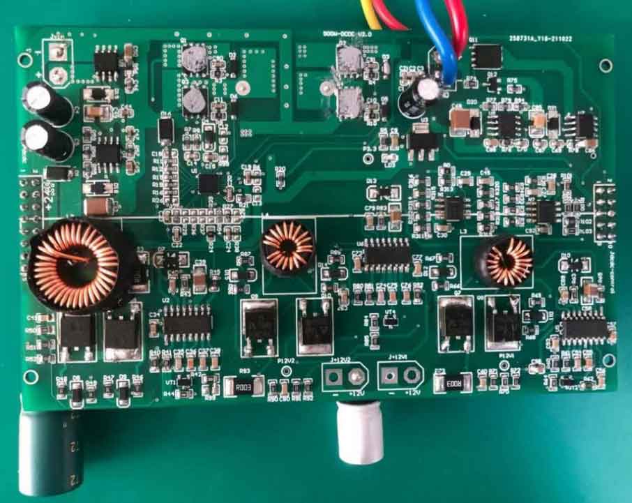
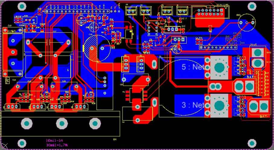
Firstly, based on the hardware design of the control board for the charging module in Chapter 4, draw and print the PCB of the FSBB converter control board, as shown in Figures 1 and 2.

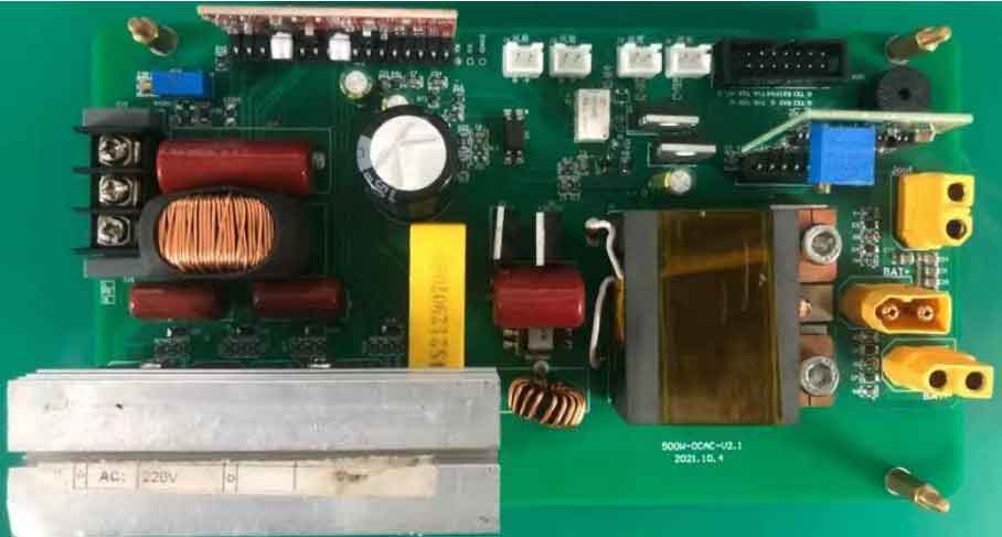
After the circuit board is soldered with components, the FSBB experimental prototype is built for testing based on the analysis of the three mode control strategy of FSBB, as shown in Figure 3. Using a linear power supply to power the FSBB control board, a four channel oscilloscope detects the waveforms of each of the four MOS transistors, observes whether the control signal of the MOS transistor can work normally within the input voltage range required by the experiment, and observes the input and output voltage waveforms and values to verify whether the voltage stabilization accuracy of the output voltage is less than 2% when the input voltage suddenly changes.
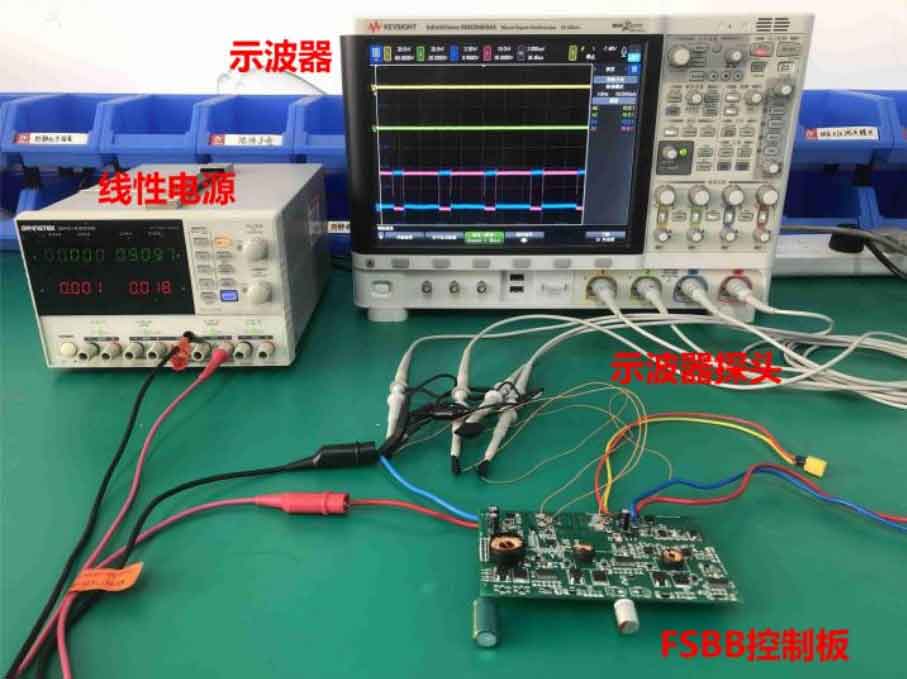
Connect the four probes of the oscilloscope to four MOS tubes, and provide input voltages of 24V, 12V, and 8V with a linear power supply. Place the FSBB converter in three modes: Buck, Buck Boost, and Boost. Observe the MOS tube driving waveform through the oscilloscope, as shown in Figures 4, 5, and 6.
As shown in Figures 4, 5, and 6, the four MOS transistors can conduct in the order required by the design, and the switching process is stable. Connect the oscilloscope probe to the output terminal and input terminal (linear power supply) of the FSBB converter, momentarily change the input voltage, and observe the output voltage waveform, as shown in Figures 7 and 8.
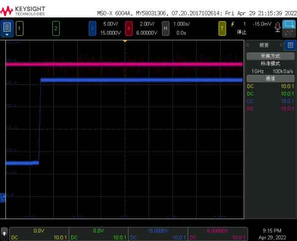
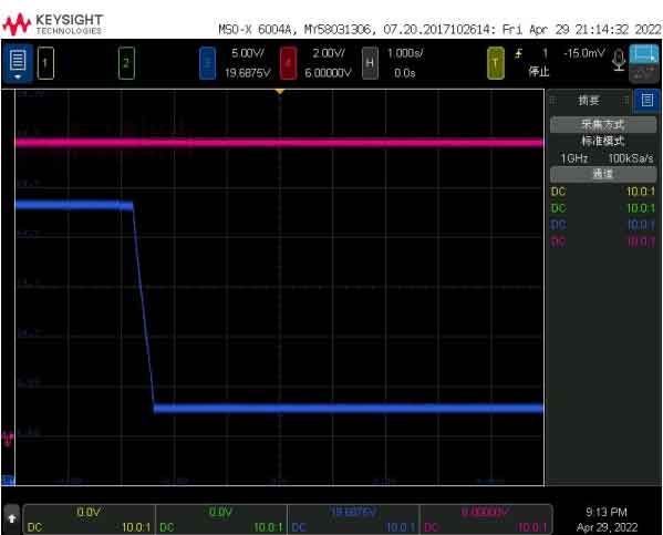
From Figures 7 and 8, it can be seen that regardless of whether the output voltage is an instantaneous change from low voltage to high voltage or from high voltage to low voltage, as long as it is within the input voltage range, the waveform of the output voltage remains stable near the set value. The maximum fluctuation range of the output voltage waveform read from the oscilloscope is 11.8V-12.2V. Use the following equation to calculate the voltage stabilization accuracy:

Among them, δ U represents the voltage stabilization accuracy, Umax represents the limit value of output voltage fluctuation, and UZ represents the output voltage setting value. According to the calculation of equation (6.1), the voltage stabilization accuracy is less than 1.7%, which proves that the design scheme effectively solves the problem of wide range voltage input, and the mode switching process is stable. The stability of the portable power supply system is good, which meets the experimental expectations.
1.2 Testing and analysis of full bridge inverter discharge module
According to the hardware design of the control board for the discharge module in Chapter 4, draw and print the PCBs for the front and rear stages of the AC output, as shown in Figures 9 and 10.
After soldering the components, an experimental prototype of the inverter circuit was constructed based on voltage fuzzy PID control strategy analysis. According to the national power quality requirements, as shown in Table 1, test whether the performance indicators of the power frequency voltage output by the portable power supply system meet the requirements.
| Power quality category | Frequency deviation | Voltage deviation | Total harmonic distortion rate |
| Performance requirements | ± 0.5Hz | +7%, -10% | 5.0 |
As shown in Figures 11 and 12, a lithium battery pack is used to power the inverter circuit control board, and the oscilloscope uses a high-voltage probe to detect the various values of the output waveform of the experimental prototype.
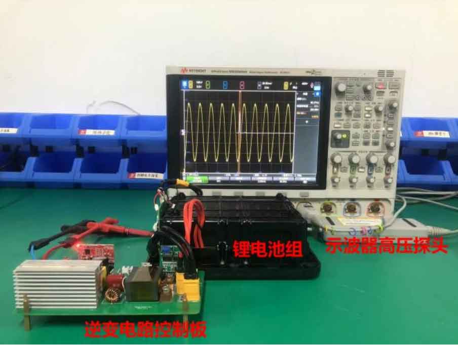
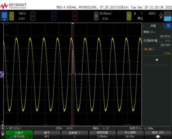
The displayed values of the oscilloscope in Figure 12 indicate the frequency, amplitude, and total harmonic distortion distortion (THD) of the current output voltage. Record a set of data every 10 seconds and obtain experimental results through 20 measurements:
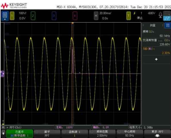
The voltage output waveform of the portable power supply system when unloaded is a standard sine wave, with an output voltage amplitude range of 212-226V and a voltage deviation of+3% and -4%; The waveform frequency range is 49.95Hz-50.15Hz, with a frequency deviation of ± 0.2. Using the built-in digital function of the oscilloscope, perform Fast Fourier Transform (FFT) on the output waveform, set the center frequency to 50Hz and the frequency range to 2kHz, and obtain a THD of 1.56% at no-load. The above three indicators meet the requirements of no-load design. After testing the no-load performance indicators of the portable power supply system, connect a 500W blower to the output voltage interface and observe the performance indicators of the output waveform of the portable power supply system when loaded.
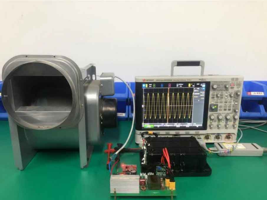
Similar to the analysis of no-load data, another 20 data collections were conducted on the loaded system. The analysis results showed that when the portable power supply system was loaded, the amplitude and frequency of the output voltage still fluctuated within the range of no-load testing, and the THD of the output waveform was 2.53%, slightly increased compared to no-load but still less than the specified indicators.
The experimental results show that regardless of whether it is unloaded or loaded, the output waveform of the experimental prototype is not distorted, and the amplitude and frequency stability of the output voltage are good, proving that the control strategy of this module meets the expected experimental requirements.
2. Portable power supply system overall testing
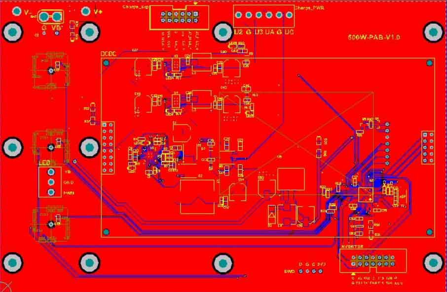
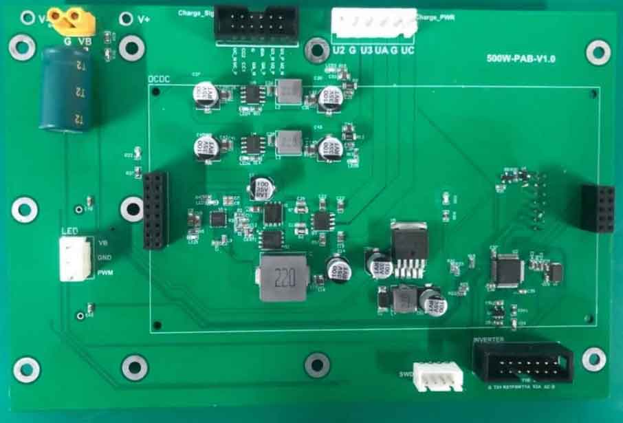
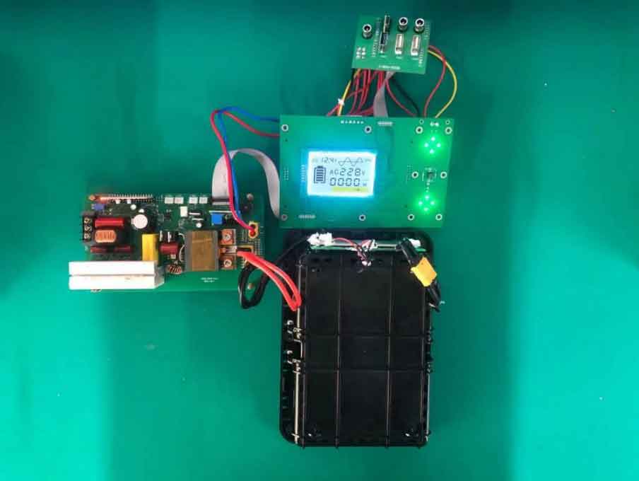
After performance testing of the input and output key modules of the portable power supply system, all modules were wired and assembled to form a complete portable mobile power supply prototype. The power management module was used to test the other modules. The PCB and physical components of the power management module control board are shown in Figures 15 and 16.
After soldering the power management control board onto the LCD display screen, connect each module as a whole, as shown in Figure 17. Display the current operating status of the portable power system through the readings on the LCD screen, and conduct tests in sequence.
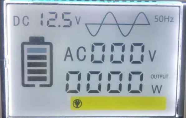
(1) Portable power system charging test:
Connect the charger to the charging port to charge the portable power supply system, as shown in Figure 18. The charging label below the LCD display screen lights up, and the current battery voltage is displayed in the upper left corner. When the displayed value is 12.6V, the battery is fully charged. After a period of testing, the portable power supply system’s charging status is normal and stable, proving that the charging module design of the system meets the experimental requirements.
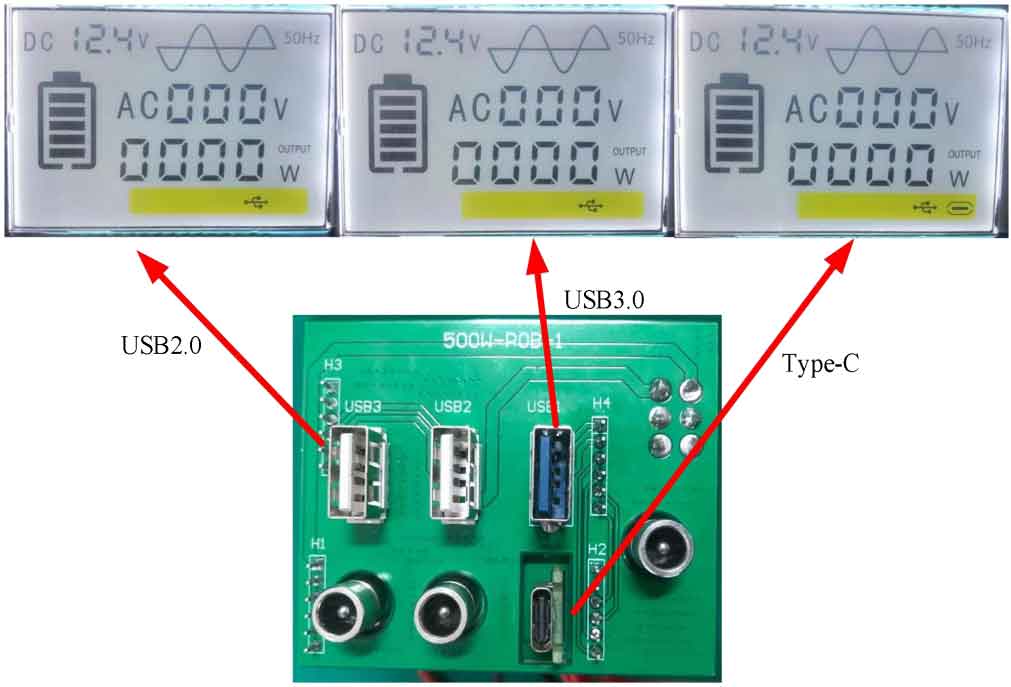
(2) DC discharge test:
After activating the DC discharge button, the DC discharge module of the portable power system starts to work, as shown in Figure 19. The smart phone is charged using the USB2.0, USB3.0, and Type-C socket interfaces in sequence. Based on 20% of the remaining battery of the mobile phone, charging tests were conducted sequentially, with charging times of 2 hours, 0.9 hours, and 0.9 hours, respectively. Due to different fast charging protocols of the USB interface, the charging time varies, but stable DC output voltage can be provided normally, indicating that the design of the portable power system DC discharge module meets the experimental requirements.
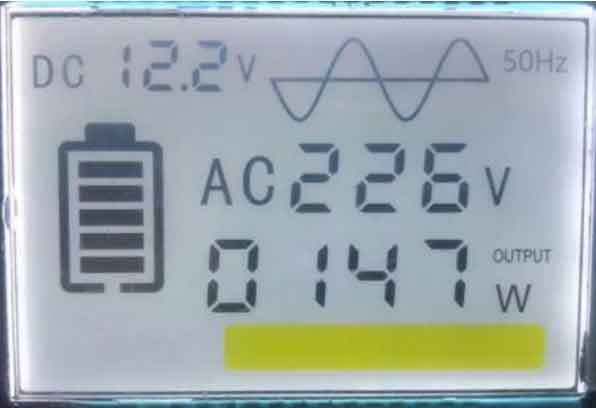
(3) AC discharge test:
After activating the AC discharge button, the AC discharge module of the portable power supply system begins to work. The load device is connected to the AC output interface, as shown in Figure 20. The LCD screen displays the current AC voltage amplitude and output power output by the system. After a period of testing, the load device can work normally within the specified parameter range of the portable power supply system without displaying any alarm information, proving that the design of the AC discharge module of the portable power supply system meets the experimental requirements.
3. Summary
Firstly, the assembly of the experimental device and the construction of the experimental platform were completed in modules, and experimental testing was carried out according to the design scheme. Through the analysis of experimental waveforms and data, the accuracy of the control strategy was proven. Then, each module was assembled into a complete prototype and subjected to overall charging and discharging tests on the portable power supply system, verifying its practicality.