
with the increasing scarcity of fossil fuels, we need to find new energy sources to replace them. Solar energy is receiving increasing attention from scientists due to its renewable and clean characteristics. We have now turned our attention to solar photovoltaic grid connected power generation, which eliminates bulky, expensive, and difficult to maintain batteries and directly connects the generated electricity to the grid for practical use. The main equipment for photovoltaic grid connected power generation is the grid connected inverter, which plays a great role in improving photovoltaic power generation efficiency and reducing costs. Photovoltaic grid connected power generation will become the main development direction of photovoltaic power generation systems with the rapid development of solar technology. And its main device, the grid connected inverter, has a critical impact on the safe, reliable, and efficient operation of the photovoltaic grid connected power generation system. The photovoltaic power generation system we currently use mainly converts solar energy into electrical energy and stores it in a battery, which is then directly supplied to the load. The advantages of this system are its simple structure and low cost, while its disadvantage is that the different DC voltage of the load makes it difficult to achieve standardization and compatibility of the system, especially for civil power, which is mostly AC load. Therefore, this system is difficult to be utilized in the real market. In addition, with the development of society, powerful models must be adopted to achieve grid connected operation of photovoltaic power generation, which will push the AC photovoltaic power generation system into the mainstream of the photovoltaic power generation field.
1. Introduction
1.1 Question raising
Inversion, which refers to DC/AC, and rectification, which refers to AC/DC, both act in the system where DC power supplies AC loads. One of the main research topics for scientists now is photovoltaic inverters using photovoltaic cells. The design of this course is to use 10KW photovoltaic cells as energy sources and use PWM control
The inverter circuit obtains a single-phase AC stable power supply of 220V/4.5A.
1.2 Proposal
Option 1: In this design, we can use digital methods to generate PWM waves (i.e. by programming to generate PWM waves), thus achieving the design of the photovoltaic inverter.
This scheme uses a microcontroller (microcontroller) to achieve PWM modulation, and the PWM wave can be programmed through the microcontroller. The output PWM wave can be adjusted at any time through the program; The protection circuit in this scheme is achieved by connecting the output value of the sampling circuit to an A/D converter for A/D conversion, and then sending the conversion result to the microcontroller for protection through a program.
Option 2: From the design requirements, it can be seen that this is the production of a photovoltaic inverter. We can use analog circuits and integrated PWM controllers to achieve this photovoltaic inverter.
This scheme is a photovoltaic inverter implemented using full hardware circuits, where the PWM controller uses SG3525 and its corresponding peripheral circuits to achieve PWM modulation. The voltage feedback circuit can feedback the output voltage at any time, and adjust the PWM wave output to meet the requirements through SG3525. The protection circuit is implemented using analog electronic technology.
1.3 Demonstration of the plan
Among the two options above, we choose the second option. In the first scheme, we use a microcontroller to achieve PWM modulation, which can be achieved through software. Although this modulation and hardware circuit are simple, the cost is relatively high. In the second scheme, we use an analog method to achieve PWM modulation. PWM modulation uses a dedicated PWM control chip SG3525, which uses SG3525 and its corresponding peripheral circuits to achieve PWM modulation. The PWM wave generation method here is based on modulation rather than calculation, as the calculation method is relatively complex. The modulation method used in this design can fully meet the design requirements, so SG3525 was chosen to modulate and generate PWM waves. The modulation here adopts an asynchronous modulation method, where the carrier frequency remains fixed and unchanged, i.e. the carrier ratio N changes when changing. By connecting the feedback end of SG3525 to the feedback signal, real-time adjustment can be made to meet the needs when the output signal changes.
The voltage feedback circuit can feedback the output voltage at any time, and adjust the PWM wave output through SG3525 to meet the requirements. This chip is cheap and applicable, and it is easy to buy in the market. The corresponding circuit is also relatively simple, because SG3525 itself has an external shutdown signal input terminal, and the frequency of oscillation can be changed by changing the external oscillation resistance and capacitance of SG3525, thereby changing the output PWM wave.
2. Operating characteristics of photovoltaic arrays
2.1 Photocells
When exposed to sunlight, a photovoltaic cell spontaneously generates a directional photoelectric electromotive force. If it is connected to a path without a power source at this time, there will be current flowing through it. We are now familiar with many types of photocells, including selenium, cuprous oxide, thallium sulfide, cadmium sulfide, germanium, silicon, gallium arsenide, etc. Silicon photocells are widely used in production and real life due to their advantages of high temperature resistance and stability, and are the most well-known. In addition, according to the fact that the peak value of the silicon spectrum is within the visual range of the human eye, we also use it to manufacture analytical instruments, measuring instruments, and other equipment.
2.2 Working principle
Due to the need to generate a PN junction in silicon photocells, some P-type impurities need to be incorporated into it. When the P-region is illuminated, if the energy of photons reaches a certain level that is greater than the bandgap width of silicon, an electron hole pair will be generated in the P-region. The more photons are absorbed in the P-region, a large number of electron holes will be generated, and the electron holes generated further away from the surface will gradually decrease. This difference will form a natural trend of diffusion from the surface to the interior according to a certain pattern. Because the electric field inside the PN junction points from the N region to the P region, the attraction separates the electron hole pairs, causing the N region to adsorb electrons while the P region absorbs a large number of holes. In this way, the P region will be positively charged and the N region will be negatively charged, resulting in a potential difference and the generation of electromotive force. At this point, connect the two zones into one
Path, there will be current flowing through the circuit.
2.3 Working characteristics
2.3.1 Spectral characteristics
The wavelength of light is different, and the sensitivity of photocells to it is also different. The range of incident light waves corresponding to photovoltaic cells made of silicon is between 0.45 and 1.1, which is relatively wide.
2.3.2 Optoelectronic characteristics
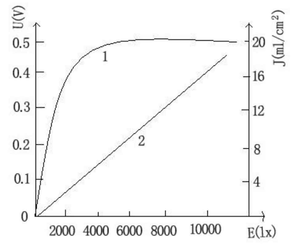
Under different light irradiation, the characteristics produced by photocells are different. Figure 1 shows the photoelectric characteristics of a silicon photocell. Curve 1 represents the characteristic curve of voltage in an open circuit when the load resistance is infinite, while curve 2 represents the short-circuit current characteristic curve when the internal resistance of the photocell is much greater than the external resistance. Thus, we can understand that the relationship between open circuit voltage and illumination is nonlinear. When reaching a certain illumination intensity, it tends to become saturated. When the circuit tends to short-circuit, the current has a linear relationship with illumination within a certain illumination range, and the greater the degree, the clearer the relationship. Therefore, when detecting continuously changing illuminance, we should reduce the load resistance to the maximum extent, allowing the photocell to operate in a short circuit state, which can also be seen as using the photocell as a current source. Photocells can also be used as voltage sources when the optical signal continuously changes.
2.3.3 Temperature characteristics
The open circuit voltage and short circuit current of photocells also change with temperature, which is called the temperature characteristic of photocells. Because it can cause errors in measurement or control accuracy related to the performance of photovoltaic devices, one of the important properties of photovoltaic cells is temperature characteristics. The higher the temperature, the lower the open circuit voltage of the silicon photocell. The short-circuit current is not significantly affected by temperature. Therefore, when using photocells in the manufacturing of detection components, it is necessary to consider the errors caused by temperature and take corresponding measures.
2.3.4 Frequency characteristics
Photocells require a certain amount of time to generate and recombine electron hole pairs when exposed to light, and the speed of generation and recombination is influenced by the intensity of light. The amplitude of the change in the output current of the photocell will decrease as the modulation frequency increases. Due to the good characteristics and high operating frequency of silicon photocells, we choose silicon photocells with smaller load resistance and smaller area for work that requires high modulation frequency to reduce the time difference between the generation and recombination of electron hole pairs and improve frequency characteristics.
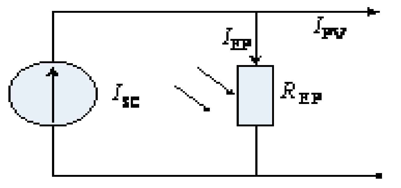
2.4 Analysis of photovoltaic array model
The mathematical model of the photovoltaic array shown in Figure 2 is composed of a grid connected circuit with a constant current source and a variable resistor. The basic idea of our design is based on the mathematical model of this photovoltaic array.
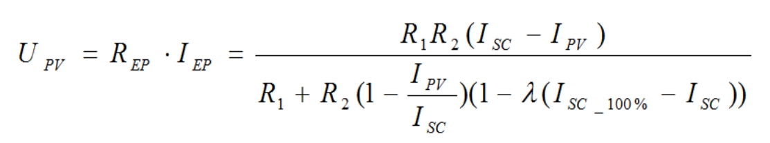
When temperature is not considered, the resistance REP can be equivalent to a function of light intensity and load current, as shown in the formula:
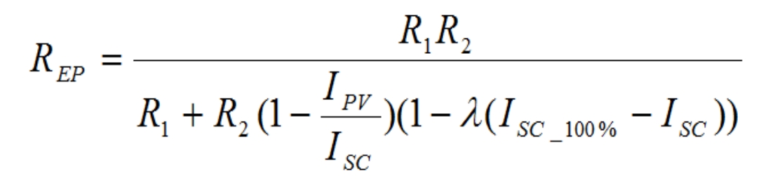
The resistance values of R1 and R2 in the formula are constant, Isc-100% is the short-circuit current under infinite light intensity, ISC is the short-circuit current value generated in actual conditions, and IPV represents the load current. Then:
3. Design of photovoltaic grid connected inverters
3.1 Design advantages of DSP based control systems
Compared to traditional inverter systems, we use ferrite cores to reduce core losses. At the same time, its low conductivity requirement also reduces copper loss, and increasing the circuit voltage for high-frequency operation also reduces switching loss, so the system has the advantage of high efficiency. In addition, there are advantages such as low harmonic distortion, high reliability, light weight, and the ability to provide direct interface with the power grid. I won’t introduce it one by one here.
3.1.1 Description of DSP Technology
A digital signal processor is a DSP. Its internal structure adopts a wide range of pipeline operations that separate program and data, with specialized hardware multipliers that can quickly complete various digital signal processing algorithms. It is to receive an analog signal and convert it into a digital signal of 0 or 1, process the signal accordingly, and then interpret the digital data back into analog data or actual environmental format in other systems. Its two characteristics are strong processing power and high-speed operation ability.
3.1.2 Characteristics of DSP chips
DSP chips are mainly used in implementing various digital signal processing algorithms, with the following characteristics: they can perform multiple operations simultaneously;
Can overlap operations such as finger retrieval, decoding, and execution;
Can complete both multiplication and addition simultaneously within one cycle;
Due to having RAM, two blocks can be accessed simultaneously through independent data buses, and so on.
Due to these advantages, it is very suitable for use in microprocessors for digital signal processing operations.
3.2 Basic circuit of inverter
Inversion and rectification are relative. As most of our electrical needs are AC power, they cannot be directly powered by DC power sources (such as photocells, dry batteries, etc.). If we want to use the electricity from DC power sources, we need to convert DC power into AC power. At this point, we need to connect an inverter conversion device to provide electricity to the load. The induction heating power supply and uninterruptible power supply we use are all manufactured with inverters as the core.
As shown in Figure 3: Single-phase bridge inverter circuit.
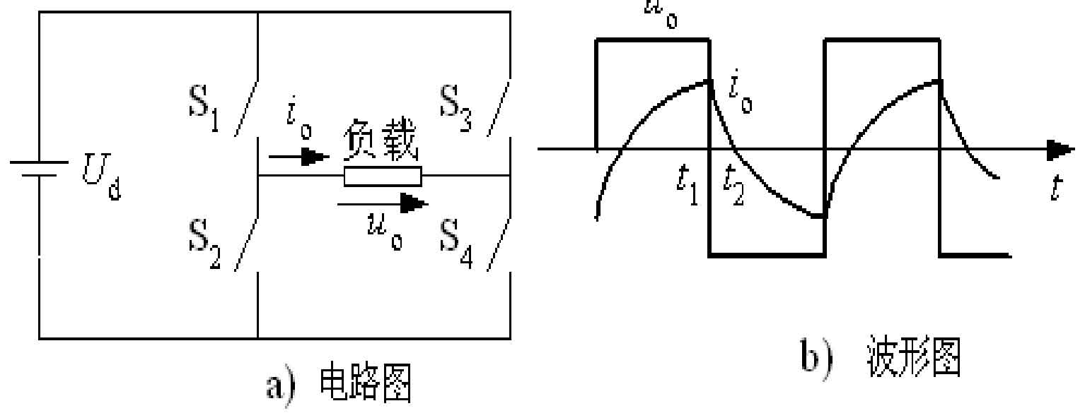
From the figure, we can understand that when a positive load voltage is required, S1 and S4 can be closed, S2 and S3 can be opened. When a negative load voltage is required, switches S1 and S4 can be opened, and switches S2 and S3 can be closed to achieve DC to AC conversion. By changing the speed of opening and closing two sets of switches, the output AC frequency can be different. When carrying a resistive load, the waveform of the load current is the same, and the phase is also the same. When carrying an inductive load, the hysteresis and waveform are also different, as shown in Figure 3 (b).
As shown in Figure 3 (b), before time t1, i0 and u0 are both positive; T2 is disconnected at all times, and u0 becomes negative, but cannot immediately reverse. It flows out from the negative pole of the power supply, flows through the load to the positive pole, and slowly feeds back to the power supply, gradually decreasing. After a period of time, it decreases to zero, and then gradually increases in reverse direction. Commutation is the process of transferring current from one branch to another, also known as commutation. There are four ways:
(1) The process of achieving commutation through the self closing ability of fully controlled devices is called device commutation.
(2) The method of providing commutation voltage through the power grid is called grid commutation. For example, controllable rectifier circuits and AC voltage regulating circuits do not require additional commutation components or components with turn-off capability.
(3) The commutation method of providing commutation voltage through the load is called load commutation.
(4) The method of applying reverse voltage or reverse current to the thyristor to be turned off by setting an additional commutation circuit is called forced commutation. It can also be called capacitor commutation because it is achieved by utilizing the energy stored on the additional capacitor.
3.3 Voltage source inverter circuit
The voltage source inverter circuit is shown in Figure 4
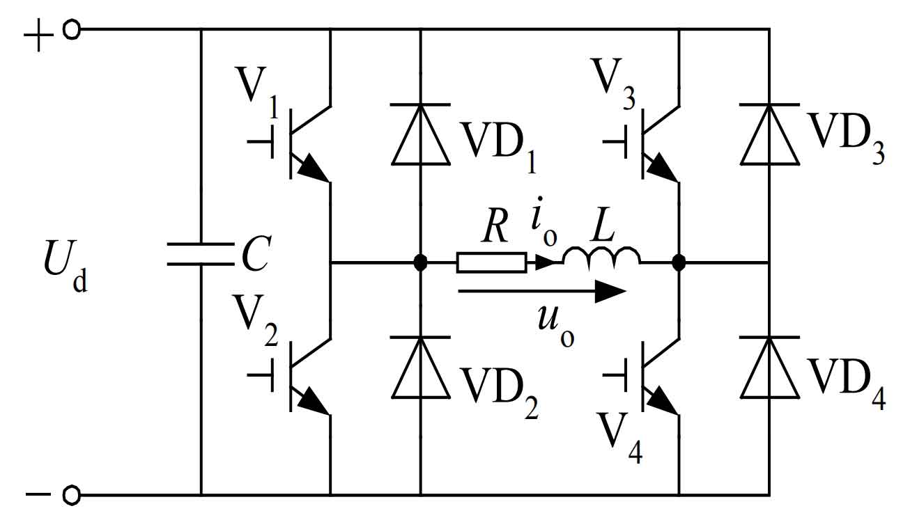
The characteristics are as follows:
(1) The DC side is a parallel large capacitor or voltage source, and the DC voltage is basically non pulsating.
(2) The output current varies with different load impedances, and the output voltage presents a rectangular waveform.
4. Summary
This design mainly uses a digital signal processor to achieve the inverter and grid connection of solar photovoltaic arrays. The main analysis introduces the photovoltaic array, the system diagram and functions of the main components, the maximum power tracking method, and the powerful control functions of many control chips. This article utilizes the MPPT control method to track the maximum power point of photovoltaic cells, which improves the efficiency of the system. By adopting digital SPW control, automatic grid connection is achieved, reducing harmonic interference, and efficiently converting direct current generated by solar photovoltaic cells into 50HZ sinusoidal alternating current for use in the power grid.
Due to my limited knowledge and experience in photovoltaic grid connection control, as well as insufficient theoretical support, there are still shortcomings in this design that need to be gradually accumulated and improved in my future work and life. In short, through the design of this photovoltaic grid connected inverter, I have gained a deeper understanding of device characteristics, circuit expansion, and other aspects during this process. This will be a huge wealth for me in my future work and life.