
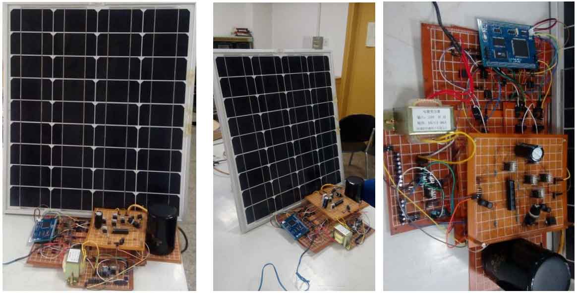
A physical prototype has been produced, and the physical image is shown in Figure 1. To verify the correctness of this design, some indicators and performance of the physical object have been tested and analyzed below.
1. Performance testing of auxiliary power supply
The auxiliary power supply is responsible for supplying power to important parts such as DSP2812, driving circuit, sampling circuit, etc. The correctness and stability of its output will directly affect the stability of the entire system, which is the foundation of the entire system. Therefore, this article first tests and analyzes the auxiliary power supply part. The main tool used for testing the auxiliary power supply is a multimeter. The specific testing process and results are shown in Figure 2.
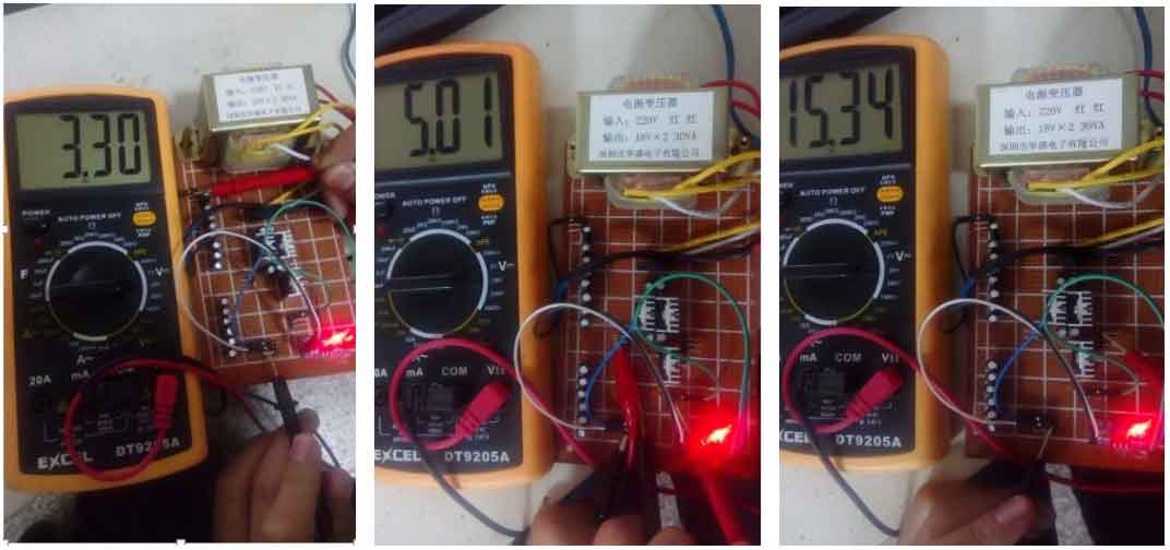
Result analysis: As shown in the above figure, the output results of 3.3V, 5V, and 15V were measured using a multimeter. The 3.3V output is used to power the main control chip, which requires high stability. The test results prove that the output data is correct, without any deviation, and meets the design requirements. The 5V output is mainly used for IGBT drive circuits. The test results show that the data is very stable, with a deviation of 0.01V, but the deviation value meets the design requirements within the allowable range. The 15V voltage output is mainly used for amplifier power supply in sampling circuits. The test results are stable, but there is a deviation of 0.34V, which is within the allowable range. Therefore, the 15V power supply meets the design requirements.
2. PWM testing in boost circuits
The correctness of PWM in the boost circuit is the key to determining the success or failure of DC-DC boost and maximum power point tracking. Therefore, the PWM in the boost circuit was tested next. Test tool oscilloscope, test results and analysis are shown in Figure 3.
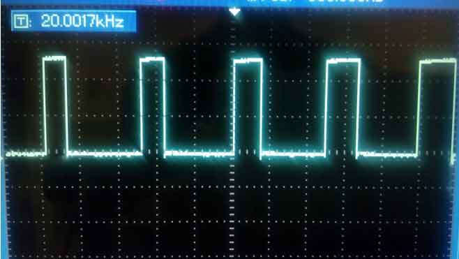
According to the oscilloscope test results, the PWM waveform frequency is 20.0017KHz, which has a deviation of 0.0017Hz from the set 20KHz. This deviation is very small and can be ignored, so the waveform frequency meets the design requirements. Due to being in the process of maximum point tracking during testing, the duty cycle is constantly changing. From the graph, it can be seen that the duty cycle is gradually increasing, indicating that the solar energy transmission voltage is being adjusted in the direction of decreasing. The initial Vmax set during testing is greater than the current maximum power point voltage, so the adjustment direction should be towards the direction of voltage reduction, consistent with the display on the graph, indicating that the PWM output is normal.
3. SPWM waveform testing
SPWM waves are mainly used to control the on/off of IGBT tubes in inverter circuits, and are the basis for phase and frequency modulation. The tool used for testing it is an oscilloscope, and the test results are shown in Figure 4.
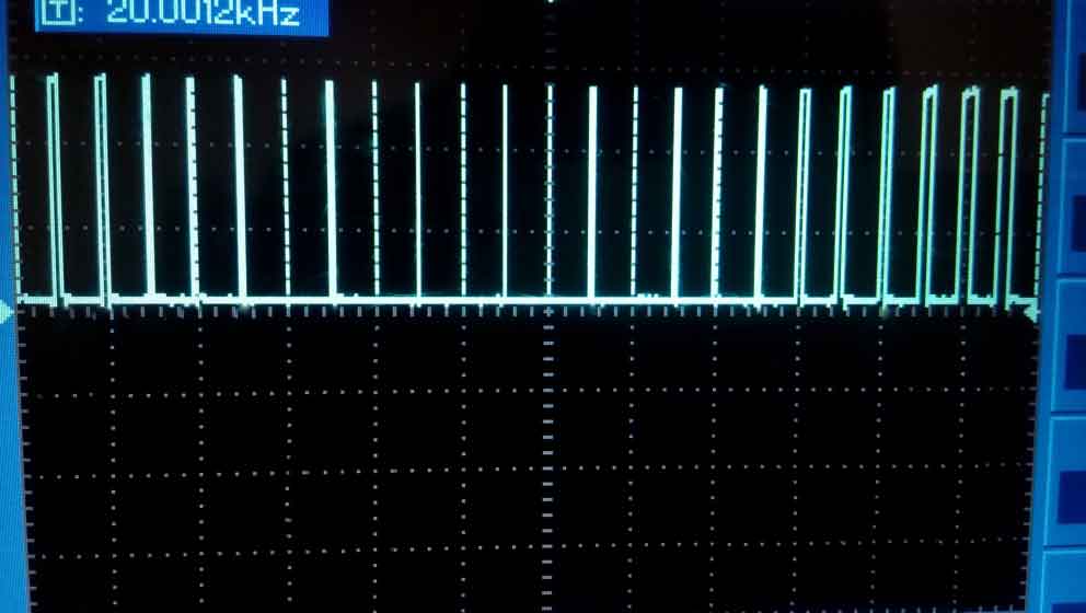
According to the oscilloscope test results, the SPWM waveform frequency is 20.0012KHz, which has a deviation of 0.0012Hz from the set 20KHz. This deviation is small and can be ignored, so the waveform frequency meets the design requirements. In this design, the SPWM wave is generated using the regular sampling method. From the image, it can be seen that its duty cycle follows the sine wave variation pattern, and the output is normal.
4. Solar inverter output current test
The testing tool for the output current of solar inverters is an oscilloscope. The test results are shown in Figure 5.
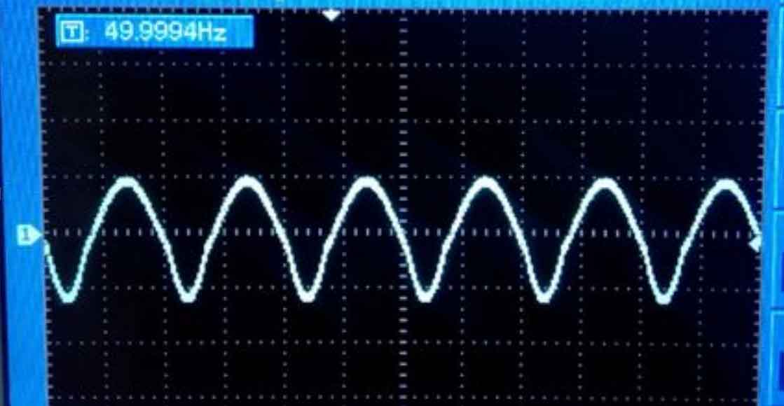
According to the oscilloscope test results, the output current of the solar inverter is a sine wave with a frequency of 49.9994Hz, which has a slight frequency deviation but meets the requirements for grid connection frequency. The waveform is slightly distorted, but within an acceptable range.
5. Prototype grid connection test
During the prototype grid connection test, both the output current of the solar inverter and the grid voltage were tested. The testing tool is an oscilloscope, and the test results are shown in Figure 6.
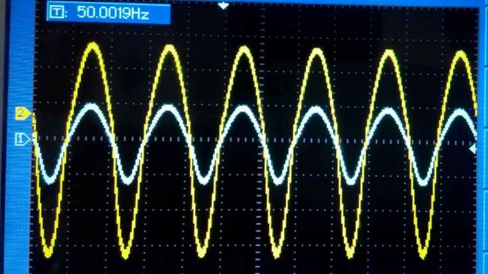
During testing, channel 1 of the oscilloscope is connected to the output current signal of the solar inverter, while channel 2 is connected to the grid voltage signal. According to the test results, it can be seen that the phase and frequency of the output current of the solar inverter and the grid voltage are basically consistent, which proves that the software and hardware design in this design is correct and feasible.
Based on a thorough analysis of the technical requirements and standards of solar grid connected inverters, this design referred to a large amount of relevant domestic and foreign materials, and completed the hardware circuit design of each component unit and the programming of each software module. Finally, a prototype was produced, and stability and reliability tests were conducted on the prototype, The following conclusion has been drawn: the system architecture of the solar photovoltaic grid connected inverter designed in this project is correct and feasible, and can achieve safe grid connection; The improvement of disturbance observation method is effective and feasible.
The research work of this article mainly includes:
- Studied the background, development status, and market prospects of solar photovoltaic grid connected inverters. Extensive research and collection of relevant technologies and principles used in the system.
- The voltage and current output characteristics of solar cells were studied, and the power output characteristics of solar cells were identified.
- The structure and inversion method of existing solar photovoltaic inverters have been studied and optimized, and the overall structure of the solar photovoltaic inverter in this design has been determined.
- Completed the hardware circuit design and hardware selection of the entire system.
- The maximum power point tracking method for solar cells was studied, and the principle of conventional disturbance observation method was analyzed in depth. The original disturbance observation method was improved three times, and the maximum power tracking algorithm in this project was designed. Finally, simulation was conducted, and the results showed that the improvement plan of this design is feasible.
- The system flowchart of this system was drawn, and the software module division and corresponding programming work were completed.
- Completed the physical production and debugging, tested and analyzed the final output waveform of the solar photovoltaic inverter, and provided the test results.