
The overall structure of the system can be roughly divided into two parts: AC and DC. Due to the presence of electromagnetic component transformers in the auxiliary power supply, and the involvement of AC power in multiple parts of the entire system, considering the interference of transformers and AC power on DC signals, it is best to use four or even six layer boards for the system circuit. However, due to limited funding, this design adopts a method of connecting multiple circuit boards and multiple circuit modules to prevent interference with DC signals. And based on this, the system architecture was designed and various functional modules were divided. It is mainly divided into auxiliary power supply, boost and inverter unit, main control unit, driving unit, sampling unit, etc. The following text will conduct functional analysis and structural selection for each module unit.
1.Common topology structures of solar photovoltaic inverter circuits
At present, there are many types of commonly used solar grid connected inverters, which are generally classified based on their internal structure: whether transformers are used in the equipment, and the operating frequency of the equipment. This article selects several solar inverters for explanation, each with its own advantages and disadvantages, as follows.
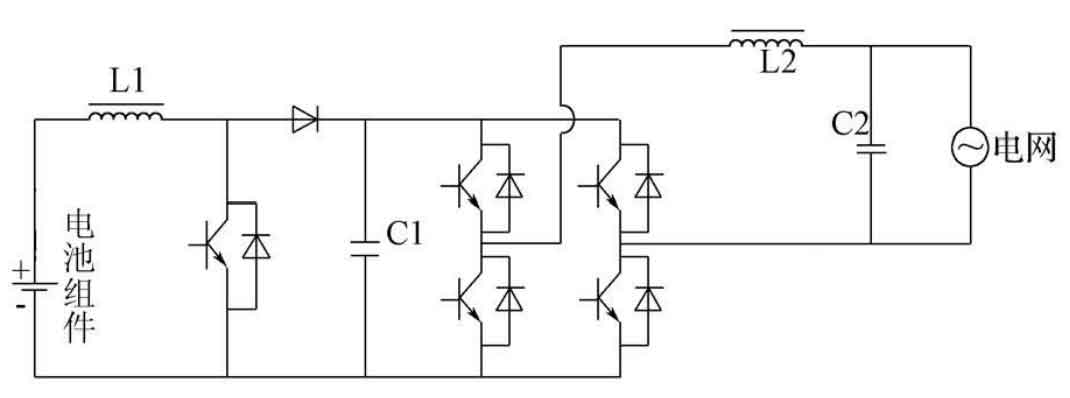
1.1 Direct inverter circuit topology
The topology of the direct inverter circuit is shown in Figure 1
Advantages:
(1) The circuit structure is simple, and due to the use of a direct solar inverter for the power transformer, the bulky transformer part can be saved, and the conversion efficiency can reach 99%.
(2) Lightweight and cost-effective.
Disadvantages:
(1) This circuit topology has no electrical isolation between the input and output terminals, resulting in the photovoltaic cell being inevitably connected to the power supply system when grounded, which poses a serious safety hazard.
(2) Due to the absence of an internal isolation transformer, the DC component on the input side can easily enter the AC power grid at the output end, causing adverse effects on the power grid.
(3) The input voltage of this circuit topology inverter circuit should be at least 350 V or above, and the electrical insulation of the photovoltaic panel should not be low, otherwise it will cause ground leakage.
1.2 Power frequency isolation circuit topology
The topology of the power frequency isolation circuit is shown in Figure 2
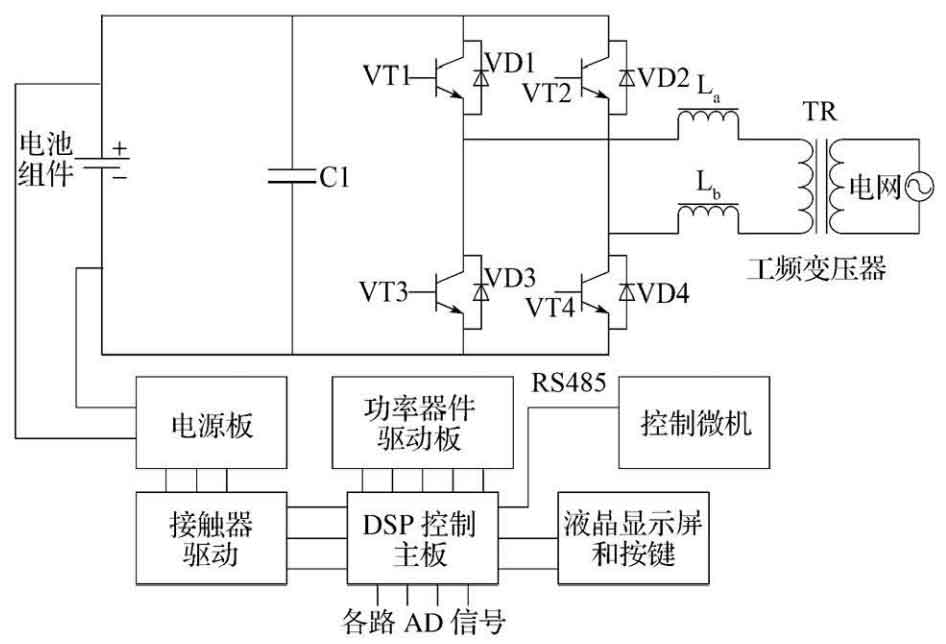
Advantages:
(1) The high-frequency transformer used for electrical isolation in this circuit topology has good safety performance, high overall system reliability, and good impact resistance.
(2) This circuit topology can be directly grounded.
Disadvantages:
(1) Due to the increased transformer losses in this topology, the system efficiency is relatively reduced.
(2) The topology itself has added bulky power frequency transformers, which will greatly increase design costs, overall weight, and installation space.
1.3 High frequency isolation circuit topology
The topology of the high-frequency isolation circuit is shown in Figure 3.
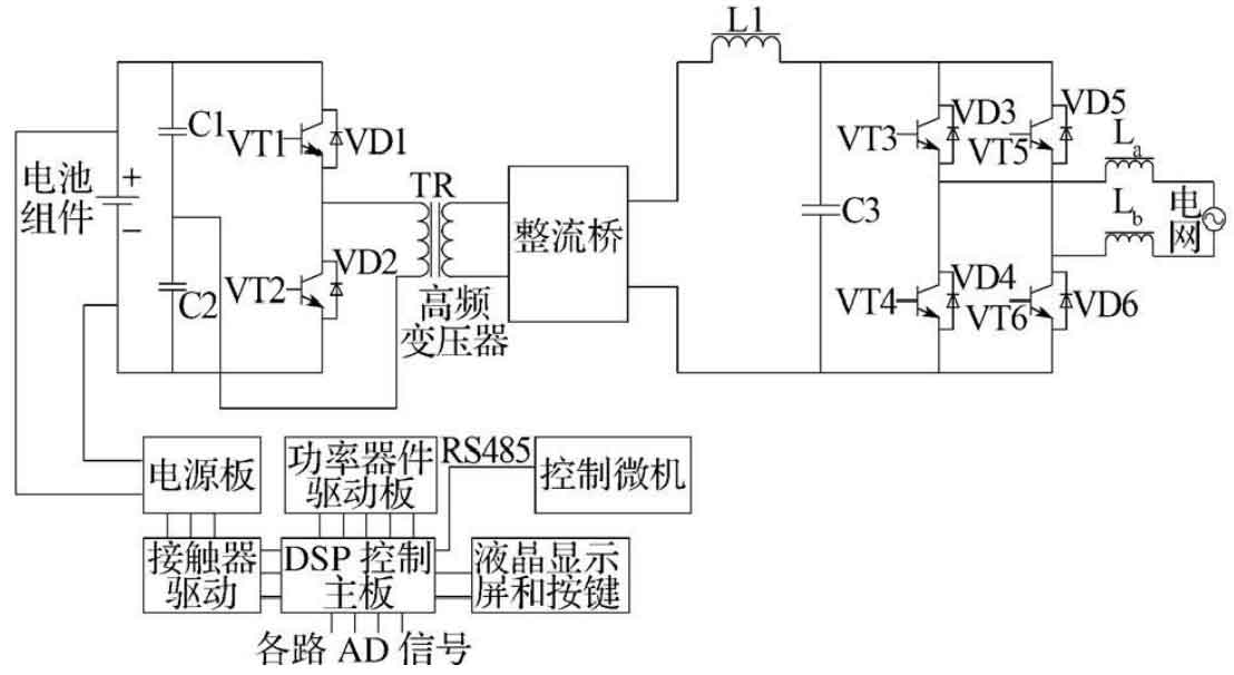
Advantages:
(1) Compared with the power frequency isolation topology, the volume and weight of the isolation transformer in the system can be greatly reduced due to the use of high-frequency switching signals.
(2) This topology has the dual advantages of electrical isolation and lightweight.
Disadvantages:
(1) High frequency transformers inevitably generate large amounts of heat, leading to severe heat dissipation problems. This makes solar inverters with this structure generally have lower power levels, so this circuit type is generally used in equipment below 5 kilowatts.
(2) The high-frequency DC/AC inverter operates at a high frequency, which makes it difficult to handle harmonics in high-order power sources.
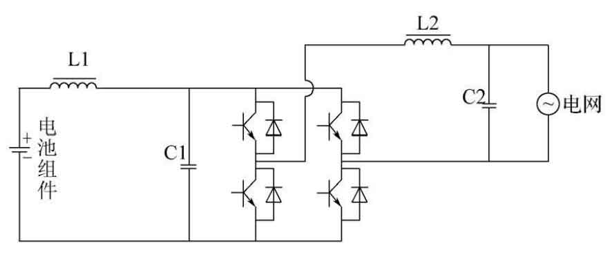
1.4 High frequency boost non isolated circuit topology
The topology of the high-frequency boost non isolated circuit is shown in Figure 4
Advantages:
(1) The topology of the high-frequency boost non isolated circuit is similar to the structure of the direct inverter circuit, no longer using a power frequency transformer, resulting in a reduction in system weight and a significant improvement in efficiency. At the same time, adding a Boost boost circuit is beneficial for improving and controlling the input voltage on the DC side, so that the output voltage width of the front-end photovoltaic components of the system can reach 150-450 V.
(2) This type of circuit has outstanding advantages when used in micro and single-phase grid connected equipment, and is suitable for systems where the output voltage of photovoltaic modules is not very high. Photovoltaic grid connected equipment designed with this type of circuit has basically become the mainstream in the small and single-phase grid connected equipment market in Europe and America.
Disadvantages:
(1) The high-frequency boost non isolated circuit topology is the same as the direct inverter topology. Due to the lack of electrical isolation within the system, the AC and DC power sources are grounded, which is detrimental to the insulation, grounding, and personnel safety of the system.
After comparing and analyzing the advantages and disadvantages of various topologies, this design ultimately chose a high-frequency boost non isolated circuit structure.
2. System architecture and operating principles
The solar inverter designed in this project mainly consists of auxiliary power supply, main control unit, boost and inverter unit, driving unit, and sampling unit. Its structural diagram is shown in Figure 5. Among them, the auxiliary power supply is mainly used to provide driving power to the main control unit and other DC components. The main control unit is composed of the DSP2812 chip and its peripheral circuits, and is the central control center of the entire design. The boost and inverter unit consists of a DC/DC boost circuit (which boosts the voltage obtained through the solar array) and a DC/AC full bridge inverter circuit (which inverts the results obtained through the Boost circuit), used to process the direct current obtained through the solar module. The driving unit is mainly the IGBT driving circuit, used to drive the IGBT. The sampling circuit mainly consists of a solar cell voltage and current sampling circuit, a grid connected current sampling circuit, and a grid voltage sampling circuit. It is mainly used to sample the voltage and current in each stage of the system and provide the sampling signal to the core control unit.
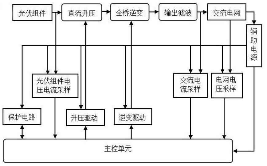
System workflow: After the system is powered on, the system is first initialized. After initialization, the system starts running. The electrical energy obtained through solar cell modules is filtered and processed, and then transmitted to the front-end boost module. The sampling unit collects voltage and current data from filtered DC power and transmits the obtained data to the main control unit. After processing, the main control unit generates corresponding PWM waves and transmits them to the DC boost IGBT drive circuit. The IGBT drive circuit drives the DC-DC boost circuit to boost the filtered DC power to 400V and transmit it to the subsequent inverter circuit. After relevant calculations, the main control unit outputs the corresponding PWM wave, which is transmitted to the corresponding switch driver circuit in the full bridge inverter. The switch driver circuit drives the subsequent inverter module to convert DC power into 220V AC power. Filter the electrical energy obtained from the solar inverter. At the same time, the sampling unit will collect data on AC current and grid voltage and transmit the obtained data to the main control unit. After processing, the main control unit will adjust the output PWM wave as needed to adjust the frequency and phase of the final grid connected AC power to be in the same frequency and phase as the grid.
3. Main control unit
The control chip used in the main control unit in this design is the DSP2000 series microcontroller. Among them, the main chip adopts STMDSPF2812 chip. DSP, also known as Digital Signal Processor, is the theory and skill of applying numerical calculations to process signals. Of course, DSP can also be seen as an application skill, called DSP technology and application, which is also an emerging discipline. This discipline is related to many other disciplines and has a wide range of applications.
3.1 TMS320F2812 related parameters and functions
(1) Select high-performance static COMS technology;
(2) Support JTAG boundary scanning interface;
(3) High performance 32-bit CPU with Harvard bus architecture, supporting 16 × 16 bit and 32 bit × 32-bit multiplication, addition, and double multiplication operations are also supported × 32-bit double multiplication operation; Having fast interrupt response and interrupt handling skills; Unified storage design approach; 4MB program/data addressing space; Efficient code conversion function (supports C/C++and assembly;
(4) On chip storage space, with 128K × 16b on-chip Flash; ROM space: 128K × ROM of 16; 1K × 16b OTP ROM with 4K read-only memory × 16 bit
(5) Boot mode with software startup included;
(6) Standard mathematical function library;
(7) External memory interface, up to 1M × 16b of total storage space;
(8) Three external interrupts, External Interrupt Extension (PE) module, capable of supporting 96 external interrupts, currently only 45 external interrupts are used;
(9) 3 32-bit CPU timers for controlling peripheral devices of the motor;
(10) Two event managers;
(11) Serial peripheral devices, serial peripheral interfaces (SPI); Two channel serial communication interface (SCI), standard SCI port; Enhanced CAN module (eCAN); Multi channel buffered serial interface (McBSP) and serial peripheral interface mode;
(12) . 12 bit ADC conversion module, 2 × 8-channel input channel; Single or cascading conversion methods; The maximum conversion rate is 80ns/12.5Msps;
(13) Up to 56 independent programmable, general-purpose input/output (GPIO) pins;
(14) Advanced simulation mode, capable of real-time analysis and breakpoint setting, and supporting hardware simulation;
(15) Development tools, DSP integrated systems, JTAG simulators;
(16) Low power consumption mode and energy-saving mode, supporting three modes: idle, wait, and suspend; Static/enable independent peripheral clock;
(17) Working temperature, A: -40~85 ℃ (GHH, ZHH, PGF, PBK), S: -40~125 ℃ (GHH, ZHH, PGF, PBK), Q: -40~125 ℃ (PGF, PBK);
4. Boost and inverter unit
Based on the characteristics of large output voltage oscillation in photovoltaic power generation systems, multiple schemes were compared and demonstrated, and finally, a two-stage structure without a transformer was selected as the main structure of this design. The two-stage structure consists of a front-end DC/DC boost converter and a back-end DC/AC solar inverter, which will be connected through Dclink. There are three main types of topology structures for DC/DC converters, namely buck, boost, and boost buck. The DC/DC circuit can change the impedance R of the solar cell power supply circuit, thereby achieving impedance matching. Considering the actual situation, we have decided to adopt a boost topology structure based on the characteristics of solar cells. The main advantage of Boost boost converter is its high efficiency. We can control the change in duty cycle to control the change in energy transfer efficiency. However, the disadvantage of the Boost circuit is that it can cause significant losses to the circuit, as its input voltage is lower and the input current is higher at the same power. But the Boost circuit has unique advantages and is suitable for solar cell power supply. The DC high voltage used for inversion will be converted by the lower solar cell voltage, which is still a good solution. It can control the voltage oscillation of a photovoltaic power generation system to stabilize it within an appropriate voltage range, while tracking the maximum power point, in order to increase the economic performance of the photovoltaic system and reduce the system’s power generation cost [20]. In this design, the rated voltage output by the photovoltaic array is between DC60V-DC140V, and the electrical energy is converted into DC power of Dclink through a Boost converter. In this design, a single-phase full bridge inverter circuit is used for the DC to AC inverter section of the later stage. Its function is to invert the DC power of Dclink and convert it into sinusoidal AC power through rectification and filtering.
In this design, a full bridge inverter is used to complete the inverter process from DC to AC. The main principle of this form is to perform low-frequency commutation on the high-voltage side IGBT and high-frequency sine pulse width modulation on the corresponding low-voltage side IGBT. Figure 6 shows a typical driving mode diagram.
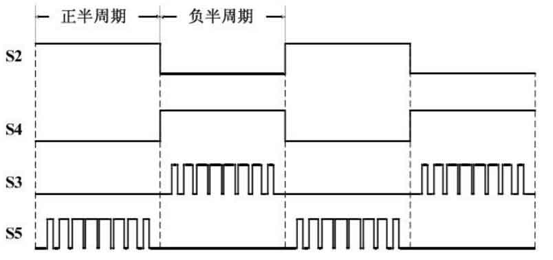
When S5 is undergoing pulse width modulation, S2 maintains a positive half cycle operation. S4 and S3 remain turned off during the positive half cycle. At the negative half cycle, when S3 performs pulse width modulation, S4 remains in the on state. S2 and S5 will turn off in the negative half cycle. The AC sine voltage waveform can be obtained by outputting the LCL filter. The high-frequency control signal adopts a sine modulation pulse width of 20kHz, and the low-frequency control signal is the grid frequency collected through the real-time detection circuit module of the grid voltage, achieving the output sine wave to be consistent with the frequency and phase of the grid.
This transformation technique has the following advantages:
(1) The current will not flow freely on the high-voltage side of the reverse diode, thus minimizing unnecessary losses;
(2) The low-voltage side IGBT will only switch at 50Hz power frequency, mainly due to conduction loss;
(3) Due to the fact that IGBTs on the same phase will never be converted in a complementary manner, it is impossible for bus short circuit breakdown to occur.
5. Driver unit
In this design, there are 5 IGBT tubes, which are the key to determining the success and compliance of boost and inverter. To control these switching tubes, the correct driving circuit needs to be equipped. The function of the driving circuit is to perform a series of corresponding processing on the PWM wave output by the DSP, in order to drive the switching device on a safe basis. For high-power IGBT, the selection of driving circuit is based on the following parameter requirements: device turn off bias, gate charge, stability, and power supply condition. Due to the switching characteristics and safe working area of IGBT changing with the gate drive circuit, the performance of the drive circuit will directly affect the normal operation of IGBT. To ensure the reliable operation of IGBT, IGBT has put forward the following requirements for its driving circuit.
(1) Provide appropriate forward gate voltage to IGBT. And after the IGBT conducts, the gate drive circuit should provide sufficient amplitude of driving voltage and current to the IGBT, so that the power output stage of the IGBT is always in a saturated state. When subjected to instantaneous overload, the driving power provided by the gate drive circuit should be sufficient to ensure that the IGBT does not exit the saturation zone.
(2) Can provide sufficient reverse gate voltage to IGBT. During the IGBT shutdown period, due to the operation of other parts of the circuit, some high-frequency oscillation signals will be generated in the gate circuit. These signals can cause the IGBT that should have been cut off to be in a micro pass state, increasing the power consumption of the transistor. This will put the voltage regulating circuit in a short-circuit through state. Therefore, it is best to apply a reverse gate voltage to the IGBT in the cut-off state, so that the IGBT can still reliably cut off even when there is switch noise in the gate.
(3) Equipped with gate voltage limiting circuit to protect the gate from breakdown. The limit voltage of the IGBT gate is generally+20 V, and if the driving signal exceeds this range, it may damage the gate.
(4) Due to the fact that IGBTs are mostly used in high-voltage situations. Sufficient input and output electrical isolation capability is required. So the driving circuit should be strictly isolated from the entire control circuit at the potential, generally using high-speed optical coupling isolation or transformer coupling isolation.
(5) The gate drive circuit of IGBT should be as simple and practical as possible. It should have the complete protection function of IGBT, strong anti-interference ability, and the output impedance should be as low as possible.
The core chip selected for this design’s driver circuit is the IR2110 dedicated driver chip, and based on this, the driver circuit is designed.
6. Sampling unit
This article requires sampling two AC signals and two DC electrical signals. Among them, the two AC signals that need to be sampled are the output current sampling of the solar inverter and the grid voltage sampling; The two DC signals that need to be sampled are the output voltage signal of the solar cell and the output current signal of the solar cell. Therefore, four sampling circuits need to be designed in this design. And the collection of these signals requires the use of sensors, and Hall sensors are used in this design. Merely using Hall sensors to complete the sampling unit is not enough. Due to the input voltage of the DSP2812 chip being 0-3.3V, it is necessary to design a signal conditioning circuit to process the sampled signal through a series of processes such as level transformation and filtering, so that the signal detected by the sensor is within the receiving range of the ADC module.