
The off-grid solar inverter designed is mainly for use in households without electricity.Table 1 shows the statistics of household electricity load in areas without electricity.According to the statistics, the maximum power consumption in summer is when using a refrigerator, and the system needs to provide a maximum output power of 437W. The average daily electricity consumption of a household is 1618kWh. In the western region, there is less continuous rainy weather, and considering that the battery can supply power for 3 days of rainy weather, the battery capacity is at least 4854kWh.
| Number | Load Name | Load power | Daily working hours (h) | Daily power consumption (Wh) |
| 1 | 17-21 inch LCD color TV | 45W | 6 | 270 |
| 2 | Satellite receiver | 15W | 6 | 90 |
| 3 | Shadow recording or recording machine | 20W | 2 | 4 |
| 4 | 3 LED lights | 9W | 4 | 108 |
| 5 | Blower | 20W | 3 | 60 |
| 6 | Double drum washing machine | 120W | 0.5 | 60 |
| 7 | Laptop (or tablet) | 40W | 3 | 120 |
| 8 | 180 liter refrigerator | 140W | Daily power consumption of 0.86kWh | 860 (for summer use) |
| 9 | Other appliances (such as mobile phone charging, etc.) | 10W | 1 | 10 |
| Total | 437W | 1618kWh |
According to the above requirements, the main parameters of the off-grid solar inverter designed in this article are:
(1) Solar inverter output rated power 500W, maximum overload 10%;
(2) The solar cell is composed of two 260W single crystal silicon solar cells in parallel, with an open circuit voltage of 48V and an optimal operating voltage of 36V;
(3) Two 24V150AH gel maintenance-free lead-acid batteries are used in parallel for energy storage, with a capacity of 7200kWh, meeting the design requirements and leaving a certain margin.
1. System composition
Figure 1 is the system structure diagram of the off-grid solar inverter designed in this article, including: DC output of PV panel, battery charging circuit, DC/AC conversion circuit, output filtering boost circuit, digital controller DSP and its peripheral circuit.The peripheral circuit includes drive circuit (including battery charging circuit drive, DC/AC conversion circuit drive), voltage, current, temperature sampling circuit, output voltage, current sampling circuit, protection circuit, alarm circuit.The modules of the system are relatively independent and easy to control, which can achieve modular design of system software and hardware. The system adopts the method of inverting first and boosting later, which ensures that there is no high voltage before the primary side of the transformer, and the voltage withstand requirements of the device are low. Touching the main control board by human body will not cause electric shock, which greatly improves the safety of the system.
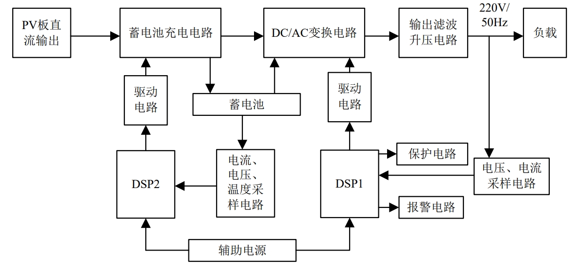
Introduction to main circuit functions:
(1) Battery charging circuit: This part of the circuit mainly implements two functions: first, it controls the charging of the battery to achieve optimal charging;second, it implements maximum power tracking of the solar panel.
(2) DC/AC conversion circuit: It converts the DC power provided by the battery charging circuit and battery into 50Hz AC power.
(3) Output filter circuit: Filter out high-order harmonics through an LC low-pass filter, and boost the voltage to 220V using a power frequency transformer.
(4) Drive circuit: Amplify the control signal sent by the DSP to ensure that the switch tube can work reliably.
(5) Detection circuit: sampling the required feedback signal and converting it into the digital signal required by the DSP.
(6) Protection circuit: protects the system against excessive current, high voltage, high temperature, and short circuit.
The use of a power frequency transformer to boost the 50Hz output low voltage generated by the solar inverter to 220V makes the power of the 500W power frequency solar inverter less significant compared to the lead-acid battery in the system.In this process, the maximum power tracking of the solar panel and the optimal charging of the battery are achieved. The battery’s rear-stage circuit is a full-bridge conversion circuit that converts DC power into 50Hz AC power, which is then outputted as high-quality 220V/50Hz voltage through a power frequency transformer and LC low-pass filter circuit.
2. Introduction to solar cells
As the energy source of photovoltaic power generation, solar cells are an essential component of the entire photovoltaic power generation system.Solar panels are combined in series and parallel to form solar cell modules.
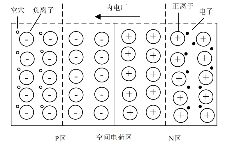
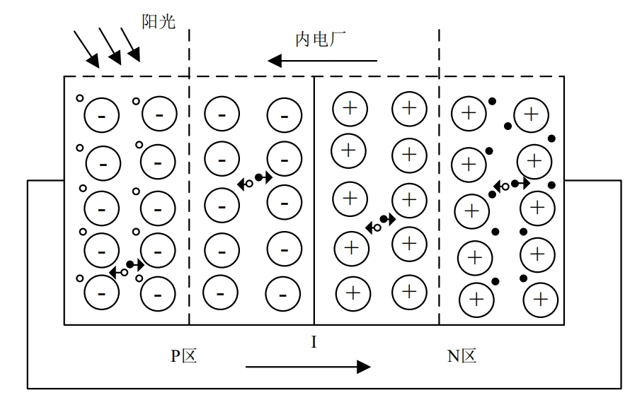
French scientist A. E. Becquerel discovered the “Photovoltaic Effect” in 1839. The principle of this effect is that when light shines on the surface of a solar cell panel, due to the fact that the surface of the solar cell is composed of N-type and P-type semiconductors, a special film is formed at the contact surface. Under the action of light, electrons flow between the N-type region and the P-type region, reducing the concentration difference between electrons and holes in the two regions.With the continuous illumination, the concentration difference between the two regions continues to increase, so when there is a short circuit between the P region and the N region, a current will be formed.The principle is shown in Figure 2 and Figure 3:
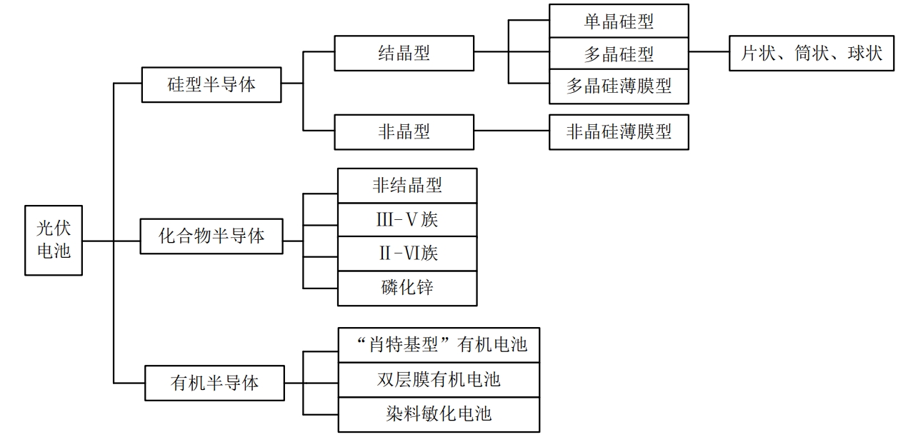
2.1 Classification of solar panels
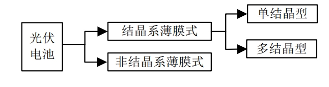
There are many types of solar panels, and Figure 4 and Figure 5 classify them from two perspectives:
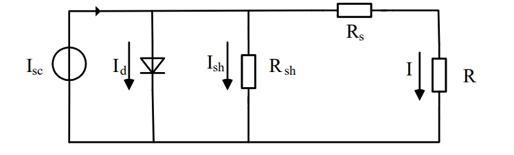
2.2 Equivalent circuit of solar cell
Figure 6 shows the equivalent circuit of a solar panel:
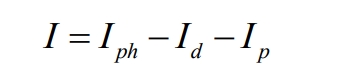
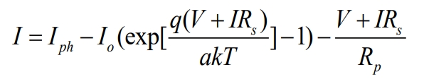
According to the current and voltage marked in Figure 6, the following formula can be derived from the circuit principle:
Among them:
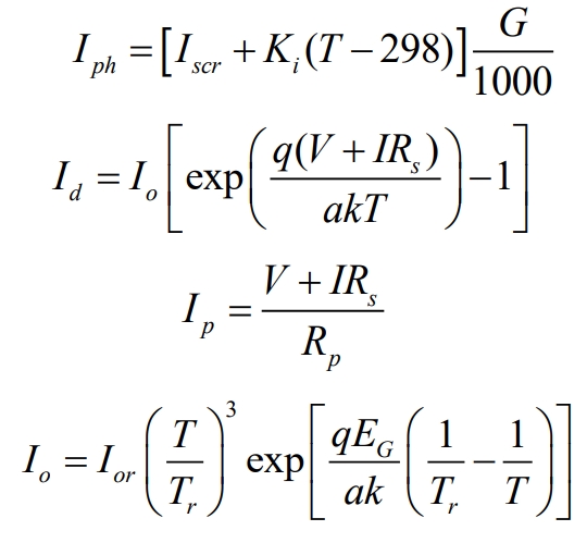
By consolidating equations 1 through 5, the output of a solar cell can be represented by equation 6:
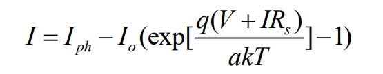
When the light intensity is high, the value of V+IRs/Rsh can be neglected, so Equation 6 can be simplified to:
Among them,
I[A]-output current of photovoltaic cell;
V[V]-port voltage of photovoltaic cell;
T[K]-the operating temperature of the photovoltaic cell;
G[W/m2]-light intensity;
Iph[A]-photo-generated current;
Io[A] – reverse saturation current of diode PN junction;
Iscr[A] – short circuit current under standard test conditions (G=1kW/m2, T=25℃);
Rs[ Ω]- equivalent resistance in series, with a resistance value ranging from 10-3Ωto a few ohms;
Rp[ Ω]- parallel equivalent resistance;
Ki[A/K]-temperature coefficient of short-circuit current;
Ideal factor of a-PN junction;
q-electron charge (1.6×10⁻¹⁹C);
k-Blotzman constant (1.38×10⁻²³J/K);
EG-band width.
2.3 Output characteristics of solar cells
The relationship between the output current and voltage of solar cells is affected by external environment, which can undergo significant changes, especially under the influence of light and temperature. This characteristic change is nonlinear.The following section will introduce the output characteristics of solar cells under changes in temperature and light, as well as several related parameters.
Several related parameters of solar cells:
(1) Short-circuit current Isc: The solar cell outputs current at the positive and negative poles in the case of short circuit, and the output current reaches its maximum at this time;
(2) Open-circuit voltage Uoc: When the positive and negative poles of the solar panel are disconnected, that is, when it is in no-load condition, the output voltage reaches its maximum value;
(3) Optimal output current Im: the current of the solar cell when the output power is maximum;
(4) Optimal output voltage Um: the voltage of the solar cell at the maximum output power;
(5) Optimal output power Pm: The maximum power that a solar cell can output under a certain external environment.
The relationship between the output voltage and current (I-U) and the voltage and power (P-U) of solar cells under different environmental conditions is shown in Figure 7.
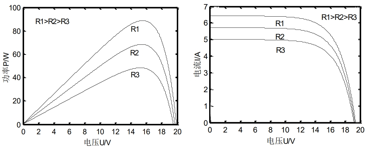
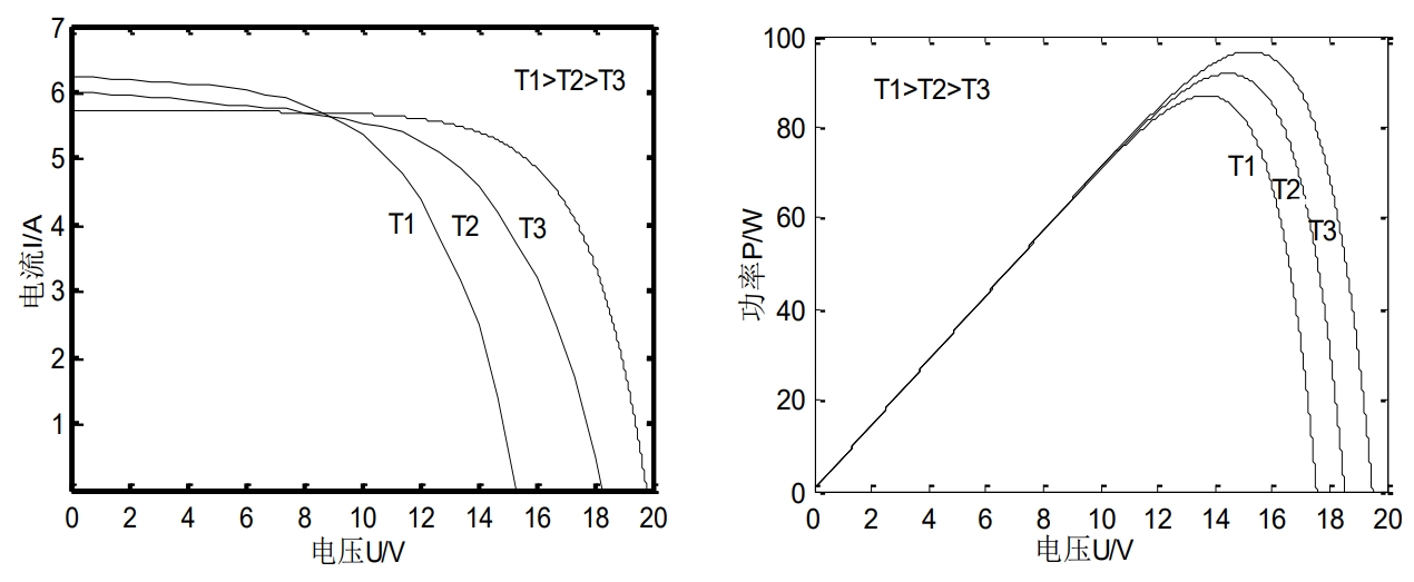
As shown in Figure 7, the main parameters of solar cell output, Isc and Uoc, will undergo regular nonlinear changes under the influence of light and temperature, and Pm will also change accordingly. However, under a certain light and temperature, this value is unique.Figure a shows the output characteristics when the ambient temperature remains constant and only the intensity of solar light changes. It can be found that only when the intensity of solar light changes, the open-circuit voltage of solar cell is basically at a constant value, with only a slight increase, but the short-circuit current varies greatly. The stronger the light, the larger the current, so the output power also increases accordingly.Figure b shows the output characteristics when the intensity of solar light remains constant and only the ambient temperature changes. It can be found that only when the ambient temperature changes, the short-circuit current of solar cell remains basically unchanged, with only a slight increase, but its open-circuit voltage decreases significantly, resulting in a corresponding decrease in output power.
3. Introduction to lead-acid batteries
Since the first lead-acid battery was invented by Frenchman Plante, it has developed for about a century and a half. The lead-acid battery initially invented did not receive large-scale use due to its low energy density, short service life, and small battery capacity.Until the beginning of the last century, with the development of the automotive industry and the urgency of people’s demand for batteries, the rapid development of lead-acid batteries was driven.Lead-acid batteries have many advantages, such as low manufacturing price and common and readily available manufacturing materials, and are widely applied in various aspects requiring batteries.
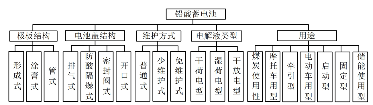
3.1 Classification of lead-acid batteries
Lead-acid batteries are classified according to different standards. Figure 8 shows the detailed classification of lead-acid batteries:
3.2 Operating principle of lead-acid battery
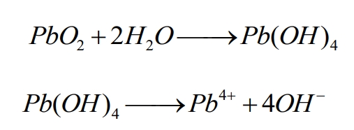
The essence of battery charging and discharging is an electrochemical reaction process in which electrical energy and chemical energy are converted into each other. Lead-acid batteries use sulfuric acid solution as the electrolyte. There are two electrode plates in the electrolyte, which are respectively the positive electrode plate composed of lead dioxide and the negative electrode plate composed of lead.The positive and negative electrode plates will produce chemical reactions in the solution.After the battery is charged, when the two plates are not connected to an external circuit, the lead on the negative electrode plate will react with the sulfuric acid in the electrolyte to generate lead ions with a positive valence of two, which will react with sulfate to generate lead sulfate and attach to the electrode plate. At this time, the two separated electrons will make the negative electrode plate have a negative polarity.A part of the lead dioxide on the positive electrode plate will react with water in the electrolyte to generate lead hydroxide. Due to the chemical properties of lead hydroxide, which are relatively easy to ionize, the hydroxide radicals generated will be dissolved into the electrolyte. Only the positive tetravalent lead ions remain on the positive electrode plate, leaving the positive electrode plate missing two electrons, which will form a potential difference between the two plates.
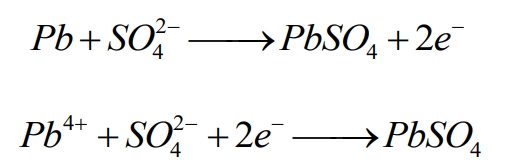
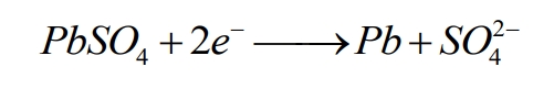
The discharge process of the battery: electrons flow from the negative plate to the positive plate, and the positive tetravalent lead ions on the positive plate become positive divalent lead ions after gaining two electrons, which react with the sulfate radicals in the electrolyte to form stable lead sulfate;The hydrogen ions ionized by sulfuric acid and the hydroxide ions ionized by lead hydroxide generate water.This process continues with the help of external circuits, forming a continuous discharge process, and its chemical reaction is:
Negative plate:
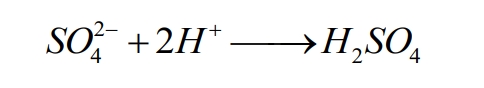
Battery charging process: Stable lead sulfate is ionized under the action of external electric energy, and the positive divalent lead ions on the positive plate release two electrons under the action of external electromotive force to become positive tetravalent lead ions, and react with oxygen ions in water to generate lead dioxide;the negative plate also gains two electrons under the action of external electromotive force to generate lead from the positive divalent lead ions, and the sulfate ions ionized from the two plates react with the hydrogen ions ionized from water to generate sulfuric acid, whose chemical reaction formula is positive plate:
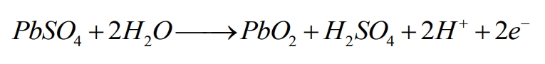
Negative plate:
Electrolyte:
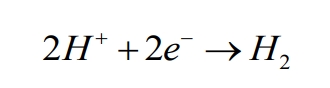
Side effects:
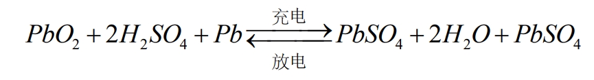
The overall reaction formula for charging and discharging is:
4. System hardware main circuit topology
Figure 9 shows the main topology of the system hardware circuit, which consists of three parts: the charging circuit, the inverter circuit, and the filtering and boosting circuit:
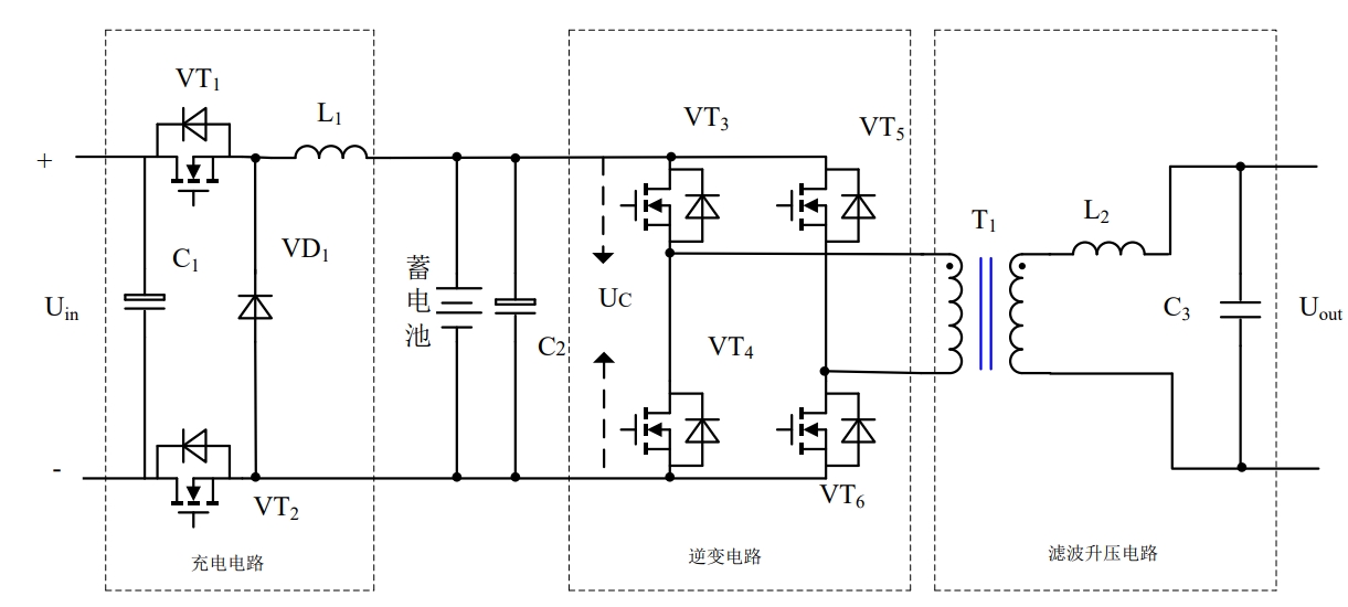
(1) Charging circuit
The charging circuit is a DC conversion circuit. Currently, the basic DC conversion circuits include buck chopper circuit (Buck circuit), boost chopper circuit (Boost circuit), boost-buck chopper circuit (Boost-Buck circuit), and Cuk circuit.The voltage output by the solar panel is 36V-48V, which is higher than the battery voltage of 24V, so the battery charging circuit uses a Buck circuit.
According to the working principle of the Buck circuit, the relationship between the input voltage UO and the output voltage Ui of the charging circuit in Figure 9 is:
Assuming that the value of L1 is sufficiently large, then:
From the combination of 17 and 18, we can obtain:
That is:
where ton is the VT1 on-time, toff is the VT1 off-time, T is one switching period, and α is the on-duty ratio.
According to equation 2-20 and the output characteristics of solar cells, when changing the on-duty ratio of VT1
α can change the size of the output load impedance. According to the output characteristics of solar cell modules, by continuously changing α, the output power of solar cells can be continuously adjusted to achieve the purpose of maximum power tracking of solar cell modules.
The MOS tube VT2 in the battery charging circuit is used to prevent current backflow when the battery voltage is higher than the solar cell voltage. When the system is operating normally, the solar cell output current is large. If a diode is used instead of VT2, the power loss will be large and the heat dissipation requirements will be high.Therefore, a MOS tube is used to complete the task.When the battery voltage is detected to be higher than the solar cell component voltage, VT2 is turned off to prevent backcharging.
(2) Inverter circuit
The inverter circuit converts DC input voltage into AC voltage output. Common inverter circuits include full-bridge inverter and half-bridge inverter. Compared to the half-bridge inverter circuit, the full-bridge inverter circuit has a reduced switching current by half, making it more suitable for high-power applications.In addition, the full-bridge inverter circuit can better utilize DC voltage.Therefore, the full-bridge inverter circuit used in this article.
The inverter circuit in Figure 9 is a schematic diagram of a full-bridge inverter circuit. When the switch tubes VT3 and VT6 are simultaneously turned on, the output voltage Uout is positive. When VT4 and VT5 are simultaneously turned on, the output voltage Uout is negative.However, the two switch tubes in the same half bridge cannot be simultaneously turned on to avoid short circuiting the circuit.
(3) Filtering and boosting circuit
The LC low-pass filter circuit used in this article eliminates the high-order harmonics in the output voltage of the inverter circuit, resulting in a low-voltage sinusoidal current of 50Hz. The input and output are electrically isolated through a power frequency transformer, and the voltage is raised to a sinusoidal current with an effective value of 220V.
5. Hardware circuit parameter design
5.1 Filter circuit design
(1) Input filter capacitor
In order to reduce the ripple of the input voltage caused by load changes, we incorporate an input filter capacitor on the input side of the circuit, using its energy storage principle to stabilize the input voltage. The energy it needs to provide per cycle is:
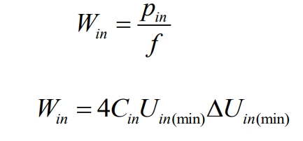
Wherein: Pin is the input power
f is the operating frequency of the capacitor
Uin(min) is the minimum input DC voltage
ΔUin(min) = 1%Uin(min)
From Equations 21 and 22 above, the input filter capacitance value is 4400 μF.
(2) Output filter circuit
The solar inverter outputs AC voltage from the input DC voltage through SPWM control. After being boosted by the transformer, it contains a large amount of high-order harmonics. In order to improve the waveform quality and obtain high-quality sine waves that meet our needs, an LC low-pass filter circuit needs to be added at the output end.
Equation 23 is the transfer function of the LC filter circuit:
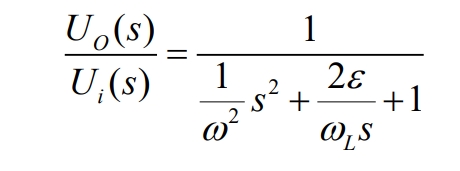
Where: ωL = 1/√ ̄LC (LC resonant angular frequency)
ε is the damping coefficient
S is Laplace factor
Cut-off frequency of the filter:
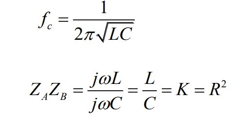
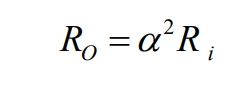
Wherein, K is a constant coefficient
ZA is the series impedance
ZB is the parallel impedance
R is the characteristic impedance, which is taken as (0.5-0.8 times the load impedance)
The system input is a DC 24V voltage, and the output is a 220V/50Hz sinusoidal voltage. The inductance and capacitance values can be calculated using equations 23, 24, and 25.The inductance selected in this design is 39μH
The capacitance value is 0.68μF.
5.2 Design of ring power frequency transformer
The design of the ring power frequency transformer includes: selecting the core material, determining the core specifications, designing the winding turns of the primary and secondary sides, and selecting the winding diameter.
(1) Specification of iron core
According to the formula for transformer capacity and core cross-sectional area:
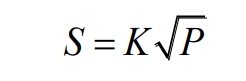
Where, K is the coefficient, taking the value of 0.8;S is the cross-sectional area of the iron core;P is the transformer capacity.
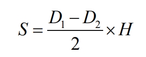
Wherein, D1 is the outer diameter of the transformer (cm);D2 is the inner diameter of the transformer (cm);H is the height of the circular ring.
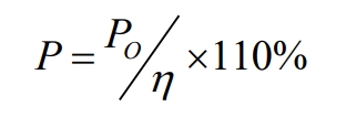
Wherein, η is the transformer efficiency, taken as 0.95, and Po is the system design rated output power of 500W, with a maximum allowable output power of 110% of the design power.
From equations 26, 27, 28 and the corresponding data, we can obtain:
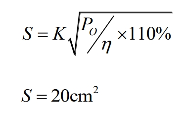
The core size height is H=4cm, the outer diameter D1=20cm, and the inner diameter D2=15cm.
(2) The original number of secondary winding turns
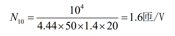
The number of turns per volt of the primary winding:
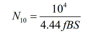
Where, f is the voltage frequency (50Hz), B is the magnetic flux density (choosing B as 1.4T silicon steel sheet), and the belt type 31 is:
Effective value of primary voltage:
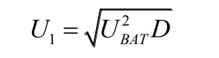
Wherein: the output voltage of lead-acid battery UBAT=24V, and the duty cycle of full-bridge inverter D=0.45, :
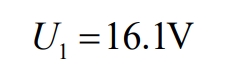
Then N1=N10U1=1.6X16.1=26 turns.
(3) Number of turns per volt of the secondary winding:
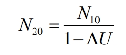
Where ΔU≤ 7% is the voltage regulation rate, which is brought into equation 33:
Then N2 = N20U2=1.72 X 220 = 378.5 turns, taking N2 = 379 turns.
(4) Selecting the diameter of winding wire
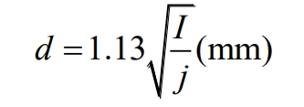
Diameter of winding wire:
Wherein, I is the current passing through the wire (A);
j is the current density, j = 2.5 ~ 3A/mm^2
When j = 2.5A/mm^2, it can be seen from equation 34 that:
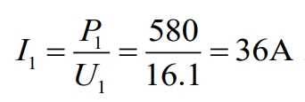
The maximum input power of the primary side is P1=580W, and the maximum output power of the secondary side is P2=550W, then the input current is:
Output current:
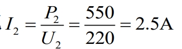
The 35 rules are:
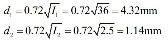
As the maximum diameter of the enameled wire is 2.44, which does not meet the requirements, the original winding is selected to use 4 enameled wires with d=2.26mm and an outer diameter of 2.36mm, and the cross-sectional area of the 4 enameled wires of this size is:
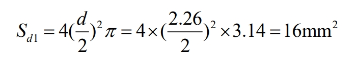
The cross-sectional area of the enameled wire with a diameter of 4.33mm is:
Therefore, it meets the requirements and has sufficient margin;the secondary side uses enameled wire with a diameter of 1.16mm and an outer diameter of 1.24mm.
5.3 Calculation of Buck inductance
The Buck circuit has two operating modes: continuous inductor current mode (CCM) and discontinuous inductor current mode (DCM).The charging circuit designed in this article uses a Buck circuit with continuous inductor current mode.The appropriate selection of inductor value in the circuit directly affects the quality of the output current. In order to control the ripple of the current within our acceptable range, and without using too large inductor, we need to calculate the inductor value and select the appropriate inductor.
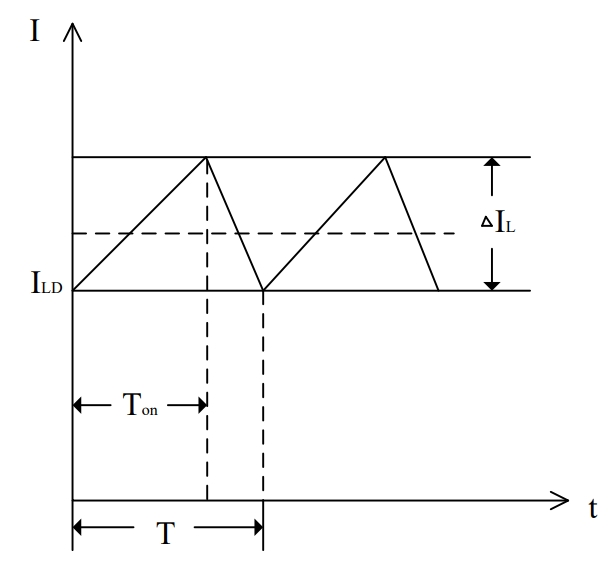
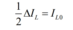
According to Figure 10, the current in the inductor can be divided into two components: a steady DC current IL0 and a ripple current ΔIL.When the Buck circuit operates in a critical state of intermittent and continuous operation, the relationship is given by Equation 36:
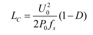
The corresponding inductance value at this time is:
Among them:
LC is the critical inductance value;
fs is the switching frequency;
P0 is the output power of the circuit;
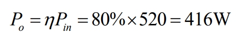
The maximum output power of the solar cell is 520W, and the power conversion efficiency of the Buck circuit is η is generally 80%, and after transformation, the circuit output power is:
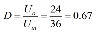
The maximum power point output voltage Uin of the solar cell is approximately 36V, and the battery terminal voltage Uo is approximately 24V. Therefore, the on-state duty cycle of the switch tube is:
Then the critical inductance value can be obtained as: LS = 23.1μH
We choose an inductance value of L = 60μH, leaving enough margin for the system.
5.4 Switch tube selection
The commonly used fully-controlled power switch tubes mainly include IGBT and MOSFET. The structural differences between the two lead to their respective advantages and disadvantages.IGBT is easier to drive, has a smaller voltage drop during conduction, and can withstand high voltages, but its high-frequency characteristics are poor and the switching loss is relatively large, which is generally applied in high-power applications.MOSFET has good high-frequency characteristics, and the solar inverter power designed in this article is relatively small, which is a voltage-driven device with good breakdown resistance, suitable for applications in low-power situations.
The designed solar inverter has a rated output power of 500W, and MOSFET is suitable for this design. Through the calculation of inverter related parameters, we selected the IRF3205PbF MOSFET from IR company, which is a standard N-channel field effect transistor. Its corresponding parameters are as follows:
The drain-to-source voltage is Vdss=55V;
The drain-to-source resistance is RDS(on)=8mΩ;
Current – continuous drain ID=110A;
Maximum power PMAX=200W.
When the output is at rated load, each bridge arm of the inverter circuit requires 275W of power from a MOS tube, while the maximum power that the switch tube can withstand is 200W. Therefore, in practical applications of this circuit, two switch tubes are used in parallel to perform shunt action and reduce their power tolerance.
6. Control circuit design
6.1 Control chip
This design uses the TMS320F28023DSP, which is designed by TI. This control chip has strong computing power, multiple peripheral resources, small size, low price, convenient portability, good maintainability, and easy expansion, which can effectively control the system.The control chip performs digital conversion on the analog signals fed back by the peripheral circuit, performs calculations, and obtains the required control signals. After amplification by the relevant circuits, it achieves effective control of the switch tube.
The TMS320F28023 DSP uses high-performance static CMOS technology, with the following specifications: instruction cycle of 20ns;32K×16-bit on-chip flash memory;6K×16-bit on-chip SARAM;12K×16-bit RAM. The main resource configurations are:
(1) Equipped with a 32-bit C281X CPU core, it has 32-bit fixed-point digital processing capabilities;16×16-bit and 32×32-bit multiplication and accumulation operations;a main frequency of 50MHz, Harvard bus architecture;unified addressing mode, 4MB data/program addressing space;fast code conversion function, programming can be done using C/C++, assembly language, compatible with TMS320F24x/F240x series digital signal processor code.
(2) Introduction to C281x peripherals: There are two event managers, EVA and EVB, each of which includes: comparators, timers, PWM logic circuits, capture units, interrupt circuits, orthogonal encoded pulse circuits, etc. A 13-channel 12-bit ADC module converts external analog signals into digital values with a conversion rate of 3MSPS and a conversion time of 260ns. It supports dual sample and hold, temperature sensors, and a serial peripheral interface (SPI) and a serial communication interface.An internal integrated circuit (I2C) is also included.The bus interface is an enhanced CAN interface that fully supports the CAN2.0B bus specification.Watchdog/interrupt modules;28 shared I/O pins, including 22 GPIOs and 6 AIOs;external interrupt and expansion modules, supporting all peripheral interrupts;built-in undervoltage and power-on reset circuits;8 enhanced pulse width modulator EPWM modules, each with independent analog comparators and 16-bit timers;providing OTP-type read-only memory, root read-only memory, Flash memory, and single-port random access memory.
As the core device of system control, it mainly implements the following control functions in system operation:
(1) Based on the battery voltage and charging current feedback from the sampling circuit, the charging and discharging of the battery is controlled to prevent overcharging and overdischarging.
(2) Achieve maximum power tracking of solar cells.
(3) According to the comparison between the output power of solar cells and the required power of the load, the system can operate under different working modes. When the output power of solar cells cannot meet the load demand, the battery and solar cells simultaneously supply power to the load.When the output power of solar cells is greater than the required power of the load, the charging method of the battery is selected according to the state of the battery’s stored electricity.
(4) Based on the feedback signals of the inverter output voltage and current, achieve stable control of the output voltage and prevent system overload.
6.2 Modulation of SPWM
The generation of PWM waveforms can be controlled by modulation and calculation methods. If obtaining the required PWM through calculation is very complex, it will not be explained in detail in this article.The principle of obtaining SPWM waveforms through modulation is to compare the sawtooth wave (carrier wave) with the sine wave (modulation wave) through a comparator.In the control chip, the simulated sawtooth wave can be achieved by continuous increasing and decreasing count of the counting register, and then comparing it with the sine wave in the register to obtain the corresponding SPWM wave. By continuously changing the amplitude of the sine wave through feedback signals, the width control of the SPWM wave can be achieved, so as to control the on-duty ratio of the switch tube and continuously adjust the amplitude of the output voltage.The frequency of the sine wave in this article is achieved by using a simple and highly reliable look-up table method.
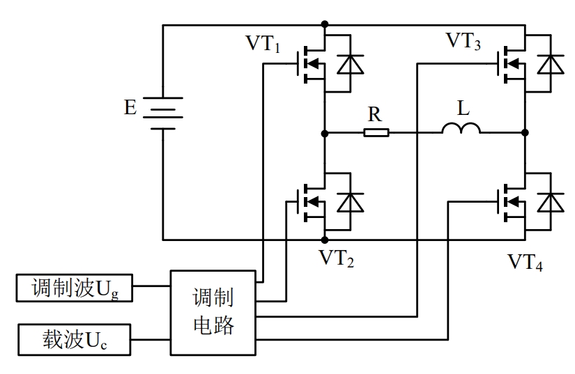
Figure 11 shows a single-phase full-bridge PWM inverter circuit.VT1 and VT4 form switch tube group 1, and VT2 and VT3 form switch tube group 2. When both switch tubes in switch tube group 1 are in the on state, the output voltage is positive. When switch tube group 1 is in the off state, and both switch tubes in switch tube group 2 are in the on state, the output voltage is negative.The two switch tube groups are constantly alternating conduction to achieve voltage inversion.In the conduction process, the VT1, VT2, VT3, VT4 switch tubes in the same half bridge cannot be in the on state at the same time to avoid the phenomenon of direct conduction and damage to the switch tubes. In the circuit, the on and off states of the two switch tubes in each half bridge are complementary, but a certain dead time is reserved when exchanging the on and off states to avoid direct conduction of the two switch tubes in the same half bridge.
The modulation method of SPWM is divided into two categories: unipolar modulation and bipolar modulation.
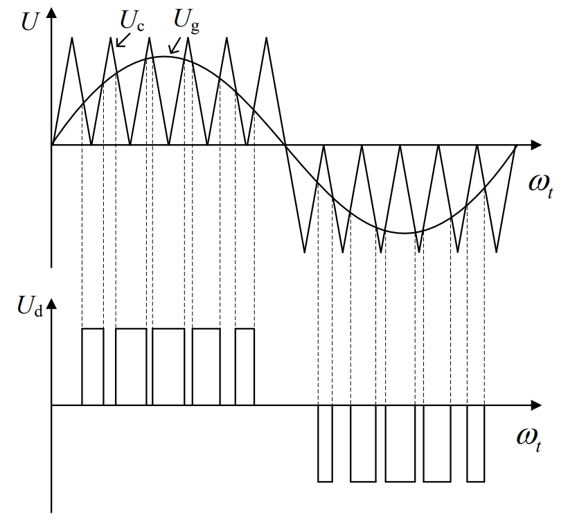
(1) Monopolar modulation
Figure 12 shows the unipolar control mode. When the solar inverter output voltage is in the positive half cycle, VT1 is always in the on state, VT2 is in the off state, and the SPWM wave Ud modulated by Ug (sinusoidal modulation wave) and Uc (triangle carrier wave) controls the on and off states of VT3 and VT4. When Ud is positive, VT3 is controlled to be on, and when Ud is negative, VT4 is controlled to be on.
(2) Bipolar modulation
Figure 13 shows the bipolar modulation method, where the modulated SPWM wave is positive when VT1 and VT4 are conducting and negative when VT2 and VT3 are conducting. We can see that during the positive half-cycle of the sine wave, there is also a negative pulse, which causes the output voltage to have a negative output voltage. Similarly, during the negative half-cycle of the sine wave, there is also a positive pulse, which causes the output voltage to have a positive output voltage.However, during the positive half-cycle, the effective value of the average voltage is positive, while during the negative half-cycle, the effective value of the voltage is negative.The required sine wave is output through a filtering circuit.
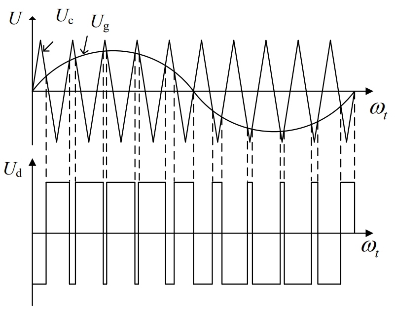
From the above two methods, it can be seen that there is a negative (positive) voltage output in the positive (negative) half-cycle of bipolar modulation, while the output voltage of unipolar modulation has lower mid- and high-order harmonic components than bipolar modulation. Therefore, this article adopts unipolar modulation. In order to improve the frequency of the output waveform and better filter out harmonics, unipolar frequency doubling modulation is selected to double the frequency of the output waveform without increasing the switching frequency.
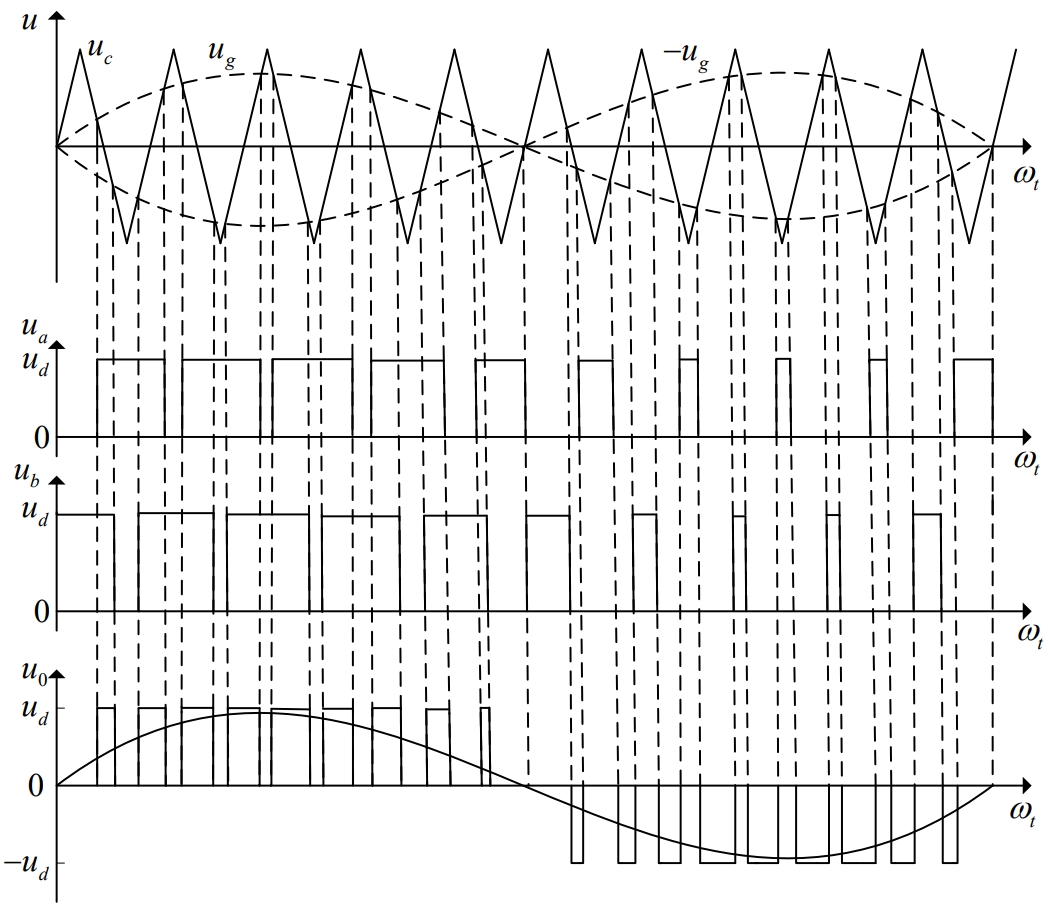
(3) Single-pole frequency multiplication modulation
Figure 14 shows the principle of SPWM modulation with unipolar frequency doubling. During the unipolar frequency doubling modulation process, the triangular carrier wave Uc is compared with two sinusoidal modulation waves, which have equal frequencies but a phase difference of 180o, i.e., the magnitudes are opposite.The comparison of the sinusoidal wave Ug with the triangular wave Uc produces one SPWM signal Ua, and the comparison of the sinusoidal wave-Ug with the triangular wave Uc produces another SPWM signal Ub. Using Ua to drive the switch tube VT1 and Ub to drive the switch tube VT2, the on-off complementarity of VT1 and VT2 is achieved.Using Ub to drive the switch tube VT4 and Ug to drive the switch tube VT3, the on-off complementarity of VT3 and VT4 is also achieved.From the above description, it can be seen that only when Ua and Ub are both high, VT1 and VT4 will be simultaneously turned on, and the solar inverter will output a positive voltage Ud.Similarly, only when Ua and Ub are both low, VT2 and VT3 will be simultaneously turned on, and the solar inverter will output a negative voltage -Ud.However, within one high-level pulse of Ua, the output voltage will have two high-low transitions, which doubles the output voltage frequency relative to the switching frequency.
7. DSP peripheral circuit design
7.1 Full bridge inverter circuit drive circuit
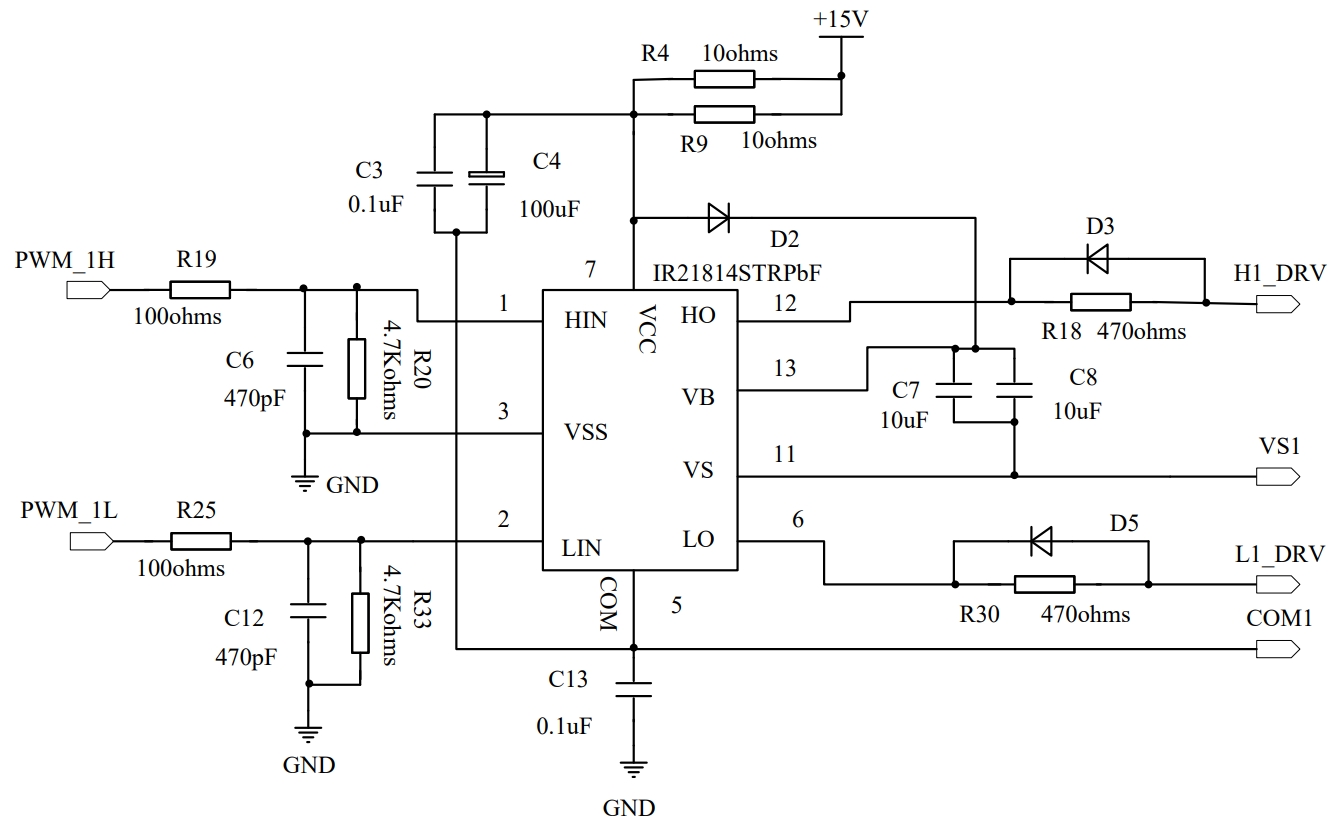
Figure 15 shows the drive circuit for the switch tubes of the full-bridge inverter circuit.The drive chip uses IR21814STRPBF, which provides a drive circuit for the reference-to-ground power transistor. It is controlled by the voltage difference between pin 5 and pin 6. The drive circuit for the high-side transistor is controlled by the voltage difference between pin 11 and pin 12.Pin 1 and pin 2 input two complementary SPWM control signals.Inside the chip, the input control signal on pin 2 determines the output on pin 6. When pin 2 is input high, pin 6 and pin 7 are connected, while pin 5 is always connected to ground. Then, a high level of 15V is output between pin 5 and pin 6.When pin 2 is input low, pin 6 and pin 5 are connected, and a low level is output between the two pins.The internal principle of the other drive signal output is the same. When pin 1 is input high, pins 12 and 13 are connected, and the output is the potential difference between parallel capacitors C7 and C8. When pin 1 is input low, pins 11 and 12 are connected and output a low level.The parallel capacitors C7 and C8 together form a bootstrap capacitor. When the reference-to-ground switch tube is on and the voltage between pin 5 and pin 6 is high, pins 11 and 12 are connected and also connected to ground. During this process, the 15V power supply will charge the bootstrap capacitor set, forming a 15V potential difference between its two ends.When pins 12 and 13 are connected, a high level of 15V will be output at both ends.
7.2 Charging circuit drive circuit
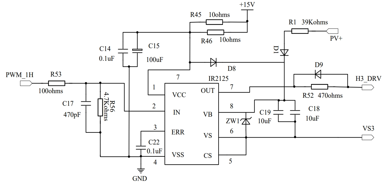
Figure 16 shows the driving circuit of the Buck circuit. When the switch tube is driven by the high-end voltage, the freewheeling diode is turned on during the operation of the Buck circuit, which lowers the voltage level of pin 6 and charges the bootstrap capacitor C18 and C19, forming a 15V potential difference between pins 6 and 8. When the SPWM control signal input pin 2 is high, pin 7 and pin 8 are turned on, and the control pulse output between pins 6 and 7 is high.However, because the rear stage of the Buck circuit is a battery, the voltage at pin 6 is the battery voltage, which is higher than 15V before the circuit starts working.The bootstrap capacitor is not charged. When the SPWM input is high, there is no high-level output between pins 6 and 7. Therefore, the driving circuit is shown in Figure 16, using the driving chip IR2125.R1 is added to the circuit to provide another charging method for the bootstrap capacitor.Since the open-circuit voltage of the PV+ voltage before operation is basically above 40V, which is higher than the battery voltage, the current will pass through R1 to charge the bootstrap capacitor. To prevent the voltage of the bootstrap capacitor from being too high, a 15V zener diode ZW1 is connected in parallel with the bootstrap capacitor. Therefore, before the circuit starts working, there will be a 15V potential difference between the two ends of the bootstrap capacitor, providing a starting pulse for the circuit.
7.3 Auxiliary power supply circuit
The power circuit is the driving force for system operation, and the quality of the auxiliary power output voltage directly affects the system control effect. It mainly provides a stable 3.3V operating voltage for the control chip and a 15V operating voltage for the drive circuit. The charging circuit in this system consists of three parts:
(1) The output voltage of the battery will fluctuate with the change of stored electricity. After the output of a stable output voltage through a triode voltage regulator circuit, as shown in Figure 17, the stable voltages of the voltage regulator diodes VD1 and VD2 are 5.1V and 18V respectively. The base voltage of the triode is stabilized at 23.1V. There is a diode between the emitter and base of the triode, which has a voltage drop of 0.7V when conducting.Therefore, the output voltage is stabilized at 22V.
Figure 18 shows a power supply circuit designed using the asynchronous DC/DC buck chip TPS54331, which provides a working voltage of 3.3V DC for the control chip. The chip’s input voltage is 3.5V to 28V, and the adjustable output voltage is 0.8V-25V. It can continuously output a maximum DC current of 3A. Its output voltage can be expressed using Equation 38:
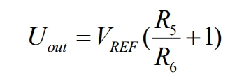
Where VREF is the internal reference voltage of the chip, with a value of 0.8V. The output voltage is determined by changing the resistance values of resistors R5 and R6. When we take R5 to be 4.7KΩ and R6 to be 1.5KΩ, the output voltage is 3.3V.
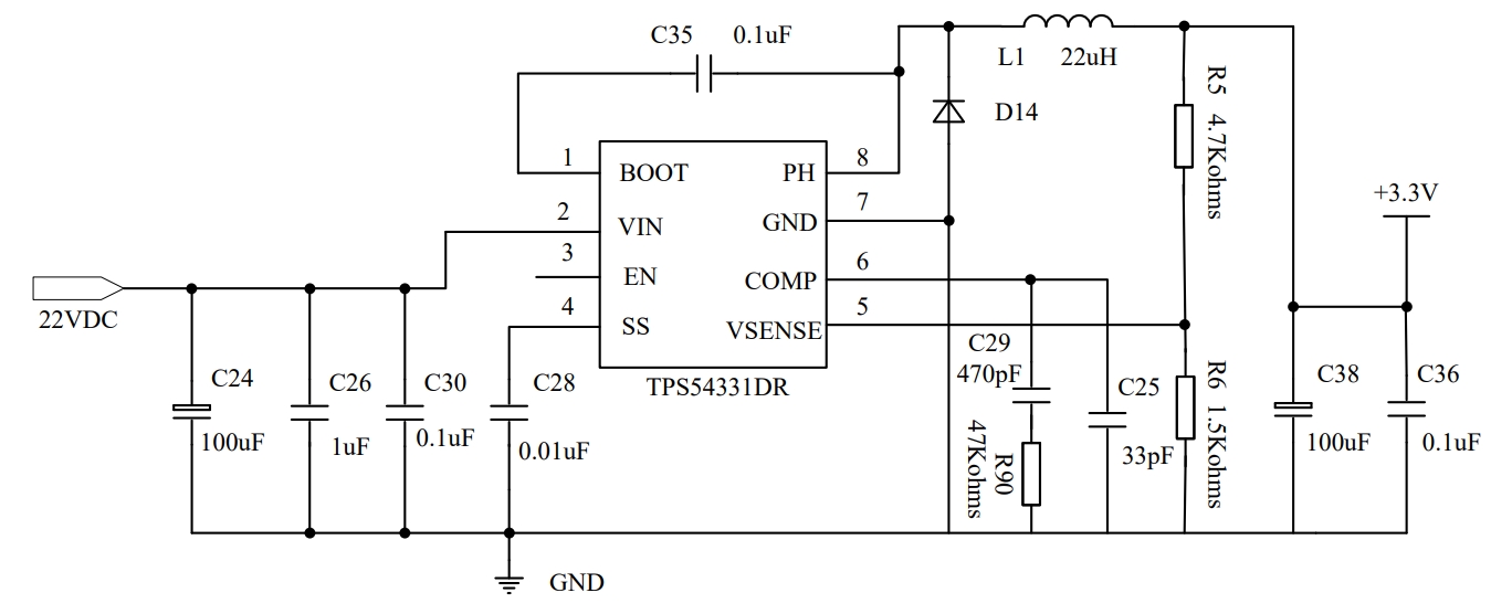
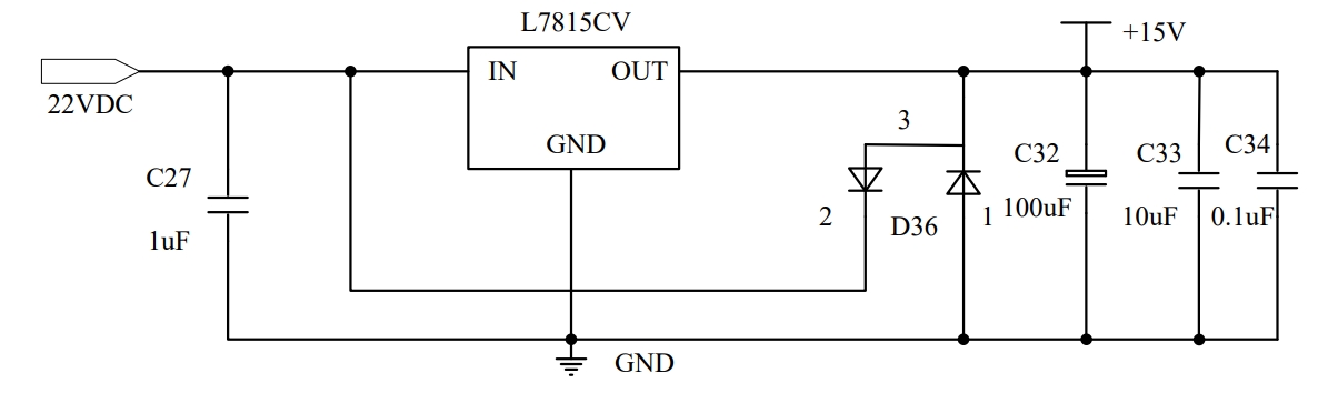
Figure 19 shows a 15V power supply circuit implemented using the L7815CV chip. The chip has an input voltage range of 17V-35V, an output voltage of 15V, and a maximum output current of 1.5A.
7.4 Sampling circuit
In order to ensure the safe and stable operation of the system and enable the system to output the results we need, the required system parameters are collected through sampling circuits, and the signals are processed through filtering and op-amp circuits to obtain the control signals required by the control chip.The required sampling signals mainly include: AC output voltage and current;solar cell output voltage and current;battery charging voltage and current;system and battery temperature.
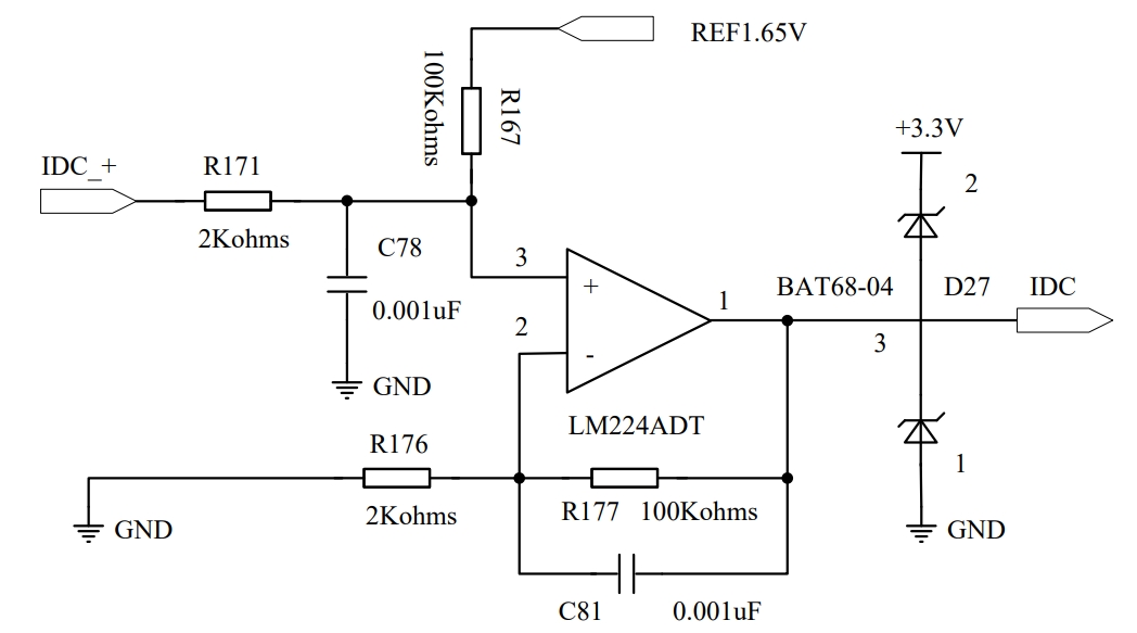
Figure 20 shows the DC current sampling circuit. The sampling resistor connected in series in the circuit converts the current at the sampling point into a voltage signal and transmits it to the IDC_+ terminal.An op-amp module of LM224ADT amplifies the signal by 50 times, and resistors R171 and R167 raise the voltage by 1.65V. Then, the signal is clamped and limited below 3.3V by BAT68-04, and the sampling signal is transmitted to the control chip.
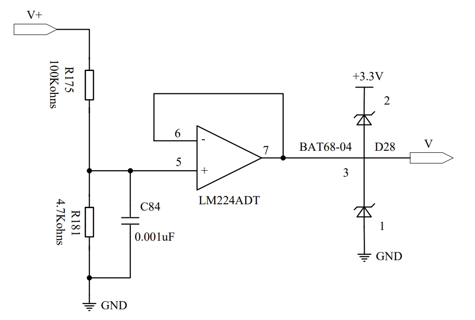
Figure 21 shows the DC sampling circuit, which connects the sampling point to the input terminal V+. After voltage division by resistors R175 and R181, the voltage is followed by an op-amp module provided by LM224ADT. The output signal is clamped and limited to below 3.3V by BATT68-04 and input to the control chip.
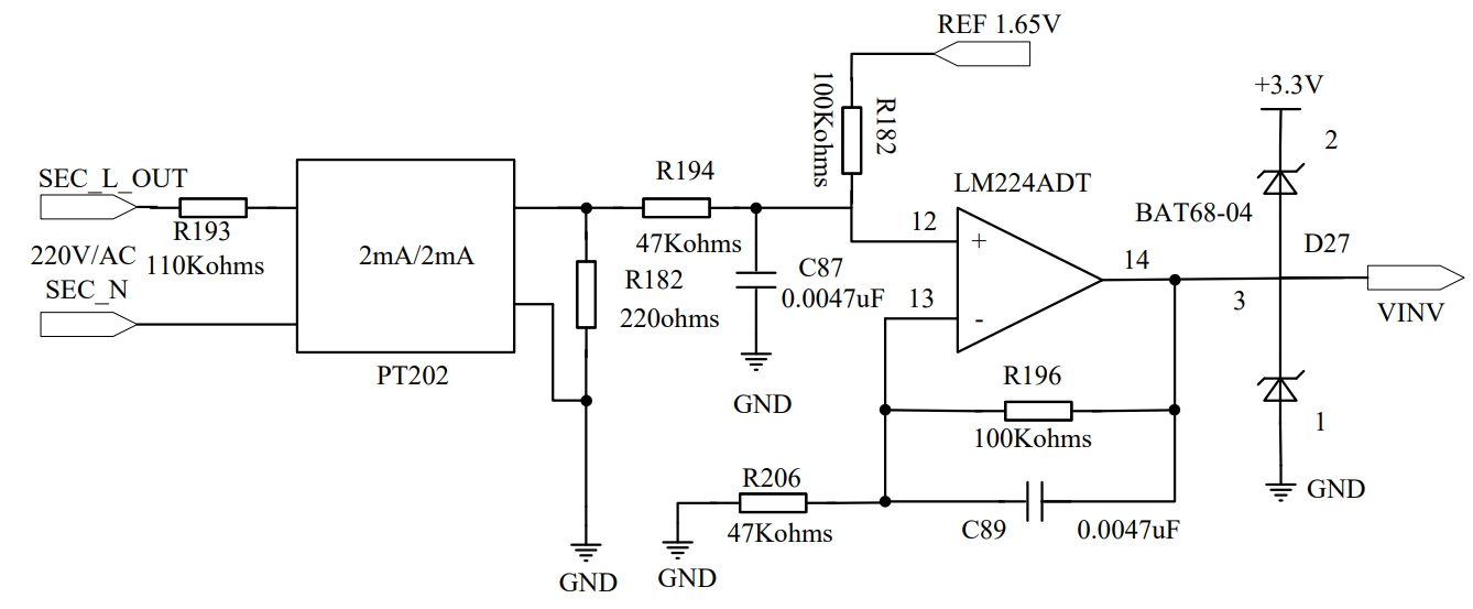
Figure 22 shows the AC voltage sampling circuit.The AC voltage output by the system is connected to the input terminals SEC_L_OUT and SEC_N of the sampling circuit.After being isolated by the current-type voltage transformer PT202, the sampling voltage is obtained across the resistor R182, and is output to the No. 14 pin by a power amplifier module of LM224ADT. During this process, the voltage sampling signal is amplified by R183/R194 times, limiting the voltage between -1.65V and +1.65V. Then, the voltage is raised by 1.65V, so that the sampling voltage signal output by the No. 14 pin is between 0-3.3V. After being clamped and limited by BAT68-04, it is sent to the control chip.
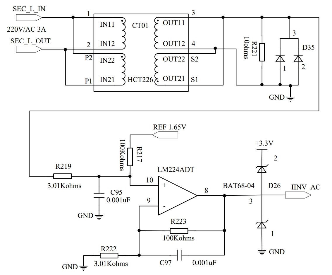
Figure 23 shows the AC current sampling circuit.The current transformer HCT226HJZ-2 is selected, with a transformation ratio of 5A:2.5mA, an accuracy of 0.05%, and an isolation voltage of 4000Vac. The output terminal is connected in parallel with a resistor R221, which converts the AC signal into a voltage signal. The voltage signal is then amplified by a power amplifier circuit by a factor of R223/R222, and raised by 1.65V, so that the signal varies within the amplitude range of 0-3.3V. After passing through the clamping and limiting circuit, it is output to the control chip.
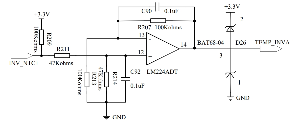
Figure 24 shows the system temperature sampling circuit. Due to the temperature-dependent resistance characteristics of the temperature sensor, the voltage across R214 varies with temperature. Due to the voltage division of R211, the voltage drop across R214 is less than 1.65V, which means that the voltage at pin 12 of LM224ADT is less than 1.65V. After passing through the power amplifier circuit, the output voltage at pin 14 is twice the voltage at pin 12 and is less than 3.3V. After passing through the D26 clamp and limiting circuit, it is sent to the control chip.
7.5 Protection circuit
To ensure the safe and stable operation of the system, it is necessary to limit the maximum and minimum values of relevant parameters in the control chip, such as determining excessive current, low battery voltage, high system temperature, system short circuit, etc. If the corresponding feedback signal exceeds the system setpoint, appropriate measures will be taken, such as blocking the corresponding SWPM signal output, performing corresponding internal interruptions, terminating the corresponding program running, etc., to avoid system damage and issue an alarm signal.
8. Summary
Through the investigation of household electricity consumption in areas without electricity, the models of solar cells and batteries were determined, and the overall structure of the system was determined according to design requirements. The hardware main circuit of the solar inverter was designed, and the relevant parameters were calculated. The power switch tube and control chip suitable for this article were selected, and the peripheral auxiliary circuits of the control chip were designed and analyzed: auxiliary power supply circuit, sampling point circuit, drive circuit, and protection circuit.Through the research and comparison of SPWM modulation methods, the full-bridge inverter control method was determined.