
In my extensive experience designing and implementing power electronics systems, I have consistently observed that solar inverters are pivotal components in renewable energy infrastructure. These devices convert the direct current (DC) generated by photovoltaic panels into alternating current (AC) suitable for grid integration or local consumption. The efficiency and reliability of solar inverters hinge on robust isolation and noise immunity, areas where photocouplers play an indispensable role. This article delves into design strategies that leverage photocouplers to achieve superior power buffering and resilience against electrical noise, ensuring optimal performance in diverse solar inverter applications. Throughout this discussion, I will emphasize the critical importance of solar inverters in modern energy systems, and I will incorporate mathematical models and comparative tables to elucidate key concepts.
Solar inverters operate in demanding environments characterized by high voltages and transient spikes. The conversion process typically involves DC-DC and DC-AC stages, where photocouplers provide galvanic isolation between low-voltage control circuits and high-power switching components. This isolation prevents damage from voltage surges and minimizes signal distortion, which is crucial for maintaining the integrity of power conversion. In solar inverters, whether configured as micro-inverters for individual panels or central inverters for panel arrays, photocouplers serve as gate drivers for power transistors like IGBTs and MOSFETs. Their ability to buffer power signals while offering high common-mode rejection makes them ideal for these applications.
To understand the role of photocouplers, consider the basic architecture of a solar inverter. A micro-inverter, integrated into a single photovoltaic panel, handles power levels generally below 1 kW, while central inverters manage arrays at power levels exceeding 10 kW. Both types rely on photocouplers to drive the gates of power semiconductors in half-bridge or full-bridge configurations. The photocoupler acts as a buffer, translating control signals from a microcontroller into gate-drive currents that switch high-voltage transistors on and off. This process must be efficient and noise-resistant to maximize the overall efficiency of the solar inverter system.
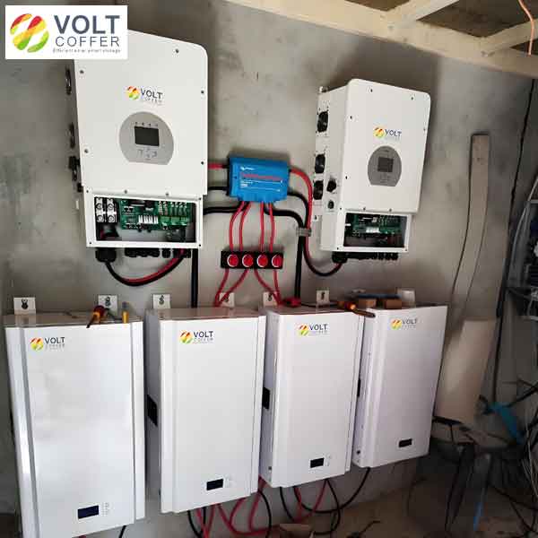
The image above illustrates a hybrid solar inverter configuration, showcasing the compact design typical of modern systems. Such inverters often incorporate photocouplers for isolation in gate-drive circuits, highlighting their integration in real-world applications. In my designs, I prioritize photocouplers with high isolation ratings and fast switching capabilities to handle the rigorous demands of solar inverters.
One of the primary challenges in solar inverter design is managing startup sequences. When power is initially applied, multiple supply rails—such as logic supply, photocoupler supply, and high-voltage supply for power transistors—must stabilize in a specific order to avoid spurious gate-drive outputs. I recommend the following sequence: first, activate the logic supply; second, enable the photocoupler supply; and third, power the high-voltage DC bus. This sequence mitigates delays caused by photocoupler bias stabilization and aligns with control logic initialization. Mathematically, the stabilization time can be modeled using a first-order RC circuit approximation:
$$V_{bias}(t) = V_{final} \left(1 – e^{-\frac{t}{\tau}}\right)$$
where $\tau = R_{bias} C_{bias}$ represents the time constant of the bias network. By ensuring that the photocoupler supply ramps up before high-voltage switching, we minimize the risk of false triggering, which is critical for the reliable operation of solar inverters.
Common-mode rejection (CMR) is another vital parameter for photocouplers in solar inverters. High CMR ensures immunity to fast transient noise generated during switching events, which can couple through parasitic capacitances. The CMR rating, typically expressed in kV/µs, indicates the maximum rate of voltage change that the photocoupler can withstand without erroneous output switching. For instance, a photocoupler with a CMR of 50 kV/µs can reject transients with slew rates up to that value. The coupling capacitance $C_{coupling}$ between input and output plays a key role, as the noise current $I_{noise}$ induced by a common-mode transient $V_{cm}$ is given by:
$$I_{noise} = C_{coupling} \frac{dV_{cm}}{dt}$$
To enhance noise immunity, I employ photocouplers with low coupling capacitance (often below 1 pF) and incorporate shielding techniques. Additionally, using current-mode driving for the photocoupler input can further reduce susceptibility. The following table summarizes key characteristics of two exemplary photocouplers suitable for solar inverters, emphasizing parameters that impact power buffering and noise performance:
| Parameter | Photocoupler A | Photocoupler B |
|---|---|---|
| Supply Voltage Range | 15 V to 30 V | 15 V to 30 V |
| Output Current Capability | 2.5 A peak | 2.5 A peak |
| Isolation Voltage | 3750 VRMS | 3750 VRMS |
| Common-Mode Rejection (CMR) | 50 kV/µs minimum | 50 kV/µs minimum |
| Propagation Delay | 100 ns typical | 150 ns typical |
| Coupling Capacitance | 0.8 pF | 0.6 pF |
| Maximum Switching Frequency | 500 kHz | 400 kHz |
These characteristics directly influence the efficiency and reliability of solar inverters. For example, a high CMR ensures stable operation in noisy environments, while low propagation delay minimizes power losses during switching. In my designs, I select photocouplers based on such tables to match the specific requirements of the solar inverter, whether it is a low-power micro-inverter or a high-power central inverter.
Parallel driver configurations offer another technique to boost noise immunity in half-bridge setups common in solar inverters. By connecting an additional driver in parallel with the main photocoupler, we create a current shunt that reduces the effective impedance seen by common-mode noise currents. This approach is particularly useful in solar inverters where switching transients can exceed 100 V/ns. The equivalent circuit can be analyzed using Kirchhoff’s current law:
$$I_{total} = I_{photocoupler} + I_{parallel}$$
where $I_{parallel}$ is sourced from the parallel driver. However, this method introduces additional power dissipation, which must be accounted for in thermal calculations. The power loss $P_{loss}$ in the parallel driver can be estimated as:
$$P_{loss} = I_{parallel}^2 \cdot R_{on} + V_{drop} \cdot I_{parallel}$$
where $R_{on}$ is the on-resistance and $V_{drop}$ is the voltage drop across the driver. Balancing noise immunity with efficiency is a key consideration in solar inverter design, and I often simulate these trade-offs using circuit modeling tools.
Maximum switching frequency is a critical limit for photocouplers in solar inverters, as it dictates the inverter’s power density and control bandwidth. The frequency is constrained by the photocoupler’s propagation delays and power dissipation. To calculate the maximum frequency $f_{max}$, I use the following formula derived from thermal constraints:
$$f_{max} = \frac{P_{diss,max} – P_{DC}}{C_{gate} \cdot V_{gate}^2 \cdot (t_{rise} + t_{fall})}$$
where $P_{diss,max}$ is the maximum allowable power dissipation at the junction temperature (e.g., 150°C), $P_{DC}$ is the steady-state power loss, $C_{gate}$ is the gate capacitance of the power transistor, $V_{gate}$ is the gate-drive voltage, and $t_{rise}$ and $t_{fall}$ are the rise and fall times of the photocoupler output. For solar inverters operating at high power levels, optimizing $f_{max}$ enables higher switching frequencies, which reduce filter sizes and improve response times. I typically aim for frequencies in the range of 20 kHz to 100 kHz, depending on the solar inverter topology.
Noise mitigation extends beyond CMR to include layout practices. In solar inverters, minimizing loop areas and using dedicated ground planes for control and power sections reduces inductive coupling. I also recommend placing decoupling capacitors close to photocoupler supply pins to suppress high-frequency noise. The effectiveness of decoupling can be quantified by the impedance $Z_{decouple}$ at the target frequency:
$$Z_{decouple} = \sqrt{R_{ESR}^2 + \left(2\pi f L_{parasitic} – \frac{1}{2\pi f C_{decouple}}\right)^2}$$
where $R_{ESR}$ is the equivalent series resistance, $L_{parasitic}$ is the parasitic inductance, and $C_{decouple}$ is the decoupling capacitance. By keeping $Z_{decouple}$ low, we ensure clean supply rails for photocouplers, enhancing overall stability in solar inverters.
Another aspect I consider is the start-up behavior of photocouplers in solar inverters. During initial power-up, the photocoupler’s internal amplifier may exhibit temporary output glitches if the bias supply is unstable. To prevent this, I implement soft-start circuits that gradually ramp the photocoupler supply voltage. The ramp time $t_{ramp}$ can be calculated based on the desired inrush current limit $I_{limit}$:
$$t_{ramp} = \frac{C_{supply} \cdot V_{final}}{I_{limit}}$$
where $C_{supply}$ is the total capacitance on the supply rail. This approach ensures smooth activation of gate drives, which is essential for preventing shoot-through currents in bridge configurations of solar inverters.
To further illustrate design trade-offs, I have compiled a table comparing different photocoupler integration strategies for solar inverters. This table helps in selecting the optimal approach based on power level, noise environment, and cost constraints:
| Strategy | Advantages | Disadvantages | Recommended Solar Inverter Type |
|---|---|---|---|
| Single Photocoupler per Gate | Simple design, low cost | Limited noise immunity | Micro-inverters (≤1 kW) |
| Parallel Driver Configuration | High CMR, robust in noisy settings | Increased power dissipation | Central inverters (≥10 kW) |
| Dual Photocouplers with Cross-Coupling | Redundancy, fault tolerance | Complex layout, higher component count | High-reliability solar inverters |
| Integrated Gate-Drive IC with Isolation | Compact, optimized timing | Less flexibility, vendor-dependent | Compact solar inverters |
In my practice, I often combine these strategies based on the specific needs of the solar inverter project. For instance, in a central solar inverter for industrial use, I might use parallel drivers for critical switches while opting for integrated solutions for auxiliary circuits.
Thermal management is also crucial for photocouplers in solar inverters, as excessive heat can degrade performance and longevity. The junction temperature $T_j$ can be estimated using the thermal resistance $\theta_{JA}$:
$$T_j = T_a + P_{diss} \cdot \theta_{JA}$$
where $T_a$ is the ambient temperature and $P_{diss}$ is the power dissipated in the photocoupler. For solar inverters operating in outdoor environments, I ensure adequate heatsinking or airflow to maintain $T_j$ below safe limits, typically 125°C for commercial-grade components.
Furthermore, safety certifications such as UL and IEC standards are mandatory for photocouplers in solar inverters, as they ensure compliance with isolation requirements. These standards specify creepage and clearance distances, which I verify during layout. For example, a photocoupler with 8 mm creepage distance is suitable for reinforced isolation in solar inverters up to 1000 VDC. The required distance $d_{creepage}$ can be derived from the working voltage $V_{work}$:
$$d_{creepage} \geq k \cdot V_{work}$$
where $k$ is a material-dependent constant (e.g., 0.025 mm/V for many insulating materials). Adhering to these standards is non-negotiable in solar inverter design to protect personnel and equipment.
In conclusion, photocouplers are indispensable for achieving reliable power buffering and noise immunity in solar inverters. Through careful attention to startup sequences, common-mode rejection, parallel driving, thermal design, and safety standards, we can optimize their performance. The mathematical models and tables presented here provide a framework for designers to make informed decisions. As solar inverters continue to evolve towards higher efficiency and power densities, advanced photocoupler technologies will remain at the heart of their success, enabling clean energy integration into grids worldwide. I encourage ongoing experimentation and simulation to refine these techniques, ensuring that solar inverters meet the growing demands of renewable energy systems.
To summarize key formulas discussed in this article, I list them below for quick reference:
1. Bias stabilization: $$V_{bias}(t) = V_{final} \left(1 – e^{-\frac{t}{\tau}}\right)$$
2. Noise current: $$I_{noise} = C_{coupling} \frac{dV_{cm}}{dt}$$
3. Parallel driver power loss: $$P_{loss} = I_{parallel}^2 \cdot R_{on} + V_{drop} \cdot I_{parallel}$$
4. Maximum switching frequency: $$f_{max} = \frac{P_{diss,max} – P_{DC}}{C_{gate} \cdot V_{gate}^2 \cdot (t_{rise} + t_{fall})}$$
5. Decoupling impedance: $$Z_{decouple} = \sqrt{R_{ESR}^2 + \left(2\pi f L_{parasitic} – \frac{1}{2\pi f C_{decouple}}\right)^2}$$
6. Soft-start ramp time: $$t_{ramp} = \frac{C_{supply} \cdot V_{final}}{I_{limit}}$$
7. Junction temperature: $$T_j = T_a + P_{diss} \cdot \theta_{JA}$$
8. Creepage distance: $$d_{creepage} \geq k \cdot V_{work}$$
These equations, coupled with the tabular data, form a comprehensive toolkit for enhancing photocoupler applications in solar inverters. By iteratively applying these principles, we can push the boundaries of what solar inverters can achieve, contributing to a more sustainable energy future.