
In recent years, the demand for flexible and efficient solar cells has grown significantly due to the rapid development of wearable electronic devices and building-integrated photovoltaic applications. Traditional rigid solar cells face limitations in these scenarios, prompting a shift toward flexible alternatives. Among these, perovskite solar cells have emerged as a promising candidate due to their high efficiency, tunable bandgaps, and low-cost fabrication processes. However, the integration of perovskite solar cells with silicon in a tandem configuration on flexible substrates presents unique challenges, including optimizing crystallization, enhancing light management, and ensuring mechanical and thermal stability. This study focuses on systematically addressing these issues by designing and optimizing a flexible perovskite-silicon tandem solar cell, with particular emphasis on improving photoelectric conversion efficiency and durability under bending and thermal stress.
The core of our approach involves using a polyimide substrate to construct a tandem structure comprising an upper perovskite layer and a lower silicon layer. We optimized the perovskite crystallization quality by introducing phenethylammonium iodide (PEA) as an additive, implemented a multilayer texture structure in the silicon bottom cell to enhance light trapping, and developed a MoO3/ITO composite tunneling junction to facilitate efficient electrical connection between the subcells. Through these strategies, we achieved a notable photoelectric conversion efficiency of 22.7%, along with excellent mechanical stability, with only an 8.2% performance degradation after 1,000 bending cycles, and stable output at operating temperatures up to 60°C. This work provides new insights into the development of high-performance flexible photovoltaic technologies for practical applications.
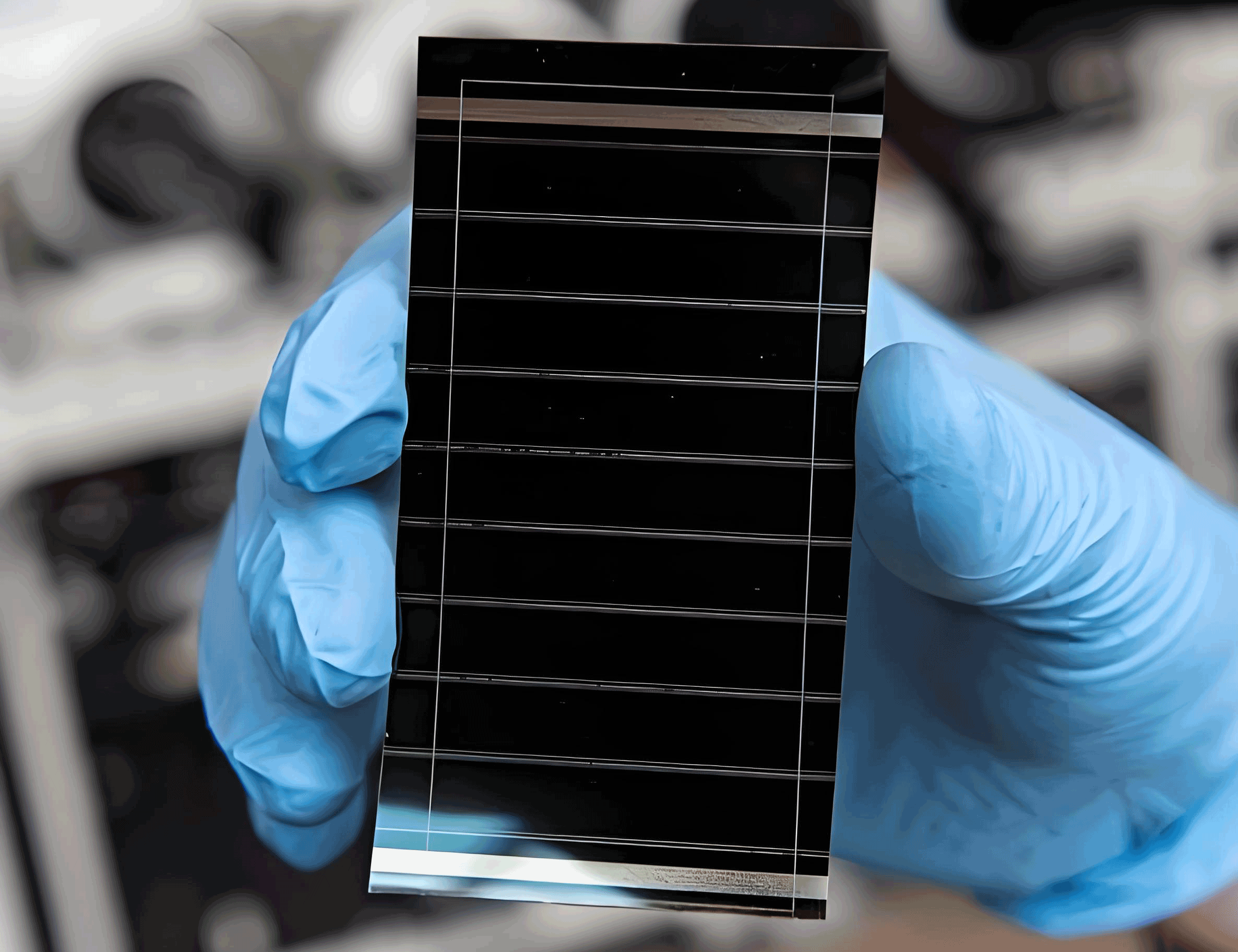
To begin, we fabricated the flexible tandem solar cell using a bottom-up process on a polyimide film, which offers excellent thermal stability and flexibility. The substrate was thoroughly cleaned, followed by the deposition of an ITO transparent electrode via magnetron sputtering. The silicon bottom cell was formed as an n-i-p structure using sputtering techniques, while the perovskite top cell was prepared via a two-step sequential deposition method. This involved spin-coating a PTAA hole transport layer, followed by a PbI2 precursor layer, and then immersing it in a MAI/PEA solution to form a high-quality perovskite film. Finally, a PC61BM electron transport layer was applied. A critical step was the low-power sputtering of the intermediate tunneling junction, where a MoO3/ITO bilayer structure was employed to ensure minimal optical and electrical losses. The entire device was encapsulated with UV-curable epoxy resin to enhance long-term stability, considering factors like material compatibility and interface optimization.
The crystallization quality of the perovskite film on the flexible substrate is crucial for the overall performance of the perovskite solar cell. We investigated the effects of varying the MAI/PEA mass ratio on the film’s structural and morphological properties. X-ray diffraction (XRD) analysis revealed distinct peaks at 14.2°, 28.5°, and 31.9°, corresponding to the (110), (220), and (310) crystal planes of CH3NH3PbI3 perovskite, respectively, indicating high crystallinity on the flexible polyimide substrate. By adjusting the MAI/PEA ratio, we controlled the grain size and defect density. Optimal results were achieved with a MAI/PEA mass ratio of 10:0.5, where the perovskite grains reached approximately 600 nm in size, and the grain boundary defect density was minimized. Scanning electron microscopy (SEM) images further confirmed that without PEA, the film exhibited irregular small grains with incomplete surface coverage; with an appropriate amount of PEA (10:0.5), grain growth and interface passivation were promoted, leading to a uniform and dense film; however, excess PEA (e.g., 10:1 or 10:2) resulted in the formation of excessive two-dimensional phases, reducing grain size and impairing charge transport.
The photoelectric performance of single-layer flexible perovskite solar cells was evaluated under standard AM 1.5G illumination, and the results are summarized in Table 1. The addition of PEA at a 10:0.5 ratio significantly improved the open-circuit voltage (Voc) and short-circuit current density (Jsc), primarily due to enhanced passivation of perovskite grain boundaries and superior film morphology, which reduced non-radiative recombination losses. Although higher PEA content could further increase Voc, it led to a decline in Jsc and fill factor (FF) owing to hindered charge transport. The optimized single-layer perovskite solar cell achieved an efficiency of 16.3%, approaching the performance levels observed on rigid substrates (typically around 17.5%). This underscores the importance of additive engineering in flexible perovskite solar cells to balance crystallinity and charge dynamics.
| MAI/PEA Mass Ratio | Open-Circuit Voltage (V) | Short-Circuit Current Density (mA/cm²) | Fill Factor (%) | Photoelectric Conversion Efficiency (%) |
|---|---|---|---|---|
| 10:0 | 1.02 | 20.1 | 72.5 | 14.8 |
| 10:0.5 | 1.07 | 20.8 | 73.2 | 16.3 |
| 10:1 | 1.09 | 19.5 | 72.8 | 15.4 |
| 10:2 | 1.10 | 18.3 | 71.6 | 14.4 |
For the silicon bottom cell, we focused on enhancing light absorption, particularly in the long-wavelength region, by optimizing the texture structure. A multi-scale approach was adopted, combining micron-scale random pyramids with nano-scale pillars to create a dual-layer texture. This design significantly reduced the average reflectance in the 550–1100 nm wavelength range from 35% to 7.5%, as confirmed by reflectance spectroscopy. The external quantum efficiency (EQE) measurements showed an improvement of approximately 30% in the 900–1000 nm range, indicating enhanced light trapping. The micron-scale pyramids primarily scatter incident light to minimize surface reflection, while the nano-pillars increase the interface light field intensity through resonant effects, collectively extending the optical path length within the silicon layer. As a result, the short-circuit current density of the flexible silicon solar cell increased from 15.2 mA/cm² to 18.7 mA/cm², representing a 23.5% enhancement. This optimization is critical for maximizing the current matching in the tandem configuration, as the silicon bottom cell must efficiently absorb photons that are transmitted through the perovskite top cell.
The interface between the perovskite and silicon subcells plays a pivotal role in the performance of the tandem solar cell. We evaluated different interface structures, including direct stacking without a tunneling junction, a single ITO layer, and a MoO3/ITO composite tunneling junction. Current-density-voltage (J-V) curves revealed that devices without a tunneling junction or with a single ITO layer exhibited severe S-shaped characteristics, indicating significant charge accumulation and transport barriers. In contrast, the MoO3/ITO composite structure demonstrated ideal photovoltaic behavior, with an open-circuit voltage of 1.72 V, close to the sum of the individual subcell voltages (1.07 V from the perovskite layer and 0.69 V from the silicon layer, totaling 1.76 V). This suggests that interface recombination losses were effectively suppressed. Contact resistance measurements further confirmed the superiority of the MoO3/ITO tunneling junction, with a resistance of only 2.3 Ω·cm², significantly lower than that of the single ITO layer (15.7 Ω·cm²). This reduction in series resistance contributed to a high fill factor of 73.5% in the tandem device, comparable to that of the single-layer perovskite solar cell.
Energy band analysis illustrated that MoO3, with its high work function (6.8 eV), facilitates effective valence band alignment, promoting efficient recombination of holes from the perovskite solar cell and electrons from the silicon solar cell. The ITO layer ensures good lateral conductivity and optical transparency. Atomic force microscopy (AFM) images showed that the 5 nm MoO3 and 40 nm ITO composite tunneling junction had a uniform and smooth surface, which is conducive to the growth of high-quality perovskite films on top. The performance parameters of the flexible perovskite-silicon tandem solar cells with different interface structures are compared in Table 2. The MoO3/ITO structure not only delivered the highest efficiency of 22.7% but also achieved better current matching, with a short-circuit current density of 18.0 mA/cm², closely aligning with the limiting current densities of the subcells (approximately 20.8 mA/cm² for the perovskite layer and 18.7 mA/cm² for the silicon layer). This optimization ensures balanced photocurrent generation and minimizes losses in the tandem configuration.
| Interface Structure | Open-Circuit Voltage (V) | Short-Circuit Current Density (mA/cm²) | Fill Factor (%) | Photoelectric Conversion Efficiency (%) |
|---|---|---|---|---|
| No Tunneling Junction | 1.36 | 17.9 | 52.8 | 12.8 |
| ITO Single Layer | 1.65 | 18.2 | 65.3 | 19.6 |
| MoO3/ITO Composite | 1.72 | 18.0 | 73.5 | 22.7 |
| MoO3/Au/ITO | 1.70 | 17.6 | 71.2 | 21.3 |
Mechanical and thermal stability are paramount for the practical deployment of flexible solar cells. We conducted bending tests with varying radii to assess mechanical durability. When the bending radius exceeded 10 mm, the device performance showed negligible degradation. However, at a radius of 5 mm, after 1,000 bending cycles, the efficiency decreased by only 8.2%, primarily due to slight reductions in fill factor and short-circuit current density. In contrast, at a smaller radius of 2 mm, performance deteriorated rapidly, with over 60% efficiency loss after just 50 cycles, attributed to ITO electrode cracking and perovskite layer fractures. Further analysis indicated that the perovskite top cell exhibited better flexibility under stress, while the silicon layer and electrode interfaces were more susceptible to damage, reflecting differences in Young’s modulus among the materials. To quantify this, we developed a model for efficiency degradation under bending conditions:
$$ \eta = \eta_0 \times \left[1 – \alpha \times \exp\left(-\frac{R}{R_0}\right)\right] $$
where \(\eta\) is the efficiency after bending, \(\eta_0\) is the initial efficiency, \(R\) is the bending radius, and \(\alpha\) and \(R_0\) are fitting parameters related to the material and structure. In our study, \(\alpha = 0.97\) and \(R_0 = 1.23\) mm. This model can predict performance changes under different bending conditions, aiding in the design of flexible photovoltaic devices for real-world applications.
Thermal stability was evaluated by exposing the devices to temperatures ranging from 25°C to 80°C. At 60°C, a typical operating temperature, the efficiency decreased from 22.7% to 20.9%, a reduction of approximately 7.9%, which is superior to conventional organic solar cells that often show around 15% degradation. Thermal infrared imaging confirmed uniform surface temperature distribution under simulated sunlight, with a maximum temperature of about 58°C and no observable hot spots, indicating good interfacial contact and even thermal stress distribution. The enhanced stability is largely attributed to the optimized material interfaces and the composite tunneling junction structure, which mitigate degradation mechanisms such as ion migration in the perovskite solar cell and delamination at the interfaces.
In summary, this study demonstrates a comprehensive optimization strategy for flexible perovskite-silicon tandem solar cells, addressing key challenges in crystallization, light management, and interface engineering. The use of PEA additive improved the perovskite film quality, the multi-scale texture enhanced silicon light absorption, and the MoO3/ITO tunneling junction enabled efficient electrical connection. The resulting device achieved a high efficiency of 22.7% with robust mechanical and thermal stability, making it suitable for applications in wearable electronics, portable charging systems, and building-integrated photovoltaics. Future work could focus on further scaling up the fabrication process and exploring alternative materials to push the boundaries of flexible perovskite solar cell technology. The insights gained here contribute to the ongoing advancement of high-performance, durable photovoltaic solutions for a sustainable energy future.