
As a connecting device between photovoltaic modules and the power grid, the performance of solar grid connected inverters has a significant impact on photovoltaic power generation systems. The current source grid connected inverter (CSGCI) uses an inductor as its DC side energy storage element. Compared to capacitors, the inductor has stable performance and can be used as an equivalent current source with a DC voltage power supply combined with a large inductor, allowing direct current to pass through on the bridge arm. Therefore, compared to voltage source solar inverters, it has higher safety and stability. Due to the characteristic of maintaining a constant current source, the AC side current and impedance of CSGCI are not related, but only related to the grid voltage and impedance. By changing the impedance value, the purpose of voltage control is achieved, and it has good boost performance. In addition, the output current of CSGCI can be directly fed into the power grid through a filter, without the need for additional devices for signal conversion. It has the advantages of fast response speed and low harmonic current in the power grid. Therefore, CSGCI is widely used in photovoltaic grid connected power generation, uninterrupted inverter power supply and other systems. The existing traditional bridge CSGCI has a simple structure and features such as unipolar modulation and three-level output. But when the switches connected to both sides of the current source are simultaneously disconnected, the charging path of the current will be blocked, and there will be a huge voltage peak between the switch tubes. Therefore, when switching switches with the same bridge arm, it is necessary to add overlapping time between the switches. The addition of overlapping time will introduce low-frequency harmonic components that are difficult to filter into the output current of CSGCI. And if the overlap time is set improperly, it may even cause serious distortion of the output current of CSGCI. In addition, the common mode voltage of traditional bridge CSGCI varies at high frequencies during the power cycle, resulting in significant common mode leakage current. According to the German VDE-0126-1-1 standard, when the maximum leakage current of the solar grid connected inverter is greater than 300 mA, the solar grid connected inverter needs to be disconnected from the grid within 0.3 seconds. In practical engineering, when traditional bridge type CSGCI is connected to the power grid, bulky isolation transformers need to be installed to suppress high-frequency common mode leakage current, which will directly increase the volume and cost of the traditional CSGCI system.
To address the shortcomings of existing CSGCI switches with the same bridge arm that require setting overlapping time and high common mode leakage current, a transformer less current source grid connected inverter with non overlapping time (TCSGCI-NT) is first proposed; Then analyze its modulation strategy, working mode, common mode leakage current, and mode conversion process; Finally, establish a hardware experimental platform for experimental verification.
1. No overlap time, no transformer, current source solar grid connected inverter
1.1 New TCSGCI-NT Circuit Topology
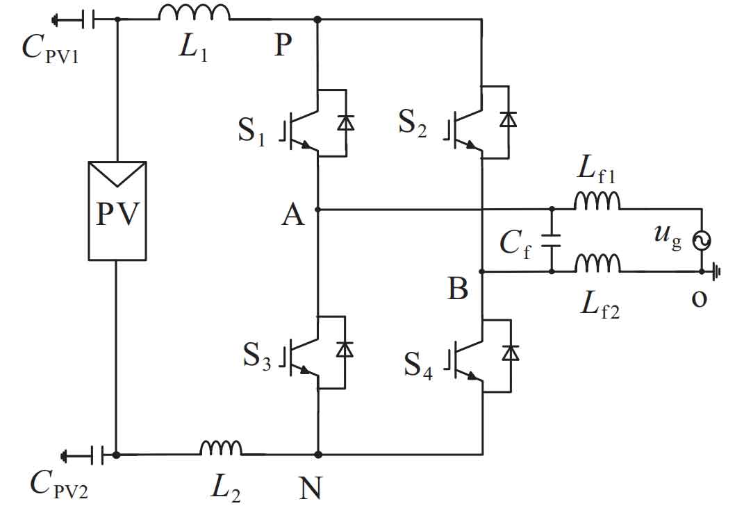
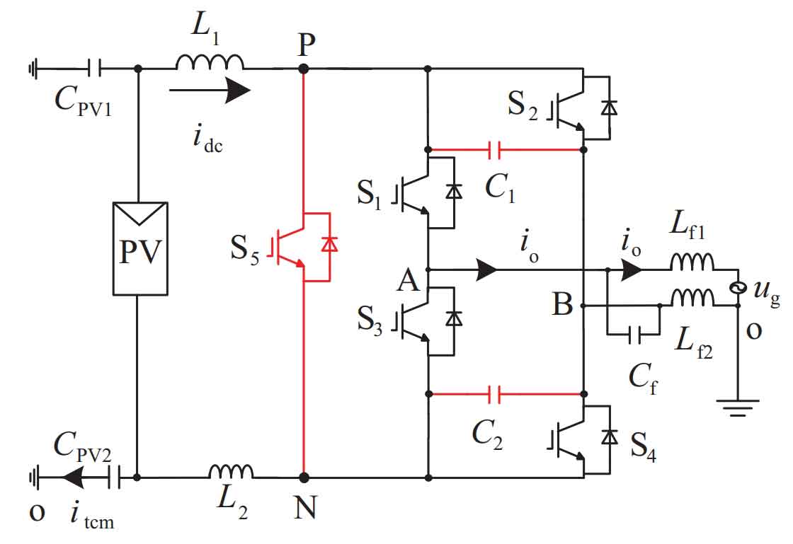
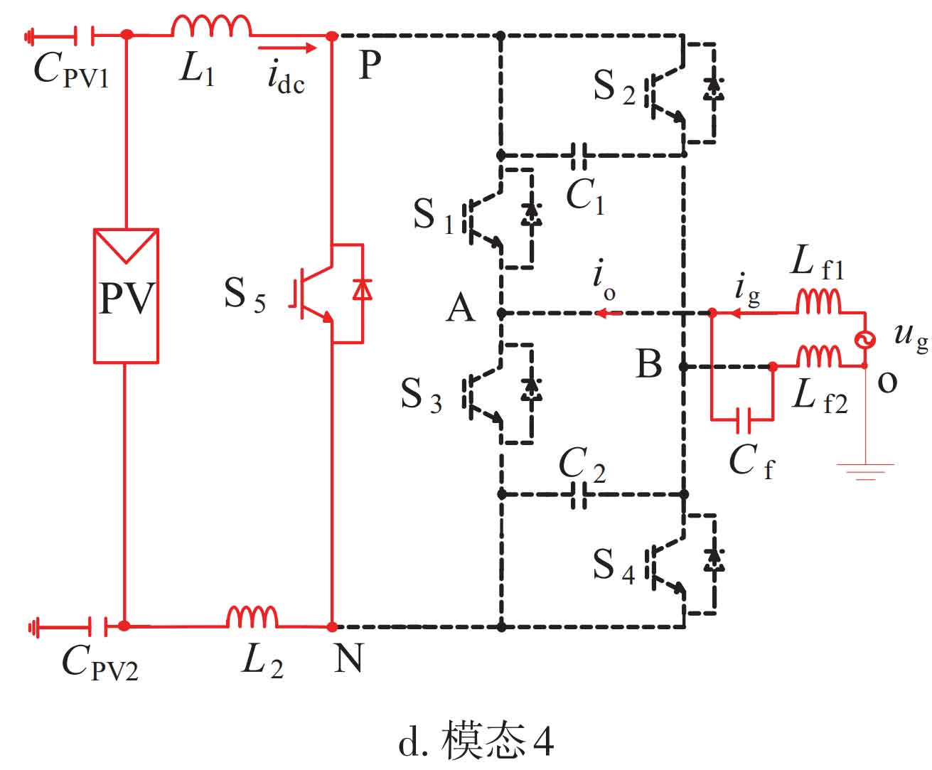
The typical structure of the existing traditional bridge type CSGCI is shown in Figure 1. An H5 bridge solar grid connected inverter with an additional switch on the DC side of the H-bridge solar grid connected inverter is proposed to effectively suppress the high-frequency common mode leakage current of the solar grid connected inverter. At the same time, in order to prevent significant voltage peaks on the switch tubes when the same bridge arm switch tubes are turned off simultaneously, two capacitors are introduced between the two bridge arms of the solar grid connected inverter. Based on the above ideas, on the basis of the traditional CSGCI topology, this paper proposes a new TCSGCI-NT topology by adding auxiliary circuits, as shown in Figure 2. In Figure 2, Cpv1 and Cpv2 represent the distributed capacitance of the positive terminal P and negative terminal N of the photovoltaic module’s DC voltage to ground, respectively, with O as the grounding point, where Cpv1=Cpv2=Cpv; S1~S4 are power switches for the inverter bridge of the TCSGCI-NT main circuit; S5 is an additional switch tube added between the DC side bridge arms; C1 and C2 are the two filtering capacitors introduced between the bridge arms; Lf1 and Lf2 are the filtering inductors on the AC side; L1 and L2 are energy storage inductors on the DC side, which can be used for energy storage; Cf is the filtering capacitor; Ug and ig are the grid connected voltage and current, respectively; Itcm is the common mode leakage current; IO is the output current of the bridge arm; IDC is the current of the DC side energy storage inductor.
1.2 Unipolar SPWM modulation method
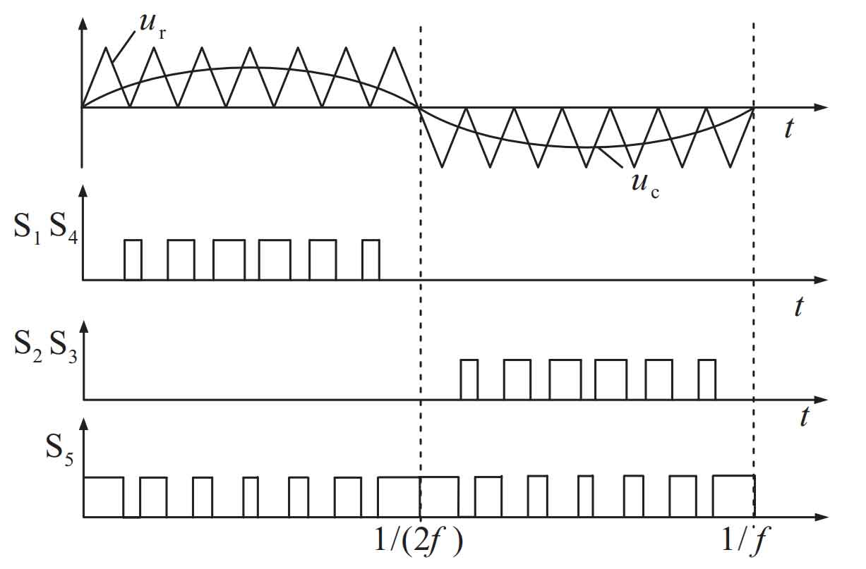
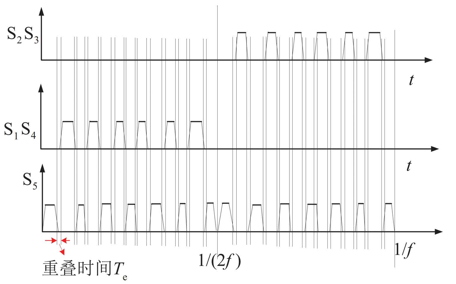
According to the TCSGCI-NT topology, a unipolar SPWM modulation strategy and its driving signals for S1~S5 are designed as shown in Figure 3. Where ur is the unipolar triangular carrier, uc is the modulation wave, and f is the grid frequency. When uc>0, ur is compared with uc to generate driving signals for S1 and S4, S2 and S3 remain turned off, S1=S4, S5=S1. When uc<0, comparing ur with uc generates driving signals for S2 and S3, S1 and S4 remain turned off, S2=S3, S5=S3.
Therefore, from the above analysis, it can be seen that TCSGCI-NT using half cycle modulation has only four high-frequency switches within half a power cycle, which can effectively reduce the switching loss of the solar inverter.
2. Working mode and common mode leakage current analysis
2.1 Common mode equivalent circuit
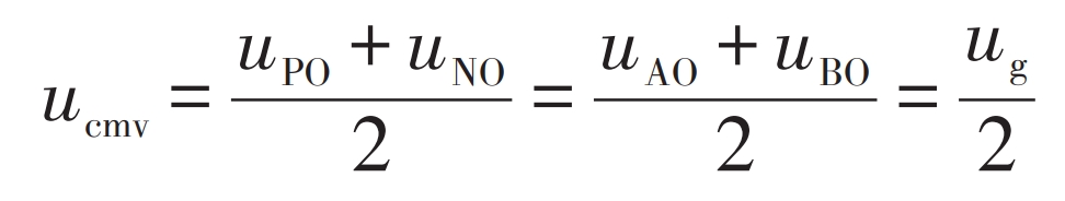
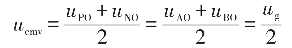
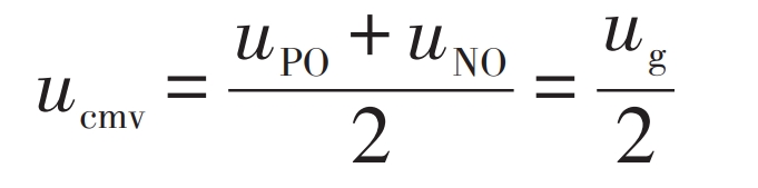
Let ig flow from the midpoint A of the bridge arm to B as positive. Due to the parallel relationship between the two parasitic capacitors, the equivalent capacitance size is 2Cpv. Cpv has the characteristic of alternating current isolation, so itcm is only related to AC power supply. To eliminate differential mode leakage current, set L1=L2=L. UPO and uNO are the voltages of the P-terminal and N-terminal to the ground O point, respectively. When ignoring the influence of DC current source on itcm, the common mode circuit equivalent model of TCSGCI-NT is shown in Figure 4.
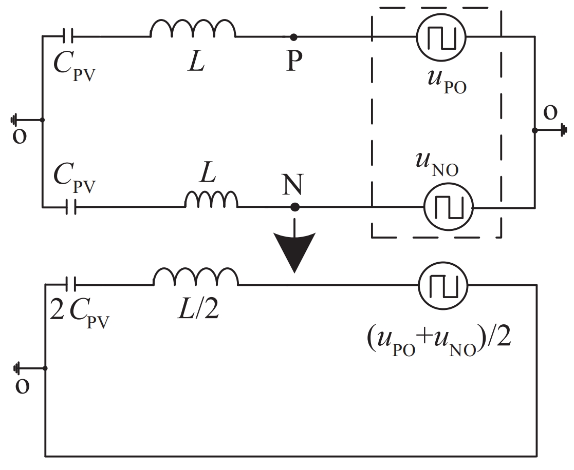
From Figure 4 and the formula, it can be seen that the itcm in the circuit is caused by the high-frequency variation of ucmv.
In the formula: ucmv – effective common mode voltage.
2.2 Working Mode and Analysis of High Frequency Common Mode Leakage Current
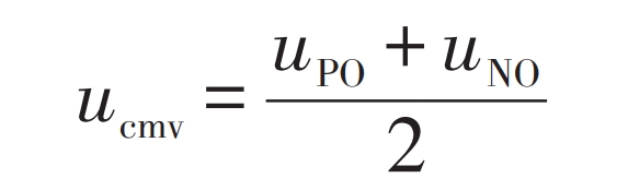
To analyze the high-frequency common mode leakage current of TCSGCI-NT in the positive and negative half cycles, when ig is positive from A to B. According to the switching conditions of S1~S5 in Figures 2 and 3, TCSGCI-NT can be divided into four operating modes, and their equivalent circuits are shown in Figures 5a~5d, respectively.
Mode 1: When ig>0, S1 and S4 are on, and S2, S3, and S5 are off, TCSGCI-NT operates in Mode 1, and its equivalent circuit is shown in Figure 5a. As shown in Figure 5a, the solar panels PV, L1, S1, Cf, S4, and L2 form a forward charging closed loop; At the same time, Lf1, ug, Lf2, and Cf form a forward charging system, providing forward power to ug. From Figure 5a, it can be seen that io=Idc, uPO=uAO=ug, uNO=uBO=0. Therefore, from equation (1), the ucmv of mode 1 can be obtained as:
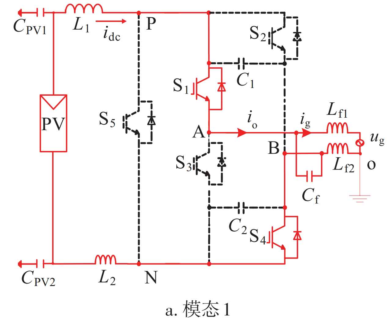
Mode 2: When ig>0, S5 is on, and S1, S2, S3, and S4 are off, TCSGCI-NT operates in Mode 2, and its equivalent circuit is shown in Figure 5b. From Figure 5b, it can be seen that the solar cells PV, L2, L1, and S5 form a forward DC side continuation circuit, while Lf1, ug, Lf2, and Cf form a forward discharge to supply power to ug. Io=0, according to KVL law and Figure 5b:
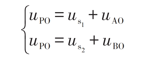
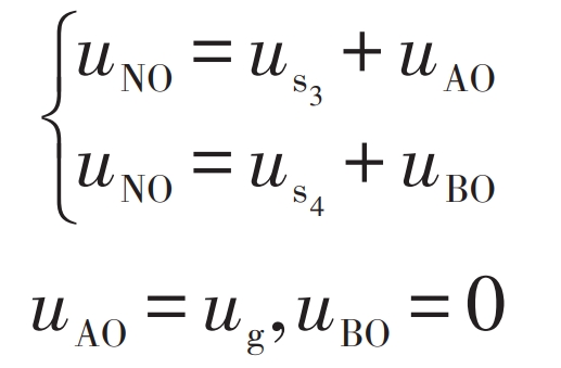
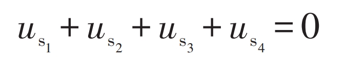
In the formula: us1, us2, us3, and us4- voltage stress of switch tubes S1, S2, S3, and S4.
According to KVL law and Figure 5b, it can be concluded that:
The simultaneous formula can obtain:
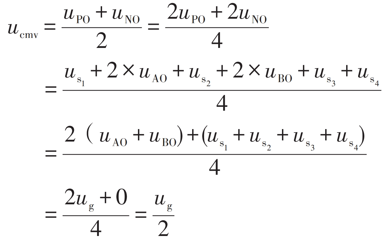
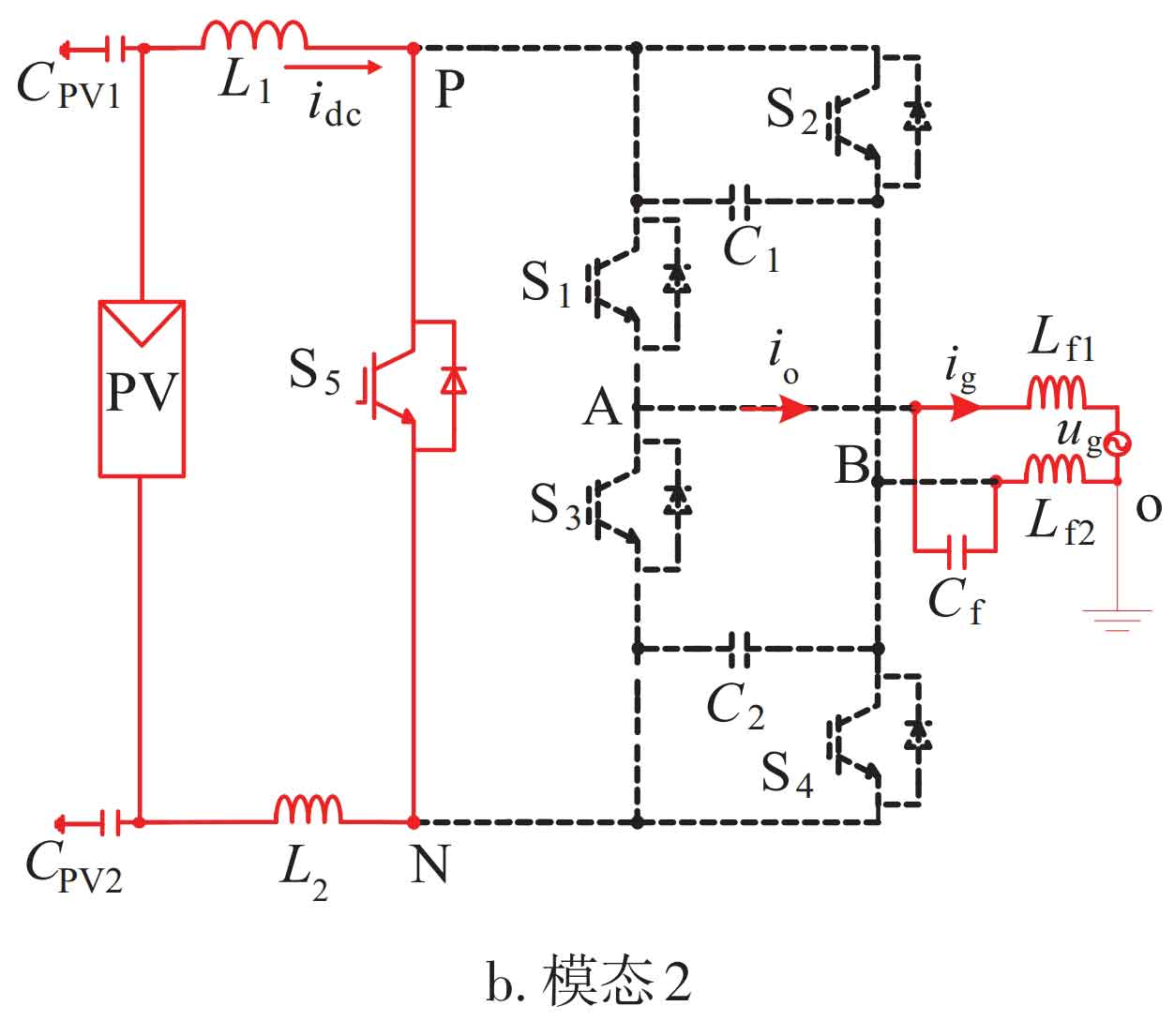
Mode 3: When ig<0, S2 and S3 are on, and S1, S4, and S5 are off, TCSGCI-NT operates in Mode 3, and its equivalent circuit is shown in Figure 5c. From Figure 5c, it can be seen that the solar cells PV, L1, S2, Cf, S3, and L2 form a forward charging closed loop; At the same time, Lf1, ug, Lf2, and Cf form a reverse charging system, providing reverse power to ug. From Figure 5c, it can be seen that io=- Idc, uPO=uBO=0, uNO=uAO=ug. Therefore, according to the formula, the ucmv of Mode 3 can be obtained as:
Mode 4: When ig<0, S5 is on, and S1, S2, S3, and S4 are off, TCSGCI-NT operates in Mode 4, and its equivalent circuit is shown in Figure 5d. From Figure 5d, it can be seen that the solar cells PV, L1, L2, and S5 form a negative DC side continuous current circuit, while Lf1, ug, Lf2, and Cf form a forward discharge, providing negative power to ug. Similar to Mode 2, i0=0 can be obtained, and the ucmv of Mode 4 is:
From the above, the switch status and ucmv of TCSGCI-NT are shown in Table 1.
| Modal | S1=S4 | S2=S3 | io | S5 | ucmv |
| 1 | 1 | 0 | Idc | 0 | 0.5ug |
| 2 | 0 | 0 | 0 | 1 | 0.5ug |
| 3 | 0 | 1 | -Idc | 0 | 0.5ug |
| 4 | 0 | 0 | 0 | 1 | 0.5ug |
From Table 1, it can be seen that modes 1 to 4 have the same ucmv ≈ 0.5ug, and the common mode voltage only contains low-frequency grid components, without high-frequency components. Therefore, the TCSGCI-NT topology and its unipolar modulation strategy proposed in this article can achieve three-level output current while effectively suppressing high-frequency common mode leakage current in solar inverter systems.
3. Analysis of Mode Transition Process
In an ideal situation, during the positive half cycle, the complementary driving signal S5 of the inverter circuit will not turn off simultaneously with S1 and S3, that is, the opening and closing actions will not have a delay after the control signal is sent. However, in practice, the on and off of the switch cannot be completed instantaneously, as shown in Figure 6.
During the process of converting from mode 1 to mode 2, S5, S1, and S3 will simultaneously turn off, causing the CSGCI inductance current to be unable to complete the continuous flow, resulting in a huge voltage peak on the switch tube, causing inverter failure and device burnout. Therefore, it is necessary to delay the triggering time of S5’s shutdown for a certain period of time, which is called the overlap time Te. This ensures that after S1 and S3 are reliably opened, S5 will be shut down again to ensure the smooth completion of the commutation process. The addition of overlapping time will introduce low-frequency harmonic components that are difficult to filter into the grid connected current of CSGCI. In addition, if the overlap time is set improperly, it may even cause serious distortion of the output current of CSGCI, making it difficult to meet the voltage and power quality requirements of photovoltaic power generation. This article introduces two capacitors C1 and C2 between the two bridge arms of the solar inverter. When S5 has been turned off and S2 and S3 have not yet been turned on, it is necessary to set the overlapping time period. The TCSGCI-NT equivalent circuit is shown in Figure 7. At this point, the photovoltaic current sources PV, L1, C1, C2, and L2 form an inductive current continuation loop within the overlapping time period, allowing the TCSGCI-NT inductive current to smoothly complete the continuation, and there will be no significant voltage peaks on the switch tube. Therefore, during the mode conversion process, TCSGCI-NT will successfully complete the commutation without setting the overlap time.
Similarly, the commutation process of TCSGCI-NT negative half cycle mode 3 and mode 4 can be analyzed. The commutation equivalent circuit is shown in Figure 7, and its analysis is the same as that of positive half cycle. Therefore, the TCSGCI-NT topology proposed in this article introduces a filtering capacitor between the two switch tubes of the two bridge arms to prevent CSGCI from opening, which has the advantage of not needing to set overlapping time.
4. Experimental verification
To verify the correctness of TCSGCI-NT topology and common mode leakage current analysis, a hardware experimental platform was established. The switch tube selection model is FGH40N60SFD, and the diode model is DSEI30-20A; The control core chip adopts a DSP model of TMS320F2812. The system experimental parameters are shown in Table 2, with Pout as the output power.
| Parameter | Value |
| Idc/A | 10.5 |
| Um/V | 220 |
| Cf/μF | 80 |
| f/Hz | 50 |
| fs/kHz | 5 |
| CPV/nF | 75 |
| L1=L2/mH | 8 |
| Lf1=Lf2/μH | 2.5 |
| Iref/A | 10 |
| Pout/W | 770 |
To achieve stable inverter grid connection of TCSGCI-NT, TCSGCI-NT adopts a direct current control strategy as shown in Figure 8. Using a phase-locked loop circuit (PLL) to obtain the initial phase angle of ug θ , Calculate sin based on the sine table in the program θ , Where iref=Im × Sin( ω T+ θ), Iref is the reference current of ig, and Im is the amplitude of iref. After subtracting ig from iref, uc is obtained through PI controller, and uc generates TCSGCI-NT circuit S1~S5 driving signals through unipolar SPWM modulation.
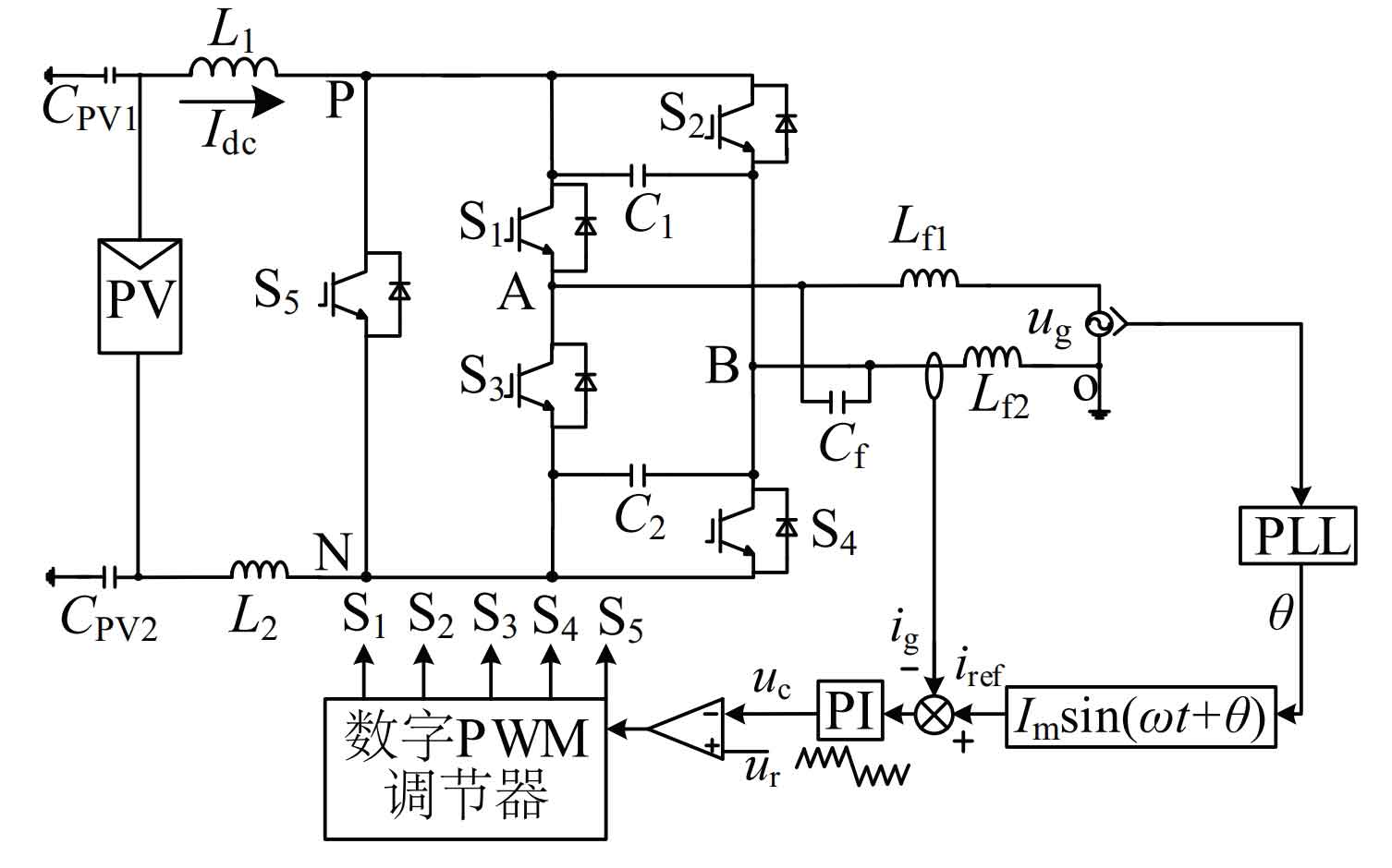
Figure 9a shows the waveform of idc, which remains at 10.5 A. Figure 9b shows the waveforms of ug and ig, indicating that ug and ig remain in phase. The amplitude of ug is approximately 220 V, and the amplitude of ig is approximately 10 A. Figure 9c shows the waveform of ig and its FFT analysis, indicating that the frequency of ig is mainly distributed at the fundamental frequency of 50 Hz and the switching frequency of 5 kHz, with fewer harmonics. Therefore, the TCSGCI-NT and its controller proposed in this article can achieve stable inversion, and the system has high power factor and power quality.
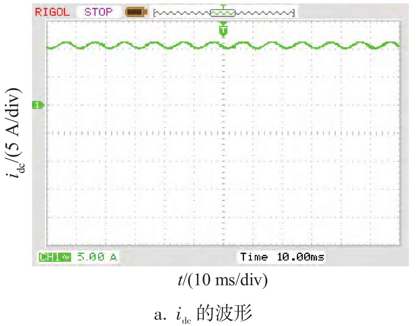
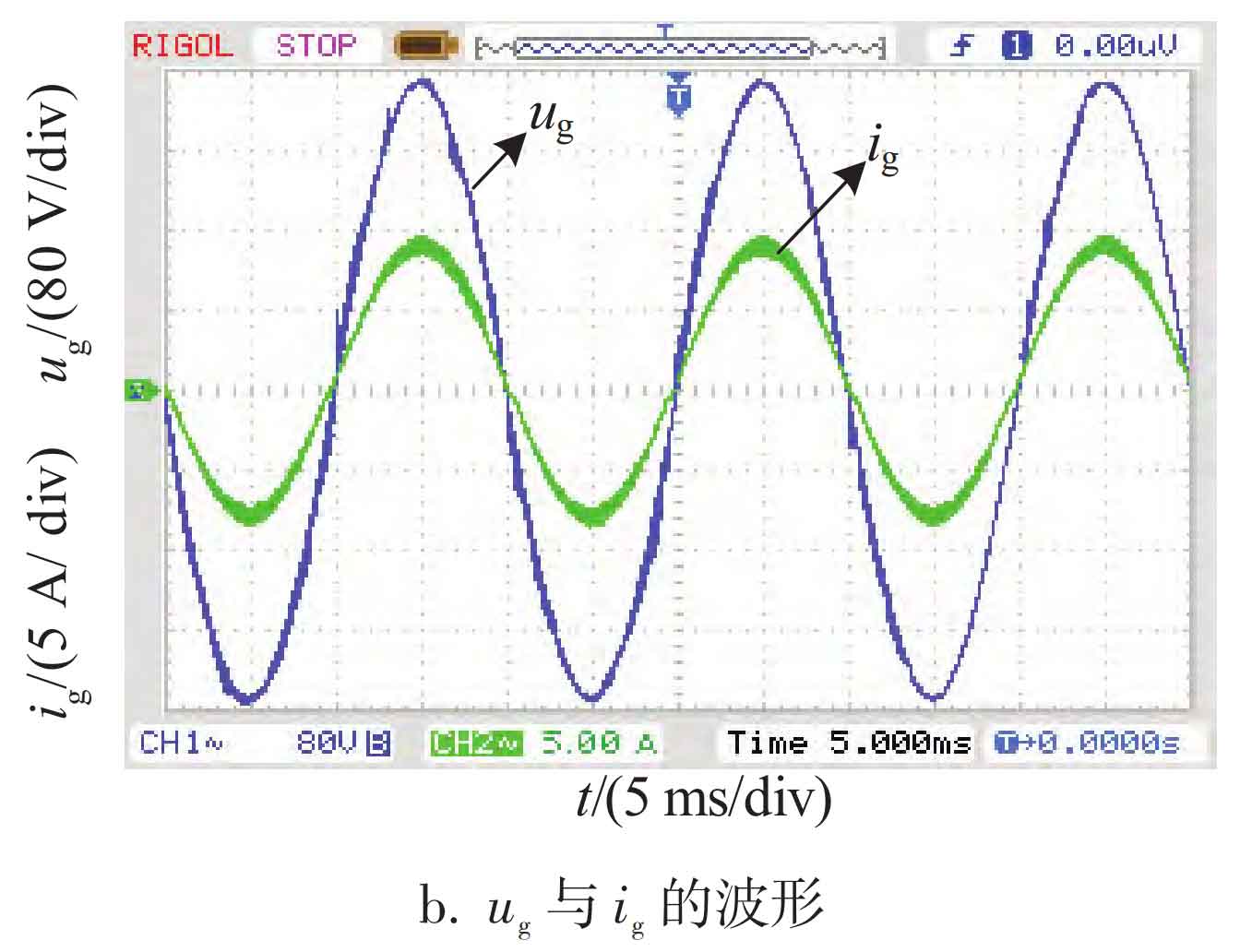
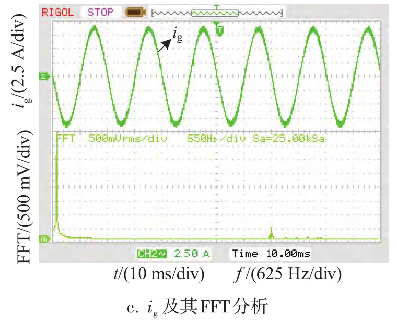
Figure 10 shows the waveforms of uPO, uNO, and uPO+uNO. From Figure 10, it can be seen that the peak value of uPO+uNO is about 220 V, so ucmv=(uPO+uNO)/2, ucmv ≈ ug/2. The frequency of uPO+uNO is about 50 Hz, only containing low-frequency components and not high-frequency components.
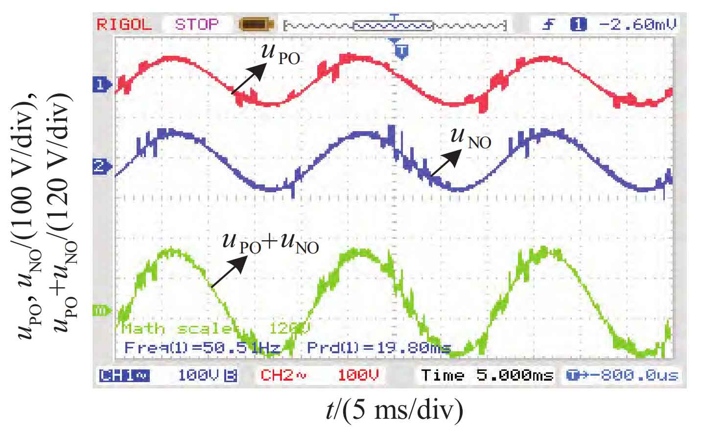
Figure 11 shows the waveform of the voltage UPV and itcm on the distributed capacitor CPV. From Figure 11, it can be seen that UPV ≈ ug/2 ≈ ucmv does not include high-frequency components, and the amplitude of itcm is about 20 mA.
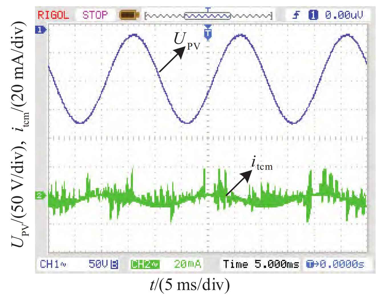
In summary, the leakage current of TCSGCI-NT has been effectively suppressed, meeting the requirements of VDE-0126-1-1 standard for the leakage current of solar grid connected inverters.
5. Conclusion
Through the study of the TCSGCI-NT topology and its common mode leakage current proposed in this article, it can be concluded that:
1) The TCSGCI-NT topology introduces a filtering capacitor between the two switch tubes of the two bridge arms to prevent the current mode GCI from opening. During the mode conversion process, TCSGCI-NT will be able to successfully complete commutation without the need to set an overlap time.
2) The provided unipolar SPWM modulation method puts the switch in a half cycle operating mode, reduces switching losses, and outputs a three-level current. Moreover, as there is no need to set overlap time, the output current harmonics of the inverter are small, so TCSGCI NT has high power quality.
3) The TCSGCI-NT freewheeling circuit does not pass through poor performance body diodes, so TCSGCI-NT has the advantage of high reliability.
4) The given half cycle modulation method maintains the common mode voltage ucmv of TCSGCI-NT modes 1-4 at ug/2, without high-frequency components. Without the need for isolation transformers, the common mode leakage current of TCSGCI-NT was effectively suppressed, with an amplitude of only about 20 mA.