
AC power can be divided into two types: Voltage Source Inverter (VSI) and Current Source Inverter (CSI). VSI dominates due to its low cost, simple control, and mature technology, and is widely used in photovoltaic systems. VSI, as the most important connecting device in photovoltaic grid connection, can be divided into two categories: isolated and non isolated. Its performance directly affects the efficiency and safety stability of photovoltaic power generation systems. Isolation type VSI grid connected inverter can achieve isolation between the input end and the grid side, improving safety performance. However, the presence of transformers can reduce the efficiency of the power generation system and increase costs. Therefore, non isolated solar photovoltaic inverters without transformers have become a hot research topic for scholars at home and abroad.
The non isolated solar photovoltaic grid connected inverter, due to the lack of electrical isolation, causes the high-frequency common mode voltage (CMV) caused by the high-frequency switch to act on the stray capacitance of the PV array, generating a large common mode leakage current. According to the VDE-0126-1-1 standard, when the leakage current is higher than 0.3 A, the solar photovoltaic inverter needs to be disconnected from the grid within 0.3 seconds. In this regard, reference studied a clamp type solar photovoltaic inverter topology based on a half bridge circuit. This structure directly connects the neutral point of the power grid to the midpoint of the DC side divider capacitor, keeping the voltage at both ends of the parasitic capacitor of the photovoltaic array unchanged and suppressing leakage current. Although it meets the VDE-0126-1-1 standard, the challenge it faces is the low utilization rate of the DC side voltage. A three-level Neutral Point Clamped (NPC) inverter was studied, with the same principle as above. However, there is a double power frequency fluctuation in the midpoint potential, resulting in a higher content of low order harmonics in the output current. In response to the above situation, domestic and foreign scholars have proposed widely adopted H5 topology, H6 topology, HERIC topology, and corresponding improved topology based on half bridge and H-bridge, with peak leakage inductance current all within 150 mA. The design concept of this type of topology is to decouple the DC and AC sides during the freewheeling phase, removing the leakage current transmission path. However, due to the presence of switch junction capacitors, this scheme cannot completely cut off the current path, so the leakage current still exists. Meanwhile, in the 2011 update of the standards for solar photovoltaic grid connected inverters, Germany proposed that distributed power generation systems should have reactive power support capabilities, which none of the above solutions have.
In recent years, the common ground topology is a theoretical solution that can completely eliminate leakage current. Its basic idea is to connect the negative terminal of the photovoltaic side to the neutral point of the power grid, and through equivalent circuits, it can be known that the stray capacitance is short circuited. Based on this, a common ground topology based on virtual DC bus structure was studied, but due to the absence of a charging circuit in the negative half cycle of the grid voltage, the waveform of the output current in the negative half cycle was distorted. A type of common ground two-level inverter is proposed, however, the use of bipolar sine pulse width modulation (SPWM) results in higher grid connected current harmonics, requiring a larger volume of filtering inductance, reducing power density and increasing manufacturing costs. In this regard, the topology of a multi-level common ground inverter has been studied, but the two bus capacitors do not have the ability to equalize voltage, which can cause serious distortion of the output waveform. References integrate the advantages of dual grounding topology, but high redundancy of semiconductor devices can lead to complex control strategies and difficulty in mass production. In this regard, a five level dual grounding topology with a flying capacitor structure as the basic unit is proposed, and the number of devices is significantly reduced. However, the above solutions are compatible with photovoltaic cells that are more sensitive to environmental changes, and there are also many new challenges, such as whether they have high voltage gain, reactive power compensation, low output current distortion, and other characteristics.
In summary, a novel non isolated common ground multi-level solar photovoltaic grid connected inverter was studied. This topology introduces a switched capacitor network based on the Boost circuit, where two capacitors have voltage self balancing ability, which can effectively avoid output current distortion. At the same time, the negative pole on the DC side is connected to the neutral point on the grid side, which theoretically can completely eliminate the common mode leakage current caused by stray capacitance to the ground, and has the ability to boost and support reactive power. This article provides a detailed analysis of the various operating modes of solar photovoltaic inverters, adopts a feedforward space vector modulation strategy, and compares the leakage current suppression ability with traditional H5 and HERIC topologies under the same parameters. Finally, a 1 kW experimental prototype was built to verify the correctness and effectiveness of the proposed solar photovoltaic inverter topology.
1. New topology and modal analysis
1.1 New topology structure
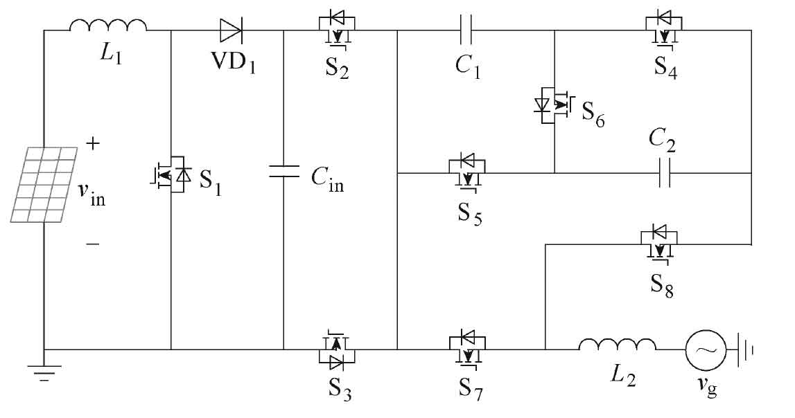
This paper proposes a novel five level non isolated solar photovoltaic inverter to address the issue of leakage current and harmonic interference. The proposed five level topology structure is shown in Figure 1, which consists of a photovoltaic array, 8 switching tubes S1-S8, 1 diode VD1, 3 capacitors Cin, C1, C2, and a filter. The proposed solar photovoltaic inverter integrates functions to enable the Boost circuit to provide high gain for output voltage while eliminating electrolytic capacitors used for power decoupling. In addition, two switching capacitor units can achieve self voltage equalization, and theoretically, the output voltage waveform is distortion free.
1.2 Working principle of new topology
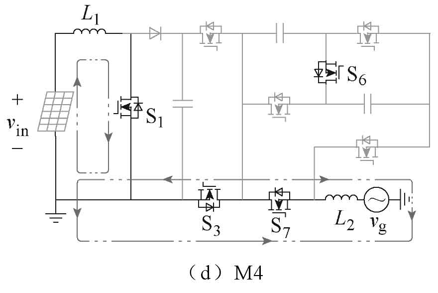
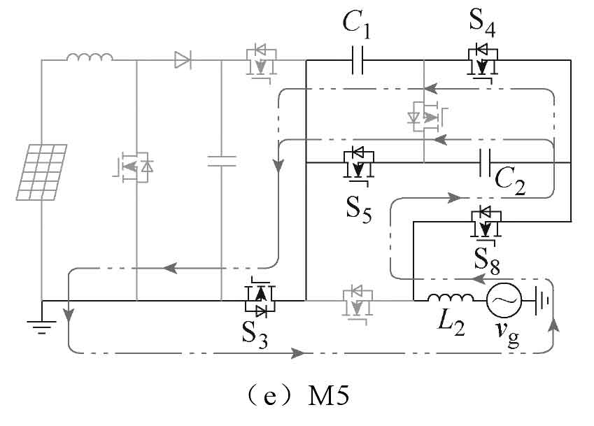
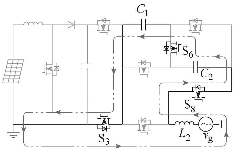
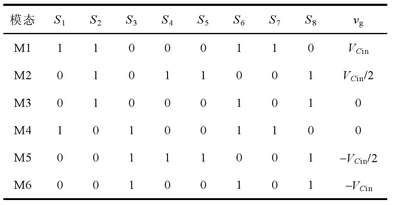
The new non isolated five level single-phase solar photovoltaic grid connected inverter has six operating modes, and its current path is shown in Figure 2. The output voltage of the photovoltaic panel is the voltage VC at both ends of the capacitor Cin. Table 1 shows the switching states of 8 switching tubes in 6 operating modes M1~M6, as well as the output voltage vg of the new solar photovoltaic inverter in each mode. In Table 1, Si represents the switching state and i represents the i-th switching tube. The driving signals of S1 and S7, S4 and S5 are the same; Meanwhile, the driving signals of S2 and S3, S5 and S6, S7 and S8 complement each other.
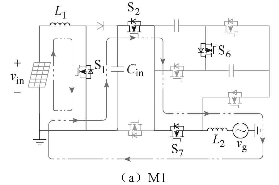
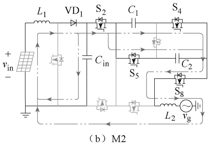
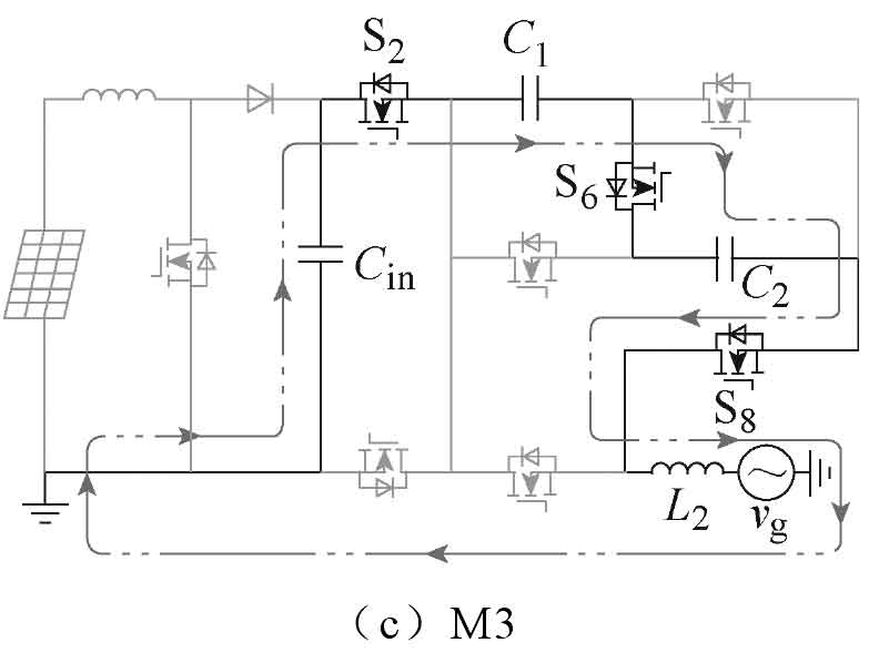
To simplify the analysis, in Figure 2, the mode of the switch tube S6 conducting but not forming a path is analyzed as a turn off. Assuming that the conduction voltage drop of the switching transistor and its anti parallel diode are the same and are VON-S and VON-VD, respectively. The detailed modal description is as follows:
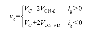
(1) M1: Switching tubes S1, S2, and S7 conduct, forming two closed circuits, namely the left boost circuit and the right inverter output circuit, as shown in Figure 2a. If the device voltage drop is considered, the output voltage and polarity of the output current of the solar photovoltaic inverter are:
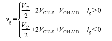
(2) M2: The switching tubes S2, S4, S5, and S8 conduct, and the capacitors C1 and C2 achieve voltage self balancing while maintaining VC/2, as shown in Figure 2b. At this point, if the device voltage drop is considered, the polarity of the output voltage and output current of the solar photovoltaic inverter is:
(3) M3: Switching tubes S2, S6, and S8 are conducting, and capacitor Cin simultaneously discharges capacitors C1 and C2. The current path is shown in Figure 2c. If considering the device voltage drop, the output voltage and current polarity of the solar photovoltaic inverter are:
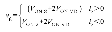
(4) M4: The switch tubes S1, S3, and S7 are conductive, forming a freewheeling circuit, as shown in Figure 2d. If considering the device voltage drop, the output voltage and current polarity of the solar photovoltaic inverter are:
(5) M5: Switch tubes S3, S4, S5, and S8 conduct, capacitors C1 and C2 complete voltage self balancing, and output in parallel, as shown in Figure 2e. If considering the device voltage drop, the output voltage and current polarity of the solar photovoltaic inverter are:
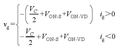
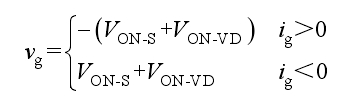
(6) M6: Switch tubes S3, S6, and S8 are conducting, and capacitors C1 and C2 are output in series. The flow path is shown in Figure 2f. If considering the device voltage drop, the output voltage and current polarity of the solar photovoltaic inverter are:
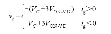
From the above modal analysis, it can be seen that switches S4 and S5 control capacitors C1 and C2 in two states of charging and discharging. From Table 1, it can be seen that the switch state is synchronous, therefore, the voltage at both ends of capacitors C1 and C2 is bound to be the same. In addition, each switch state can simultaneously achieve positive and negative current output, thus enabling reactive power feedback to the grid.
2. Control unit design
2.1 Feedforward space vector modulation strategy
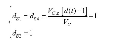
The traditional SV scheme is based on VC1=VC2=VC=VCin to design modulation strategies. However, in practice, it is impossible to choose the capacitance value of the switching capacitor as infinite. Therefore, there are three relationships: VC=1/2VCin, VC>1/2VCin, and VC<1/2VCin. The relationship between non ideal capacitor voltage and switch vector position is shown in Figure 3. For the convenience of analysis, Figure 3 is divided into four regions: R1, R2, R3, and R4.

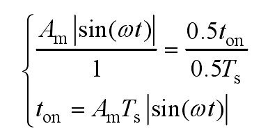
In view of this, the modulation strategy proposed in this article has two purposes: ① to provide a five level stepped wave for the output end; ② Decouple the output voltage from the fluctuating capacitor voltage to avoid output voltage distortion. Firstly, the reference voltage for sinusoidal output is defined as vg ref (t), with a duty cycle of d (t). The relationship between the two is:
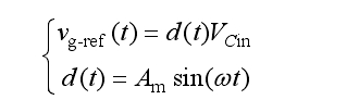
In the formula, Am is the modulation coefficient.
Under the reference voltage, the duty cycle of two adjacent space vectors is:
In the formula, VM and VN are the output voltages of adjacent switch vectors.
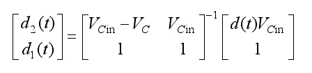
Assuming the output reference voltage is in the R4 region and considering the impact of capacitor voltage ripple on the output, the duty cycle of the control vector in M1 and M2 is:
According to the formula and Figure 4f, the duty cycles of switch tubes S1, S2, and S4 are:
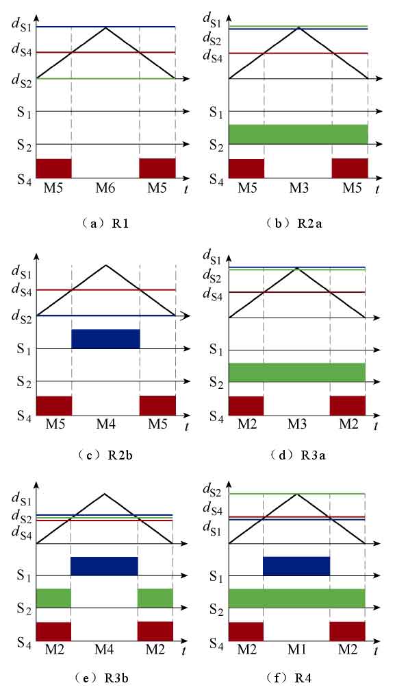
Similarly, Table 2 provides the duty cycle of the switch tubes in the remaining three regions under the feedforward space vector modulation strategy. Therefore, once the proposed modulation strategy detects the voltage of the switching capacitor, the vector position can be determined to decouple the disturbance from the voltage of the switching capacitor.
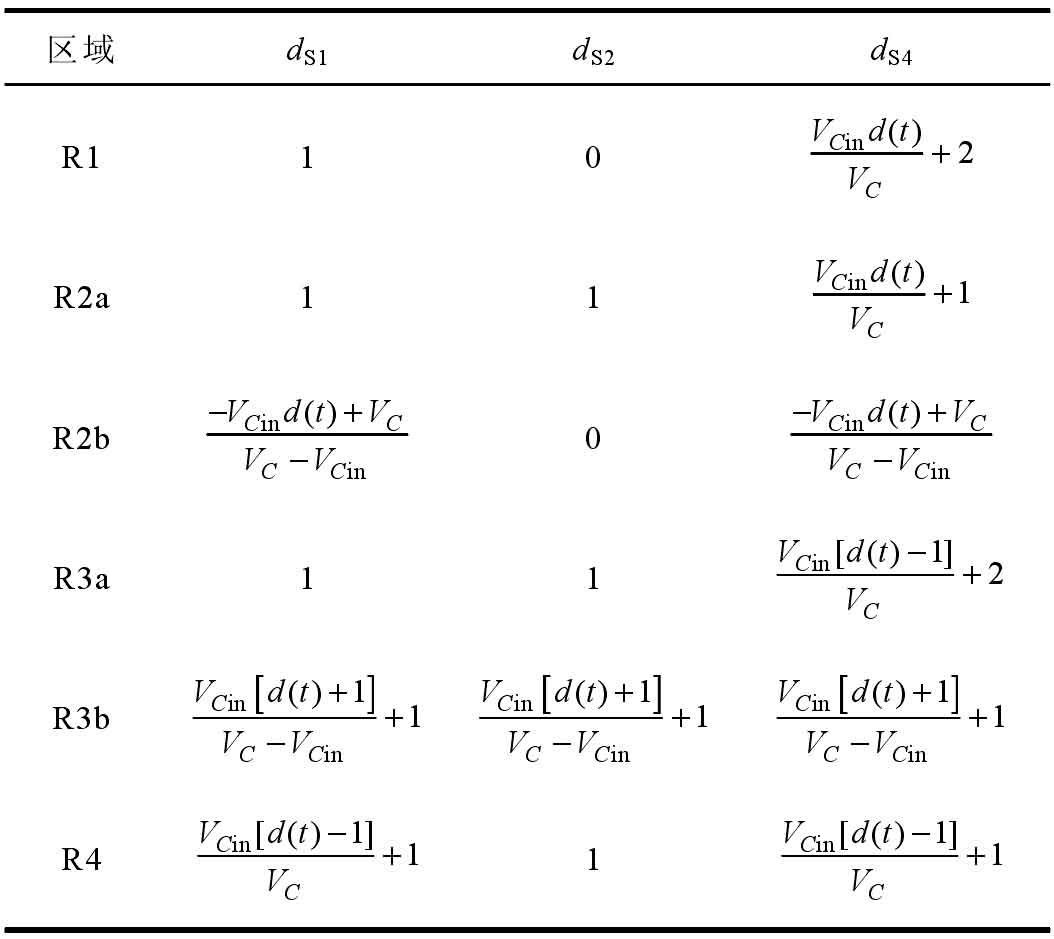
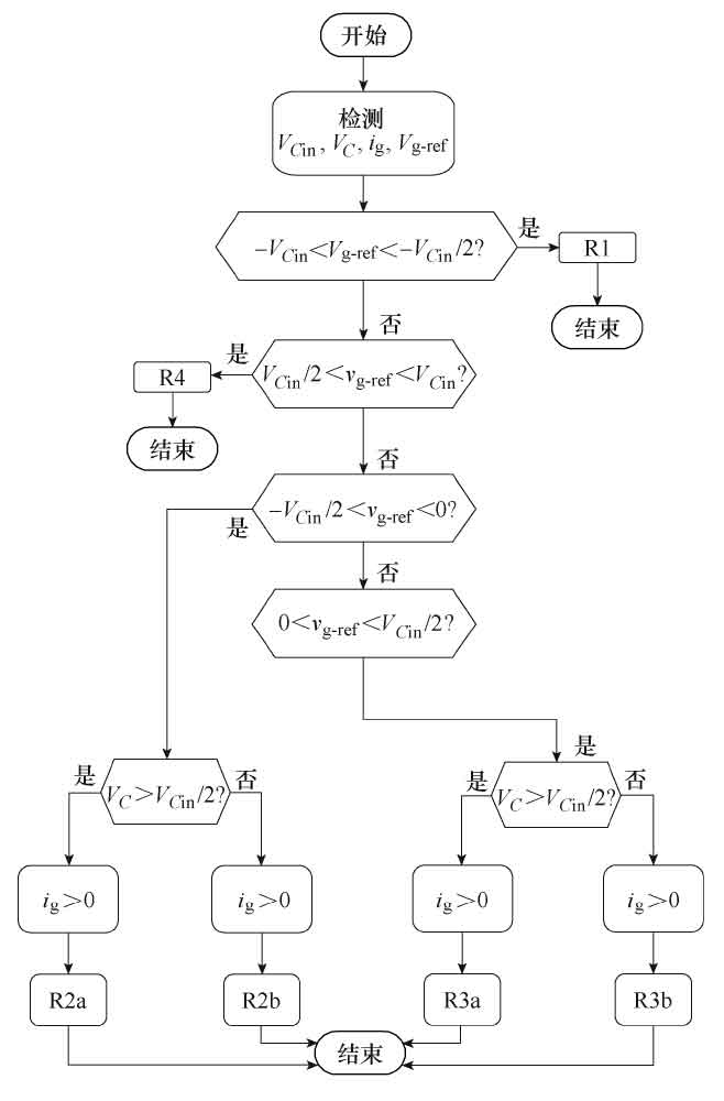
Figure 4 shows the switch sequence for all regions. The comparison logic of switch S1 is high level, and the comparison logic of S2 and S4 is low level. The proposed space vector modulation scheme can be generated in SV modulators with simple modulation signals and carrier signals. In order to minimize the harmonic distortion of the output voltage, Figure 5 shows the region selection block diagram in this paper. Each region is selected from redundant pairs R2a, R2b, and R3a, R3b based on input voltage error and output current signals.
2.2 Control Strategy
Figure 6 shows the control block diagram of the solar photovoltaic grid connected inverter for this design. This section includes PI controller, PR controller, and Phase Locked Loop (PLL). Firstly, input the reference voltage vin ref and compare it with the actual input voltage vin to obtain the error signal and transmit it to the next level. The signal enters the next level PI controller and obtains the peak reference value is-p-ref of the output current. At the same time, the PLL detects the phase and frequency of the power grid, and the two parts obtain the current reference signal is-ref that is in the same phase as the power grid voltage through a multiplier. Finally, the current controller adopts PR control to track the grid connected reference current. The transfer functions of the two controllers are:
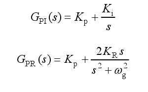
In the formula, Kp is the proportional gain; Ki is the integral gain; KR is the resonant gain; ω G is the resonant frequency.
3. Performance analysis
3.1 Common mode current
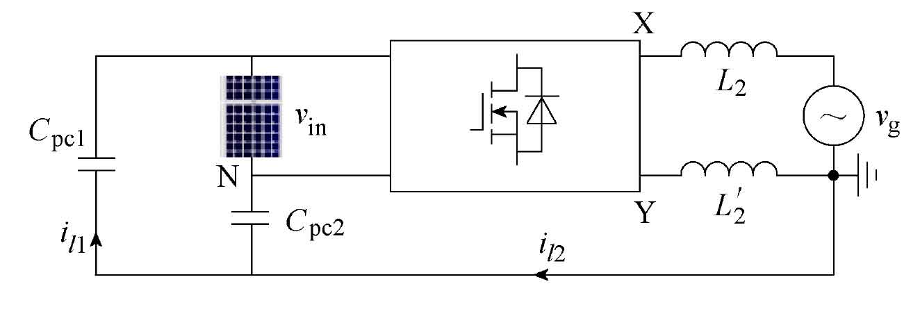
Figure 7 shows an equivalent simplified model of a traditional non isolated solar photovoltaic inverter with parasitic capacitance. From the graph, it can be seen that the common mode voltage VCM and the differential mode voltage VDM can be represented as:
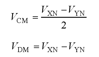
In the formula, VXN represents the voltage across X and N; VYN represents the voltage across Y and N.
It is known that VDM also has an impact on leakage current, so the total mode voltage VTCM can be expressed as:
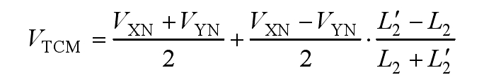
According to Figure 1, 2L ′=0. Therefore, the formula can be simplified as:
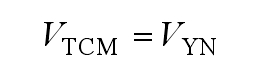
At this point, the common mode current on the parasitic capacitor is:
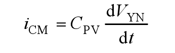
According to the formula, the magnitude of leakage current is affected by the amplitude and frequency of the equivalent common mode current voltage VTCM variation. The proposed solar photovoltaic inverter topology benefits from the common ground structure VYN=0, thus the new topology has the ability to completely eliminate leakage current.
3.2 Gain Analysis
According to modal analysis and the principle of volt second balance, it can be concluded that:
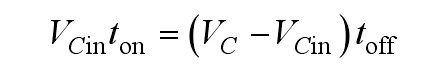
In the formula, ton is the time for the switching tube S1 to conduct; Toff is the time of shutdown.
Ignoring component losses, according to the principle of energy conservation, it can be concluded that:
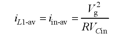
In the formula, iL1 av is the average current of inductance L1; Iin-av is the average current of the output current; Vg is the effective value of the output voltage; R is a resistive load.
Furthermore, it can be concluded that:
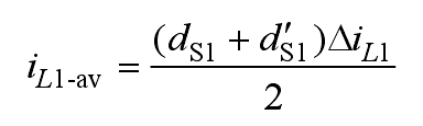
In the formula, Δ IL1=VCindS1Ts/L1, dS1Ts is the time it takes for the inductive circuit iL1 to decrease from its maximum value to zero, and Ts is the switching cycle; S1d and S1d ‘are the on/off ratio and on/off ratio of the switch, respectively.
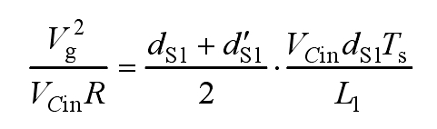
The simultaneous formula yields:
By using the rule sampling method and utilizing the principle of similar triangles, it can be concluded that:
The joint formula yields the effective value expressions for dS1 and S1d ‘, which are:
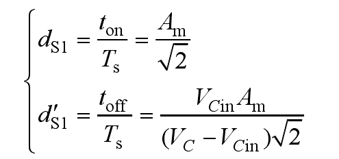
The relationship between the output voltage of the solar photovoltaic inverter and the voltage and duty cycle of the bus capacitor is known as dS1VC=Vg, and the following formula can be obtained:
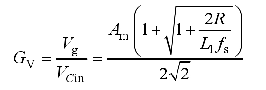
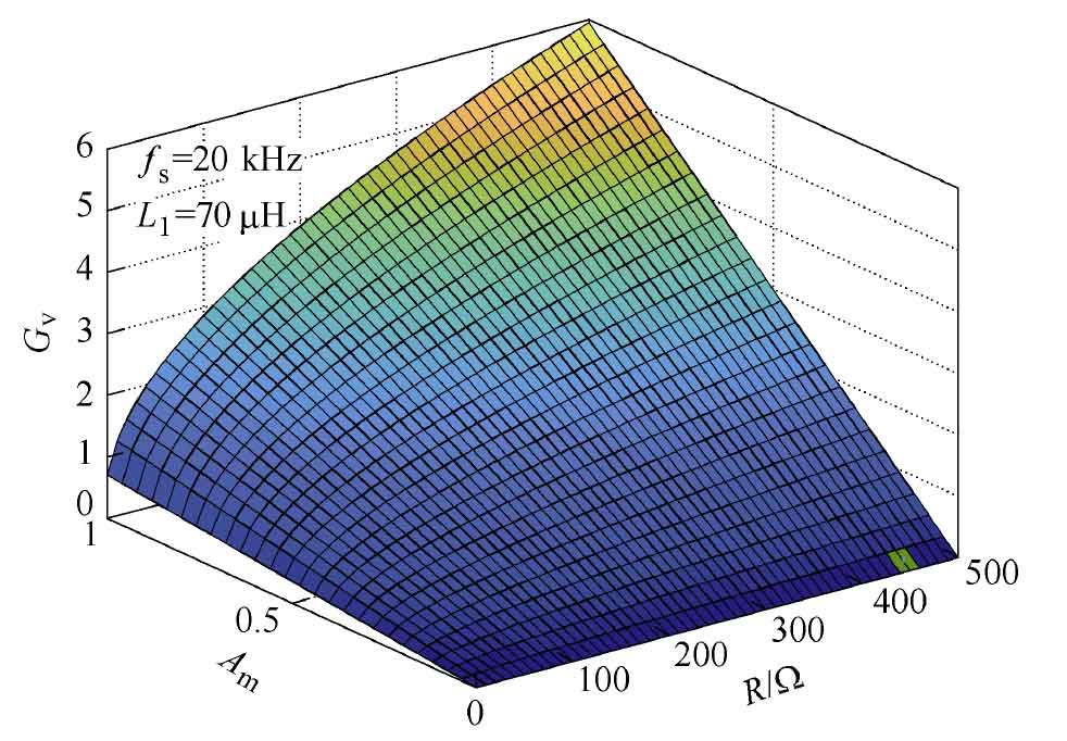
According to the formula, draw the output voltage gain curve of the proposed solar photovoltaic inverter in Figure 8, where fs and L1 are determined values. When the load is determined, the modulation coefficient Am is directly proportional to the voltage gain, so the low voltage grid connection on the photovoltaic side can be fully satisfied by adjusting Am. Considering safety margin, the voltage gain peak selection in this article should be below 6.
3.3 Comparative analysis
The output power quality of solar photovoltaic inverters is directly proportional to the number of levels, but in terms of the overall performance of the converter, this is not the case because a large number of levels require additional main power devices, which restricts the practical application of multi-level solar photovoltaic inverters. Therefore, the cost-effectiveness can to some extent measure the practicality of a solar photovoltaic inverter.
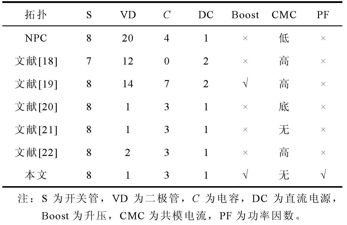
Taking single-phase five level as an example, Table 3 presents the comparison results between the recent solar photovoltaic inverters and the proposed solar photovoltaic inverters, including their functions and the number of semiconductor devices. The methods for achieving five levels in the above work can be divided into flying capacitor clamp type, diode clamp type, and H-bridge cascade type. However, diode clamp and H-bridge cascades require more power devices, increasing costs and losses. The flying capacitor type requires fewer components and has high practicality. Compared to capacitor clamped inverters, solar photovoltaic inverters have both reactive power feedback and high voltage gain characteristics, making them more compatible with photovoltaic cells that are more sensitive to environmental changes. This article does not have an advantage in the number of semiconductors, but requires a pre charging circuit to make the control unit complex, and the negative half cycle switching capacitor unit is not charged, resulting in severe output current distortion.
3.4 Loss Analysis
The total loss can be divided into switching loss and conduction loss. To simplify the analysis, the duty cycle of switches S4 to S8 is defined as D.
3.4.1 Switching losses
The switching loss includes the overlap loss PS of high-frequency voltage and current, as well as the charging loss PG of parasitic capacitors. Therefore, switch losses can be expressed as:
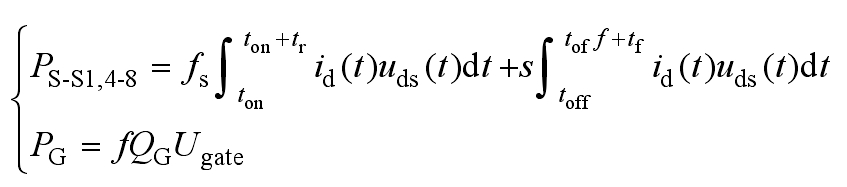
3.4.2 Conduction loss
The current in the power device is PWM, and its conduction time depends on the duty cycle. Therefore, the losses of high-frequency switches S1, S4 to S8, and power frequency switches S2 and S3 are:
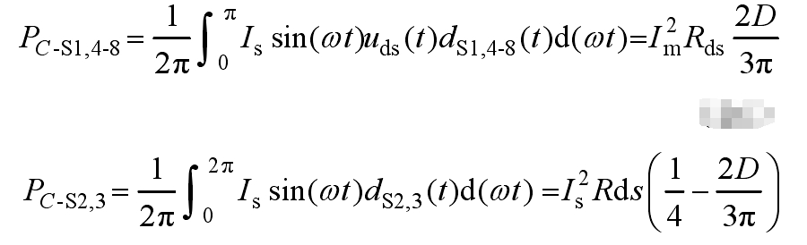
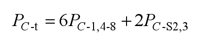
Furthermore, the total conduction loss can be obtained as:
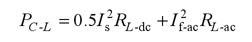
The conduction loss of inductance PC-L usually consists of two parts, namely the power frequency current conduction loss related to the DC resistance RL-dc and the high-frequency current ripple conduction loss related to the AC resistance RL-ac. Therefore, it can be concluded that:
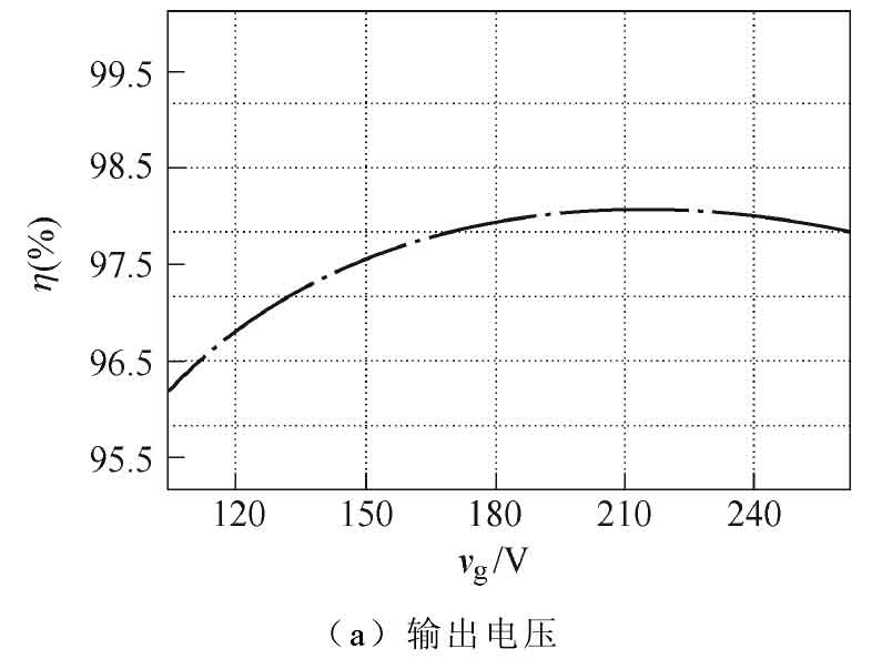
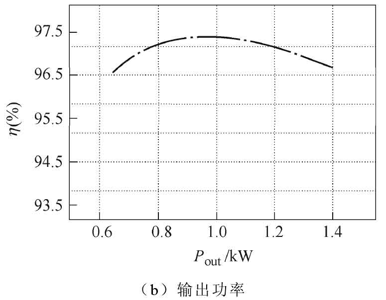
This article is based on the thermal model simulation of PSIM, and the efficiency curve is shown in Figure 9. It can be seen that the transmission efficiency is higher than 96.1% at different output voltage levels, and its efficiency is higher than 96.5% in the range of output power from 650 W to 1.3 kW.
4. Experimental verification
To verify the correctness and feasibility of the theoretical analysis process, a 1 kW experimental prototype was constructed in this paper. The specific circuit parameters are shown in Table 4. Figures 10 to 14 show the experimental waveforms of key electrical parameters.
| Parameters | Value (model) |
| Input voltage Vin/V | 60~100 |
| Output voltage vg | 120-240Vac |
| Switching frequency fs/kHz | 20 |
| Line frequency f/Hz | 50 |
| Capacitor C1/ μF | 250 (450 V) |
| Inductance L1/ μH | 70 |
| Filter inductance L2/mH | 2 |
| Switch tube | SVF740T TO − 220 |
| Diode | SE160 − 06A |
| Capacitor C2/μF | 250 (450 V) |
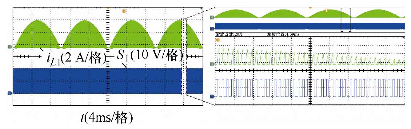
Figure 10 shows the current waveform of the DC side inductor L1 and the driving waveform of the switching transistor S1. From Figure 10, it can be seen that: ① the input current is symmetrical within the positive and negative cycles of the power frequency; ② The driving signal of switch S1 is SPWM signal, and both operate in intermittent working mode. The above process is consistent with theoretical analysis.
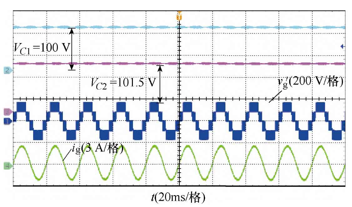
The proposed solar photovoltaic inverter topology can achieve self balancing of the switched capacitor network. Therefore, Figure 11 shows the test voltage waveforms of capacitors C1 and C2, as well as the output voltage gv ‘without LC filter. It can be seen that the voltage waveforms of the two capacitors overlap approximately; Simultaneously, the output side voltage is a standard five level stepped wave with good symmetry. The output waveform shows no distortion.
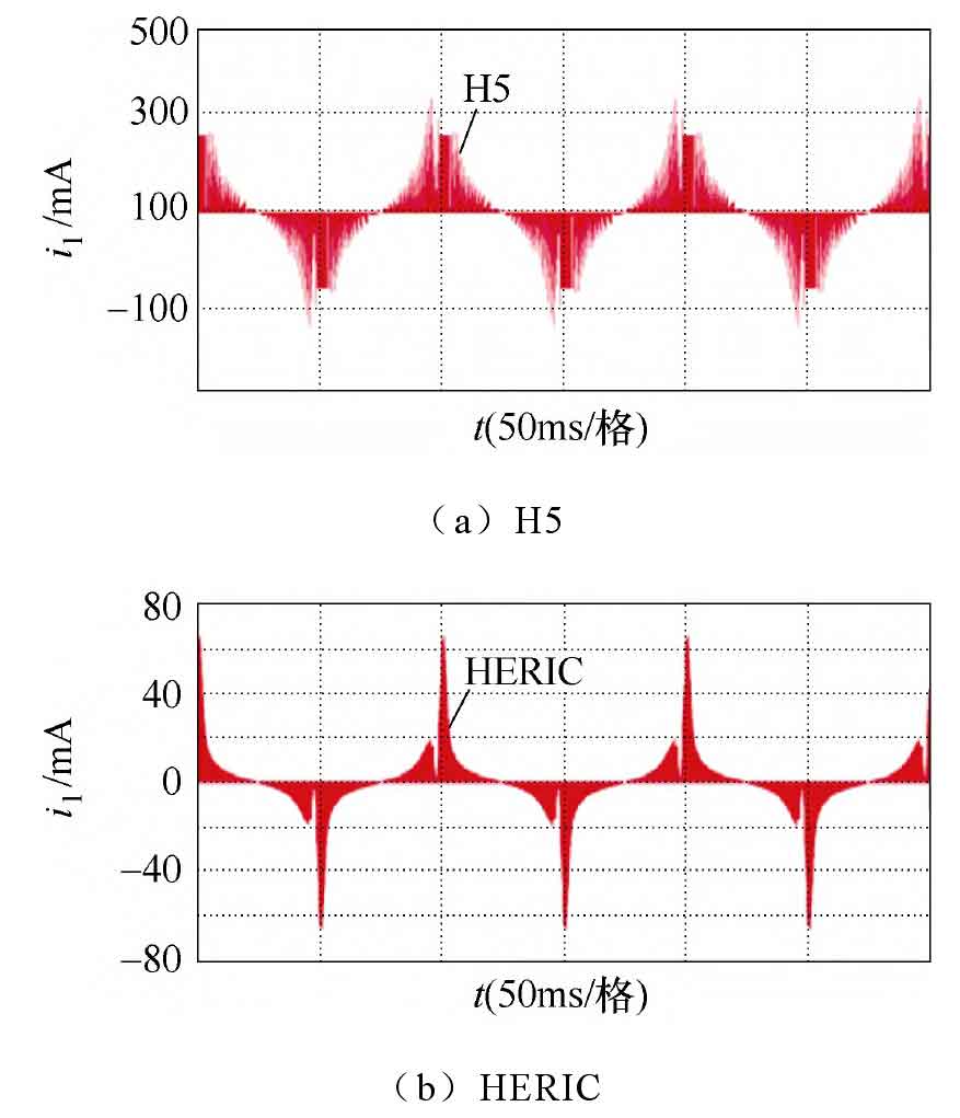
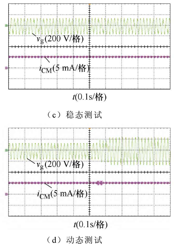
Based on the same component parameters, Figure 12 shows the measurement waveforms of H5, HERIC, and the proposed solar photovoltaic inverter topology leakage current. From Figures 12a and 12b, it can be seen that the maximum peak leakage currents of the H5 and HERIC topologies are 350 mA and 70 mA, respectively. The reason is that the topology itself is affected by the junction capacitance of the switching transistor, and the common mode voltage cannot be kept constant, resulting in the leakage current still existing, which intensifies with the increase of switching frequency. Figures 12c and 12d show the steady-state and dynamic leakage current test results of the proposed topology, respectively. It can be seen that the new topology clamps the common mode voltage to zero potential and keeps it constant, effectively avoiding the influence of leakage current.
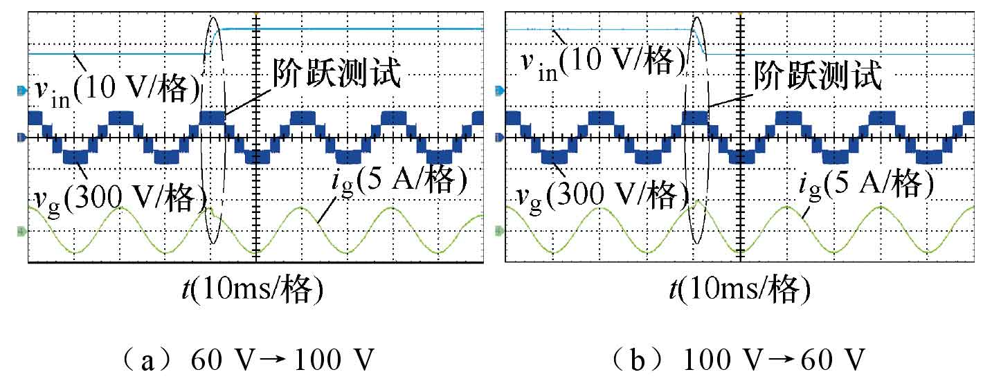
To verify the dynamic performance of the proposed solar photovoltaic inverter system, step tests of input voltage from 60 V to 100 V and from 100 V to 60 V are shown in Figure 13. It can be seen that the proposed solar photovoltaic inverter has good dynamic performance, and the total harmonic distortion (THD) of the output current of the inverter throughout the entire process measured by a harmonic analyzer (HIOKI3197) is less than 2.56%. In addition, the proposed solar photovoltaic inverter achieves the functions of boosting and inverting, and the sine degree of the output current waveform is good.
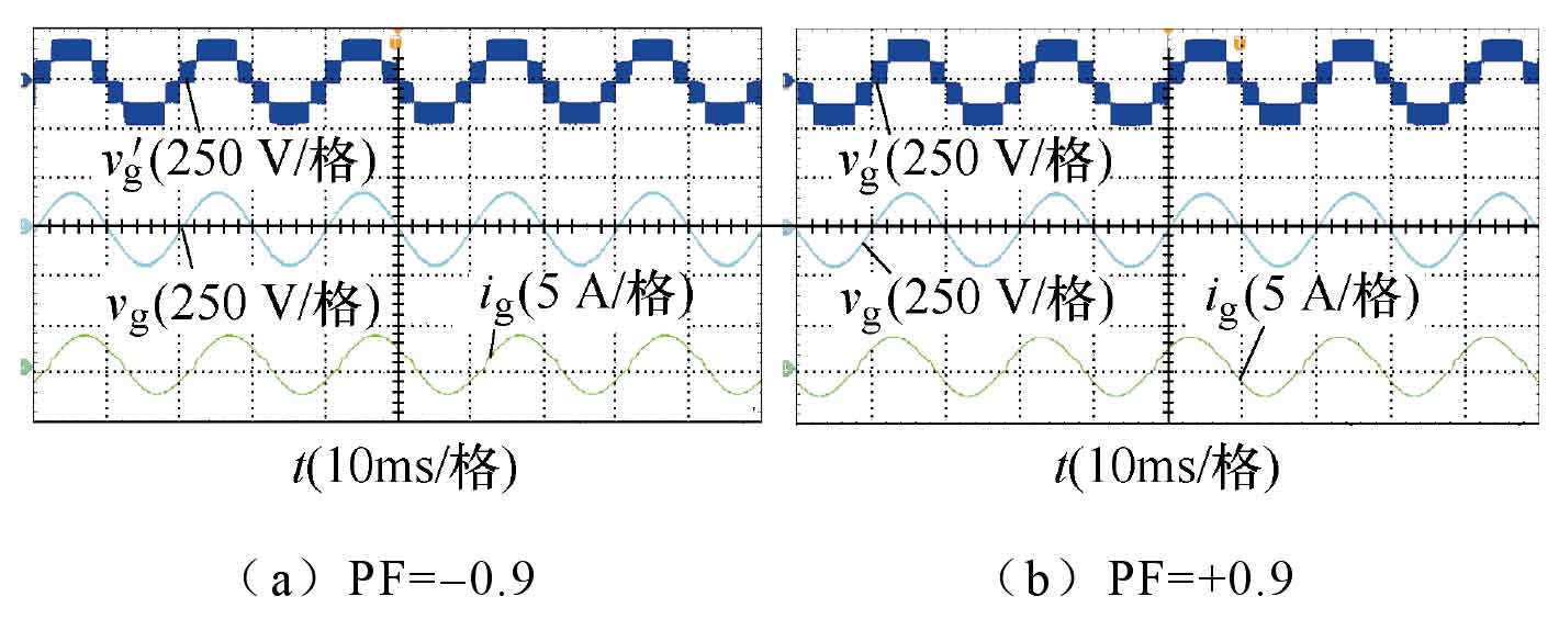
According to the VDE-ARN 4105 standard, grid connected solar photovoltaic inverters with a rated power below 3.68 kW should inject reactive power into the grid. Therefore, to verify the reactive power feeding capability of the proposed solar photovoltaic inverter, this paper adds a reactive power component to the current reference signal is ref. The test results in Figures 14a and 14b are obtained. At this time, the solar photovoltaic inverter operates stably at PF=-0.9 and PF=+0.9. It can be seen that the output current performs smoothly and without distortion, therefore this topology has the ability to provide reactive power support for the power grid. The proposed solar photovoltaic inverter topology has a wider range of applications.
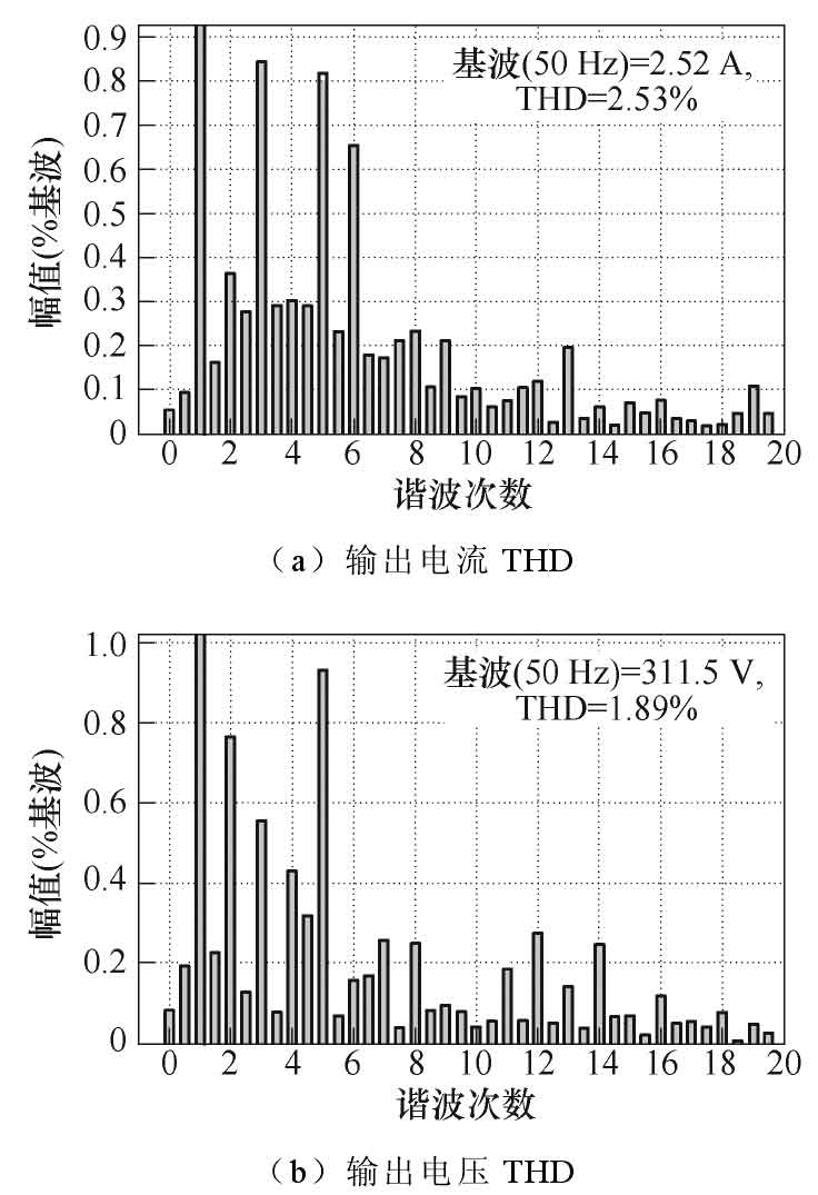
Figure 15 shows the test results of off grid output current and output voltage THD at fs=20 kHz, which are 1.89% and 2.52%, respectively. This harmonic meets the requirements of IEC 610003-2. This indicates that the photovoltaic array can achieve good integration with the proposed solar photovoltaic inverter.
5. Conclusion
A non isolated common ground multi-level solar photovoltaic inverter is proposed for low-voltage distributed photovoltaic grid connected systems. Through modal analysis, gain derivation, comparative analysis, and design considerations, the following conclusions have been drawn:
1) This topology structure has strong boosting function and capacitor voltage self balancing ability.
2) The common ground structure effectively suppresses the ground leakage current of photovoltaic cells without an isolation transformer, with a leakage inductance peak value below 5 mA.
3) This structure has reactive power support capability and can operate stably at PF=± 0.9.
4) Decoupling the output variable from the fluctuating capacitor voltage through a feedforward space vector modulation strategy to suppress output current harmonics. Its maximum current harmonic is only 2.52%.
Finally, a 1 kW experimental prototype was built. The results show that the proposed solar photovoltaic inverter has the above functions and good dynamic performance.